Issue 48, 2015

Direct patterning of sol–gel metal oxide semiconductor and dielectric films via selective surface wetting

Abstract

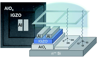
We report the simple, photolithography-free, direct patterning of both solution-processed metal oxide semiconductors and dielectrics via selective surface wetting. This technique was directly applied to fabrication of low-voltage all-solution metal oxide thin-film transistors with minimal channel and gate leakage currents.

Graphical abstract: Direct patterning of sol–gel metal oxide semiconductor and dielectric films via selective surface wetting

Supplementary files

Article information

Article type
Communication
Submitted
14 Mar 2015
Accepted
17 Apr 2015
First published
27 Apr 2015

RSC Adv., 2015,5, 38125-38129

Author version available

Direct patterning of sol–gel metal oxide semiconductor and dielectric films via selective surface wetting

S. Sung, S. Park, S. Cha, W. Lee, C. Kim and M. Yoon, RSC Adv., 2015, 5, 38125 DOI: 10.1039/C5RA04515K

To request permission to reproduce material from this article, please go to the Copyright Clearance Center request page.

If you are an author contributing to an RSC publication, you do not need to request permission provided correct acknowledgement is given.

If you are the author of this article, you do not need to request permission to reproduce figures and diagrams provided correct acknowledgement is given. If you want to reproduce the whole article in a third-party publication (excluding your thesis/dissertation for which permission is not required) please go to the Copyright Clearance Center request page.

Read more about how to correctly acknowledge RSC content.

Social activity

Spotlight

Advertisements