Heterodimers formed through a partial anionic exchange process: scanning tunneling spectroscopy to monitor bands across the junction vis-à-vis photoinduced charge separation†
Abstract
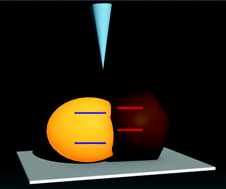
We report controlled formation of heterodimers and their charge separation properties. CdS|CdTe heterodimers were formed through an anionic exchange process of CdS nanostructures. With control over the duration of the anionic exchange process, bulk|dot, bulk|bulk, and then dot|bulk phases of the semiconductors could be observed to have formed. A mapping of density of states as derived from scanning tunneling spectroscopy (STS) brought out conduction and valence band-edges along the nanostructures and heterodimers. The CdS|CdTe heterodimers evidenced a type-II band-alignment between the semiconductors along with the formation of a depletion region at the interface. The width (of the depletion region) and the energy-offset at the interface depended on the size of the semiconductors. We report that the width that is instrumental for photoinduced charge separation in the heterodimers has a direct correlation with the performance of hybrid bulk-heterojunction solar cells based on the nanostructures in a polymer matrix.


 Please wait while we load your content...