Issue 26, 2015

Few layered MoS2 lithography with an AFM tip: description of the technique and nanospectroscopy investigations

Abstract

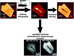
A novel technique to lithograph the MoS2 surface is described here. Mechanically exfoliated MoS2 flakes have been patterned with an atomic force microscope tip. After the patterning process, the lithographed areas have been removed by selective chemical etching. The electronic properties of the MoS2 flakes have been analyzed with spatially resolved photoelectron spectroscopy, with tunable incident photon energy, provided by a synchrotron light source. Tens of meV core level shifts can be recorded in relation to the flakes edges, coming from both the exfoliation and from the lithography.

Graphical abstract: Few layered MoS2 lithography with an AFM tip: description of the technique and nanospectroscopy investigations

Supplementary files

Article information

Article type
Paper
Submitted
12 Apr 2015
Accepted
26 May 2015
First published
29 May 2015

Nanoscale, 2015,7, 11453-11459

Few layered MoS2 lithography with an AFM tip: description of the technique and nanospectroscopy investigations

M. Donarelli, F. Perrozzi, F. Bisti, F. Paparella, V. Feyer, A. Ponzoni, M. Gonchigsuren and L. Ottaviano, Nanoscale, 2015, 7, 11453 DOI: 10.1039/C5NR02337H

To request permission to reproduce material from this article, please go to the Copyright Clearance Center request page.

If you are an author contributing to an RSC publication, you do not need to request permission provided correct acknowledgement is given.

If you are the author of this article, you do not need to request permission to reproduce figures and diagrams provided correct acknowledgement is given. If you want to reproduce the whole article in a third-party publication (excluding your thesis/dissertation for which permission is not required) please go to the Copyright Clearance Center request page.

Read more about how to correctly acknowledge RSC content.

Social activity

Spotlight

Advertisements