Single-digit-resolution nanopatterning with extreme ultraviolet light for the 2.5 nm technology node and beyond†
Abstract
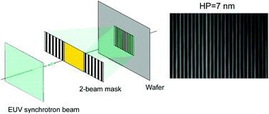
All nanofabrication methods come with an intrinsic resolution limit, set by their governing physical principles and instrumentation. In the case of extreme ultraviolet (EUV) lithography at 13.5 nm wavelength, this limit is set by light diffraction and is ≈3.5 nm. In the semiconductor industry, the feasibility of reaching this limit is not only a key factor for the current developments in lithography technologies, but also is an important factor in deciding whether photon-based lithography will be used for future high-volume manufacturing. Using EUV-interference lithography we show patterning with 7 nm resolution in making dense periodic line-space structures with 14 nm periodicity. Achieving such a cutting-edge resolution has been possible by integrating a high-quality synchrotron beam, precise nanofabrication of masks, very stable exposures instrumentation, and utilizing effective photoresists. We have carried out exposure on silicon- and hafnium-based photoresists and we demonstrated the extraordinary capability of the latter resist to be used as a hard mask for pattern transfer into Si. Our results confirm the capability of EUV lithography in the reproducible fabrication of dense patterns with single-digit resolution. Moreover, it shows the capability of interference lithography, using transmission gratings, in evaluating the resolution limits of photoresists.


 Please wait while we load your content...