In situ unravelling structural modulation across the charge-density-wave transition in vanadium disulfide†
Abstract
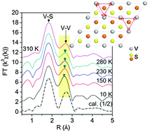
A deep understanding of the relationship between electronic and structure ordering across the charge-density-wave (CDW) transition is crucial for both fundamental study and technological applications. Herein, using in situ X-ray absorption fine structure (XAFS) spectroscopy coupled with high-resolution transmission electron microscopy (HRTEM), we have illustrated the atomic-level information on the local structural evolution across the CDW transition and its influence on the intrinsic electrical properties in VS2 system. The structure transformation, which is highlighted by the formation of vanadium trimers with derivation of V–V bond length (ΔR = 0.10 Å), was clearly observed across the CDW process. Moreover, the corresponding influence of lattice variation on the electronic behavior was clearly characterized by experimental results as well as theoretical analysis, which demonstrated that vanadium trimers drive the deformation of space charge density distribution into √3 × √3 periodicity, with the conductivity of a1g band reducing by half. These observations directly unveiled the close connection between lattice evolution and electronic property variation, paving a new avenue for understanding the intrinsic nature of electron-lattice interactions in the VS2 system and other isostructural transition metal dichalcogenides across the CDW transition process.


 Please wait while we load your content...