Patterning rubrene crystalline thin films for sub-micrometer channel length field-effect transistor arrays†
Abstract
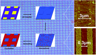
In this communication, a direct coupling of patterned growth of rubrene crystalline thin films with OFET fabrication is presented. The film was grown between pre-patterned Au electrodes covered with an organic monolayer, which directly allowed the fabrication of OFET devices with a sub-micrometer channel length. More importantly, close packed and porous film structures can be controlled by adjusting the space between the electrodes, resulting in a two orders of magnitude difference in carrier mobility. The technique is completely compatible with lithography methods thus may find potential applications in addressable and crosstalk suppressing OFET arrays.
 Please wait while we load your content...

