Plasma enhanced atomic layer deposition of Ga2O3 thin films
Abstract
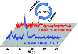
Amorphous Ga2O3 thin films have been grown on SiO2/Si substrates by atomic layer deposition (ALD) using tris (2,2,6,6-tetramethyl-3,5-heptanedionato) gallium(III) [Ga(TMHD)3] as a gallium source and O2 plasma as reactant. A constant growth rate of 0.1 Å per cycle was obtained in a broad temperature range starting from 100 to 400 °C. X-ray photoelectron spectroscopy (XPS) analysis revealed stoichiometric Ga2O3 thin films with no detectable carbon contamination. A double beam – double monochromator spectrophotometer was used to measure the transmittance of Ga2O3 thin films deposited on a quartz substrate and analysis of the adsorption edge yielded a band gap energy of 4.95 eV. The refractive index of the Ga2O3 films was determined from spectroscopic ellipsometry measurements and found to be 1.84 at a wavelength of 632.8 nm. Atomic force microscopic (AFM) analysis showed surface roughness values of 0.15 and 0.51 nm for films deposited at 200 and 400 °C, respectively. Finally, all the films could be crystallized into a monoclinic β-Ga2O3 crystal structure by a post deposition annealing in He as indicated by X-ray diffraction (XRD) measurements.


 Please wait while we load your content...