Ultraviolet emission of amorphous SiO2+x nanowires with connected bead-chain morphology†
Abstract
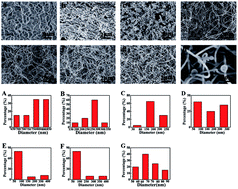
SiO2+x nanowires composed of multi-beads with novel chain morphology fabricated on an Au-coated silicon substrate were prepared via a chemical vapor deposition (CVD) technique. The morphology and microstructure of nanowires were characterized by scanning electron microscopy (SEM), transmission electron microscopy (TEM), selective area electron diffraction (SAED) and Fourier transform infrared spectroscopy (FTIR). The results showed that the morphology of SiO2+x could be well tuned by changing substrate temperature and deposition conditions. The growth process of SiO2+x nanowires was investigated by changing the substrate temperature from 400 °C to 1088 °C and the deposition time from 15 min to 60 min. Hence, a ‘dissolution–saturation–precipitation’ growth model suitable for the SiO2+x nanowires was proposed. Electron diffraction analysis showed that the nanowires had an amorphous phase structure. The SiO2+x nanowires emitted ultraviolet light with wavelengths of 308, 327 and 345 nm, respectively, which could be attributed to oxygen-rich composition of the nanowires.
 Please wait while we load your content...

