Anodic Cu2S and CuS nanorod and nanowall arrays: preparation, properties and application in CO2 photoreduction†
Abstract
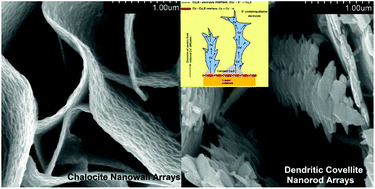
Copper sulfide semiconductors made from earth-abundant elements have an optical absorption edge at ca. 1.2 eV, nearly ideal for solar energy harvesting. We report the growth and formation mechanism of vertically oriented arrays of copper sulfide nanostructures formed by electrochemical anodization. Key parameters that affect the morphology and phase of the nanostructures are type and strength of electrolyte, anodization voltage and duration. Cu2S and CuS nanostructures were obtained on both copper foil and copper-coated flexible Kapton substrates, and depending on the anodization parameters, consisted of vertically oriented arrays of nanowalls, nanoleafs or rods with branched nanodendrites. The anodization parameters also controlled the phase and stoichiometry of the nanostructures. p-type conduction for Cu2S nanostructures and n-type conduction for CuS nanostructures were revealed by admittance spectroscopy and Mott Schottky analysis. We also observed a weak, but nevertheless promising and previously unnoticed, photocatalytic action in copper sulfide nanorod and platelet arrays for the sunlight-driven conversion of CO2 into CH4. Under irradiation by AM 1.5G simulated sunlight at room temperature, a CH4 production rate as high as 38 μmol m−2 h−1 was obtained using the copper sulfide nanostructure arrays as stand-alone photocatalysts for CO2 photoreduction.


 Please wait while we load your content...