Scalable graphene synthesised by plasma-assisted selective reaction on silicon carbide for device applications†
Abstract
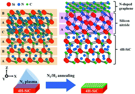
Graphene, a two-dimensional material with honeycomb arrays of carbon atoms, has shown outstanding physical properties that make it a promising candidate material for a variety of electronic applications. To date, several issues related to the material synthesis and device fabrication need to be overcome. Despite the fact that large-area graphene films synthesised by chemical vapour deposition (CVD) can be grown with relatively few defects, the required transfer process creates wrinkles and polymer residues that greatly reduce its performance in device applications. Graphene synthesised on silicon carbide (SiC) has shown outstanding mobility and has been successfully used to develop ultra-high frequency transistors; however, this fabrication method is limited due to the use of costly ultra-high vacuum (UHV) equipment that can reach temperatures over 1500 °C. Here, we show a simple and novel approach to synthesise graphene on SiC substrates that greatly reduces the temperature and vacuum requirements and allows the use of equipment commonly used in the semiconductor processing industry. In this work, we used plasma treatment followed by annealing in order to obtain large-scale graphene films from bulk SiC. After exposure to N2 plasma, the annealing process promotes the reaction of nitrogen ions with Si and the simultaneous condensation of C on the surface of SiC. Eventually, a uniform, large-scale, n-type graphene film with remarkable transport behaviour on the SiC wafer is achieved. Furthermore, graphene field effect transistors (FETs) with high carrier mobilities on SiC were also demonstrated in this study.


 Please wait while we load your content...