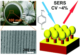
300 mm Wafer-level, ultra-dense arrays of Au-capped nanopillars with sub-10 nm gaps as reliable SERS substrates†
Abstract
The 193 nm deep UV immersion lithography is leveraged to fabricate highly dense and uniform arrays of Au-capped Si nanopillars on a 300 mm wafer level, and the substrates are applied in surface enhanced Raman spectroscopy for reliable molecule detection. Due to the sub-10 nm gap sizes and ultra-high array density with the lattice constant less than 100 nm, our nanopillar based substrates outperform the current commercial products in terms of the signal intensity, reproducibility and fabrication scale.
 Please wait while we load your content...

