Three-dimensional hierarchical Te–Si nanostructures†
Abstract
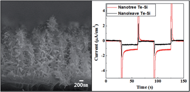
Three-dimensional hybrid nanostructures (i.e., Te “nanobranches” on a Si “nanotrunk” or Te “nanoleaves” on a Si “nanotrunk”) were synthesized by combining the gold-assisted chemical etching of Si to form Si “nanotrunks” and the galvanic displacement of Si to form Te “nanobranches” or “nanoleaves.” By adjusting the composition of the electrolyte used for the galvanic displacement reaction, the shape of the Te nanostructures could be changed from nanoleaves to nanobranches. The Si nanotrunks with Te nanobranches showed stronger luminescent emission in the visible region, with their Raman spectrum having a higher wave number, owing to their grain size being larger. This suggested that the optical and photoelectrochemical properties of Te–Si hybrid nanostructures depend on their shape and size. Using this approach, it should be possible to fabricate various hierarchical nanostructures for use in photoelectronic and photoelectrochemical devices.


 Please wait while we load your content...