Large-scale, solution-phase growth of semiconductor nanocrystals into ultralong one-dimensional arrays and study of their electrical properties†
Abstract
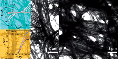
One-dimensional (1D) assemblies of semiconductor nanocrystals (NCs) represent an important kind of 1D nanomaterial system due to their potential for exploring novel and enhanced electronic and photonic performances of devices. Herein, we present mass fabrication of a series of 1D arrays of CdSe and PbSe NCs on a large length scale with ultralong, aligned Se nanowires (NWs) as both the reactant and structure-directing template. The 1D self-assembly patterns are the anchored growth of CdSe quantum dots (QDs) on the surface of Se NWs (i.e., 1D Se NWs/CdSe QDs core–shell heterostructure) and 1D aggregates of unsupported PbSe NCs formed by substantially increased collective particle–particle interactions. The size of CdSe QDs and shape of PbSe NCs in the 1D arrays can be effectively controlled by varying the synthetic conditions. Room temperature electrical measurements on the 1D Se/CdSe heterostructure field effect transistors (FETs) exhibit a pronounced improvement in the on/off ratio, device carrier mobility, and transconductance compared to the Se NW FETs fabricated in parallel. Furthermore, upon visible light excitation, the photocurrent from the Se/CdSe heterostructure FETs responses sharply (small time constant) and increases linearly with increasing the light intensity, indicating excellent photoconductive properties.
 Please wait while we load your content...

