Electrochemical properties of CVD grown pristine graphene: monolayer- vs. quasi-graphene†
Abstract
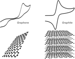
We report the electrochemical properties of pristine monolayer, double layer and few-layer (termed quasi-) graphene grown via CVD and transferred using PMMA onto an insulating substrate (silicon dioxide wafers). Characterisation has been performed by Raman spectroscopy, optical spectroscopy, Atomic Force Microscopy and X-ray Photoelectron Spectroscopy, revealing ‘true’ pristine single-layer graphene (O/C of 0.05) at the former and pristine quasi-graphene at the latter (O/C of 0.07); the term “quasi-graphene” is coined due to the surface comprising on average 4-graphene-layers. The graphene electrodes are electrochemically characterised using both inner-sphere and outer-sphere redox probes with electrochemical performances of the graphene electrodes compared to other available graphitic electrodes, namely that of basal- and edge- plane pyrolytic graphite electrodes constructed from Highly Ordered Pyrolytic Graphite (HOPG), with information on heterogeneous rate constants (ko) obtained. The electrochemical rate constants are predominantly influenced by the electronic properties of the graphene surfaces. Monolayer graphene is found to exhibit slow heterogeneous electron transfer (HET) kinetics towards the redox probes studied, with HET rates ca. 2 and 8 times faster at quasi-graphene and HOPG respectively, relative to that of the monolayer graphene electrode. Critically contrasting the performance of monolayer graphene to quasi-graphene and HOPG electrodes reveals that increasing the number of graphene layers results in improved electrochemical properties, where in terms of the electrochemical reversibility of the probes studied: monolayer-graphene < quasi-graphene < HOPG, as governed by the respective HET electrochemical rate constants. Given that edge plane sites are the predominant origin of fast electron transfer kinetics at graphitic materials, the slow HET rates at pristine single-layer graphene electrodes are likely due to graphene’s fundamental geometry, which comprises a small edge plane and large basal plane contribution. In the case of quasi-graphene and HOPG, they possess increasing global coverage of electrochemically reactive edge plane sites (respectively) and thus exhibit superior electrochemical performances over that of monolayer graphene. Last, the case of a double-layer graphene electrode is considered, which as a result of its fabrication possesses a large global coverage of edge plane like- sites/defects. In agreement with the former conclusions, the double-layered defect-graphene electrode is found to exhibit fast/favourable electrochemical properties, which is attributed to its large edge plane content (i.e. defect abundant graphene) and thus is further evidence that the electrochemical response is dependent on the density of edge plane sites at graphene based electrodes (influenced by the coverage of graphene-defects and the number of graphene layers).


 Please wait while we load your content...