Scanning tunnelling microscopy of epitaxial nanostructures
Abstract
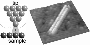
Epitaxial nanostructures have generated a great deal of interest because of the applications in catalysis, photonics and nanoelectronics. To study the structure and electronic properties at the nanoscale, scanning tunnelling microscopy (STM) has proven a very effective technique due to its extraordinarily high spatial resolution. Growth modes of epitaxial nanostructures depend predominantly on the surface free energy of the deposited material, and that of the substrate onto which it is deposited, leading to layer-by-layer or island growth modes. The strain due to lattice mismatch plays an important role in the formation of semiconductor quantum dot islands via strain-induced transitions in the morphology of epitaxial nanoislands. Examples of the different growth modes observed with STM are presented in this review within a general framework that uses the surface and strain energies to understand the effects that govern nanostructure shapes. Some self-assembled oxide and metal nanostructures, as well as molecular networks, are also discussed.

- This article is part of the themed collection: Nucleation and crystallisation

 Please wait while we load your content...