Issue 32, 2014

Significant quality improvement of GaN on Si(111) upon formation of an AlN defective layer

Abstract

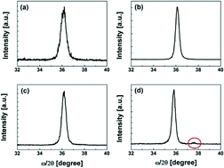
The stress state and crystal quality of a metal–organic chemical vapor deposition (MOCVD)-grown GaN film on a Si(111) substrate with different AlN buffer layer thicknesses were investigated. The properties of the AlN layers with varying thicknesses were studied. The three-dimensional growth mode with a rough surface of AlN on Si was observed. A defective layer with mixed orientations of AlN grains formed at the AlN/GaN interface. The AlN buffer layer with the defective layer accommodated most of the lattice mismatch between the GaN film and the Si substrate. The significance of the defective layer was proved by the obtainment of a 1 μm thick nearly crack-free GaN film with high crystal quality.

Graphical abstract: Significant quality improvement of GaN on Si(111) upon formation of an AlN defective layer

Article information

Article type
Paper
Submitted
08 Jun 2014
Accepted
16 Jun 2014
First published
16 Jun 2014

CrystEngComm, 2014,16, 7525-7528

Significant quality improvement of GaN on Si(111) upon formation of an AlN defective layer

Y. Feng, H. Wei, S. Yang, H. Zhang, S. Kong, G. Zhao and X. Liu, CrystEngComm, 2014, 16, 7525 DOI: 10.1039/C4CE01164C

To request permission to reproduce material from this article, please go to the Copyright Clearance Center request page.

If you are an author contributing to an RSC publication, you do not need to request permission provided correct acknowledgement is given.

If you are the author of this article, you do not need to request permission to reproduce figures and diagrams provided correct acknowledgement is given. If you want to reproduce the whole article in a third-party publication (excluding your thesis/dissertation for which permission is not required) please go to the Copyright Clearance Center request page.

Read more about how to correctly acknowledge RSC content.

Social activity

Spotlight

Advertisements