Issue 3, 2013

Three-dimensional etching of silicon for the fabrication of low-dimensional and suspended devices

Abstract

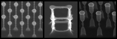
In order to expand the use of nanoscaled silicon structures we present a new etching method that allows us to shape silicon with sub-10 nm precision. This top-down, CMOS compatible etching scheme allows us to fabricate silicon devices with quantum behavior without relying on difficult lateral lithography. We utilize this novel etching process to create quantum dots, quantum wires, vertical transistors and ultra-high-aspect ratio structures. We believe that this etching technique will have broad and significant impacts and applications in nano-photonics, bio-sensing, and nano-electronics.

Graphical abstract: Three-dimensional etching of silicon for the fabrication of low-dimensional and suspended devices

Supplementary files

Article information

Article type
Communication
Submitted
28 Sep 2012
Accepted
11 Dec 2012
First published
13 Dec 2012

Nanoscale, 2013,5, 927-931

Three-dimensional etching of silicon for the fabrication of low-dimensional and suspended devices

S. S. Walavalkar, A. P. Homyk, M. D. Henry and A. Scherer, Nanoscale, 2013, 5, 927 DOI: 10.1039/C2NR32981F

To request permission to reproduce material from this article, please go to the Copyright Clearance Center request page.

If you are an author contributing to an RSC publication, you do not need to request permission provided correct acknowledgement is given.

If you are the author of this article, you do not need to request permission to reproduce figures and diagrams provided correct acknowledgement is given. If you want to reproduce the whole article in a third-party publication (excluding your thesis/dissertation for which permission is not required) please go to the Copyright Clearance Center request page.

Read more about how to correctly acknowledge RSC content.

Social activity

Spotlight

Advertisements