Issue 19, 2013

Cell patterningvia diffraction-induced optoelectronic dielectrophoresis force on an organic photoconductive chip

Abstract

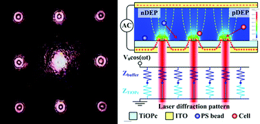
A laser diffraction-induced dielectrophoresis (DEP) phenomenon for the patterning and manipulation of individual HepG2 cells and polystyrene beads via positive/negative DEP forces is reported in this paper. The optoelectronic substrate was fabricated using an organic photoconductive material, TiOPc, via a spin-coating process on an indium tin oxide glass surface. A piece of square aperture array grid grating was utilized to transform the collimating He–Ne laser beam into the multi-spot diffraction pattern which forms the virtual electrodes as the TiOPc-coating surface was illuminated by the multi-spot diffraction light pattern. HepG2 cells were trapped at the spot centers and polystyrene beads were trapped within the dim region of the illuminated image. The simulation results of light-induced electric field and a Fresnel diffraction image illustrated the distribution of trapped microparticles. The HepG2 morphology change, adhesion, and growth during a 5-day culture period demonstrated the cell viability through our manipulation. The power density inducing DEP phenomena, the characteristics of the thin TiOPc coating layer, the operating ac voltage/frequency, the sandwiched medium, the temperature rise due to the ac electric fields and the illuminating patterns are discussed in this paper. This concept of utilizing laser diffraction images to generate virtual electrodes on our TiOPc-based optoelectronic DEP chip extends the applications of optoelectronic dielectrophoretic manipulation.

Graphical abstract: Cell patterning via diffraction-induced optoelectronic dielectrophoresis force on an organic photoconductive chip

Supplementary files

Article information

Article type
Paper
Submitted
18 Mar 2013
Accepted
06 Jul 2013
First published
08 Jul 2013

Lab Chip, 2013,13, 3893-3902

Cell patterning via diffraction-induced optoelectronic dielectrophoresis force on an organic photoconductive chip

S. Yang, S. Tseng, H. Chen, L. Hsu and C. Liu, Lab Chip, 2013, 13, 3893 DOI: 10.1039/C3LC50351H

To request permission to reproduce material from this article, please go to the Copyright Clearance Center request page.

If you are an author contributing to an RSC publication, you do not need to request permission provided correct acknowledgement is given.

If you are the author of this article, you do not need to request permission to reproduce figures and diagrams provided correct acknowledgement is given. If you want to reproduce the whole article in a third-party publication (excluding your thesis/dissertation for which permission is not required) please go to the Copyright Clearance Center request page.

Read more about how to correctly acknowledge RSC content.

Social activity

Spotlight

Advertisements