Issue 39, 2012

ZnO layers for opto-electronic applications from solution-based and low-temperature processing of an organometallic precursor

Abstract

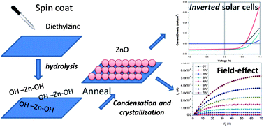
As printed and flexible plastic electronic gadgets become increasingly viable today, there is a need to develop materials that suit the fabrication processes involved. Two desirable requirements are solution-processable active materials or precursors and low-temperature processability. In this article, we describe a straightforward method of depositing ZnO films by simple spin coating of an organometallic diethylzinc precursor solution and annealing the resulting film at low temperatures (≤200 °C) without involving any synthetic steps. By controlling the humidity in which annealing is conducted, we are able to adjust the intrinsic doping level and carrier concentration in diethylzinc-derived ZnO. Doped or conducting transport layers are greatly preferable to undoped layers as they enable low-resistance contacts and minimize the potential drops. This ability to controllably realize doped ZnO is a key feature of the fabrication process that we describe in this article. We employ field-effect measurements as a diagnostic tool to measure doping levels and mobilities in ZnO and demonstrate that doped ZnO with high charge carrier concentration is ideal for solar cell applications. Respectable power conversion efficiencies (up to 4.5%) are achieved in inverted solar cells that incorporate diethylzinc-derived ZnO films as the electron transport layer and organic blends as the active material. Extensions of this approach to grow ternary and quaternary films with organometallic precursor chemicals will enable solution based growth of a number of semiconductor films as well as a method to dope them.

Graphical abstract: ZnO layers for opto-electronic applications from solution-based and low-temperature processing of an organometallic precursor

Article information

Article type
Paper
Submitted
16 Jul 2012
Accepted
16 Aug 2012
First published
16 Aug 2012

J. Mater. Chem., 2012,22, 20896-20901

ZnO layers for opto-electronic applications from solution-based and low-temperature processing of an organometallic precursor

T. R. Bao Foong, S. P. Singh, P. Sonar, Z. Ooi, K. L. Chan and A. Dodabalapur, J. Mater. Chem., 2012, 22, 20896 DOI: 10.1039/C2JM34656G

To request permission to reproduce material from this article, please go to the Copyright Clearance Center request page.

If you are an author contributing to an RSC publication, you do not need to request permission provided correct acknowledgement is given.

If you are the author of this article, you do not need to request permission to reproduce figures and diagrams provided correct acknowledgement is given. If you want to reproduce the whole article in a third-party publication (excluding your thesis/dissertation for which permission is not required) please go to the Copyright Clearance Center request page.

Read more about how to correctly acknowledge RSC content.

Spotlight

Advertisements