Issue 2, 2011

Resistive switching memory: observations with scanning probe microscopy

Abstract

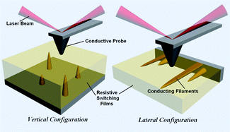
Recent advances in information technology require higher-speed and higher-density memory devices. In the past decade, resistance switching memory has emerged as a powerful alternative to existing charge-storage-based, non-volatile devices. Despite the extensive research, much of the underlying switching/conduction mechanism is still unknown and controversial. The versatile capability of scanning probe microscopy (SPM) has extended the understanding of resistive switching significantly. This review summarizes the recent advances in understanding on the mechanism of resistive switching effects with particular focus on SPM based observations. In addition, the tip–sample interfacial effects and resulting possible artefacts during scanning probe measurements are discussed.

Graphical abstract: Resistive switching memory: observations with scanning probe microscopy

Article information

Article type
Review Article
Submitted
11 Aug 2010
Accepted
09 Oct 2010
First published
25 Nov 2010

Nanoscale, 2011,3, 490-502

Resistive switching memory: observations with scanning probe microscopy

M. H. Lee and C. S. Hwang, Nanoscale, 2011, 3, 490 DOI: 10.1039/C0NR00580K

To request permission to reproduce material from this article, please go to the Copyright Clearance Center request page.

If you are an author contributing to an RSC publication, you do not need to request permission provided correct acknowledgement is given.

If you are the author of this article, you do not need to request permission to reproduce figures and diagrams provided correct acknowledgement is given. If you want to reproduce the whole article in a third-party publication (excluding your thesis/dissertation for which permission is not required) please go to the Copyright Clearance Center request page.

Read more about how to correctly acknowledge RSC content.

Social activity

Spotlight

Advertisements