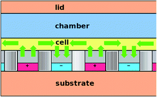
Interdigital electrode structures (IDES) play a major role in many technical and analytical applications. In particular, they are a key technology in modern lab-on-a-chip (LOC) devices. As high sensitivity is a key component of any (bio)analytical method, the presented work is aimed at designing a novel dielectric sensing system, which exhibits maximum sensor sensitivity using passivated dielectric microsensors. Although the implementation of high-εr dielectric passivation materials such as tantalum oxide or titanium oxide showed increased sensor sensitivity by a factor of 5, simulations revealed that sensor sensitivity is ultimately determined by the dielectric properties of the analyte. Ideally, dielectric properties of the passivation material need to be adjusted to the dielectric properties of the material under investigation and any deviations (e.g. higher or lower dielectric constants) will result in significant loss of sensitivity. To address these shortcomings we have developed a novel dielectric sensing concept based on a dual-material passivation geometry. The novel design consists of electric flux barriers that are layered between the finger electrodes, as well as electric flux guides which are located above the electrode structures that direct the entire generated electric flux to the object under investigation. Our 3D numerical results clearly show that the novel design offers two main advantages: firstly, the measurement sensitivity is further increased by more than a factor of two in comparison to a homogeneous passivation material sensing strategy. Secondly, maximum sensitivity for a given set of finger geometries can be achieved using a single sensor design regardless of the frequency-dependent dielectric properties of the measured objects. Hence, the novel approach is capable of reducing design and manufacturing costs of lab-on-a-chip devices.
You have access to this article
 Please wait while we load your content...
Something went wrong. Try again?
Please wait while we load your content...
Something went wrong. Try again?