Thinning vertical graphenes, tuning electrical response: from semiconducting to metallic†
Abstract
A simple, uniquely plasma-enabled and environment-friendly process to reduce the thickness of vertically standing
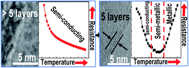
A simple, uniquely plasma-enabled and environment-friendly process to reduce the thickness of vertically standing
D. H. Seo, S. Kumar and K. (. Ostrikov, J. Mater. Chem., 2011, 21, 16339 DOI: 10.1039/C1JM13835A
To request permission to reproduce material from this article, please go to the Copyright Clearance Center request page.
If you are an author contributing to an RSC publication, you do not need to request permission provided correct acknowledgement is given.
If you are the author of this article, you do not need to request permission to reproduce figures and diagrams provided correct acknowledgement is given. If you want to reproduce the whole article in a third-party publication (excluding your thesis/dissertation for which permission is not required) please go to the Copyright Clearance Center request page.
Read more about how to correctly acknowledge RSC content.
 Please wait while we load your content...