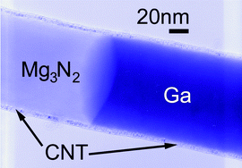
Semiconducting nanowire heterostructures with well-controlled dimensions, compositions and crystallinities represent a new class of intriguing systems for the investigation of structure–property relationships and related applications. This feature article reviews our recent research progress in the design and utilization of templating methods for preparing axial (including nanotube shielded metal–semiconductor nanowire heterojunctions), radial (including side-to-side biaxial and sandwiched triaxial semiconductor nanowire heterostructures), and branched semiconducting (including self-assembly of semiconductor nanowires into hierarchical heterostructures) nanowire heterostructures with desired atomic structures, interfaces, morphologies, properties, and potential applications to meet the growing demands and specific requirements of new technologies.
You have access to this article
 Please wait while we load your content...
Something went wrong. Try again?


 Please wait while we load your content...