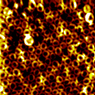
A modified nanosphere lithographic method for producing arrays of silanized structures at silicon surfaces is described. Polystyrene (PS) particles (600 nm or 1000 nm in diameter) were self-assembled onto a silicon substrate to form a hexagonal close-packed pattern. The resultant patterned surface was then exposed to a solution of 3-aminopropyltriethoxysilane (APTS), which deposited gradually in the interstitial voids of the PS particle array. When such a surface was sonicated in toluene to dislodge the PS particles, a mesoporous network containing truncated PS nanorings/shells was produced. Gold nanoparticles or DNA-capped gold nanoparticles, which are both negatively charged, can be electrostatically attached onto the PS/APTS nanoring array. Atomic force microscopy (AFM) was used to image the surface pattern and structure after each step of the procedure, while X-ray photoelectron spectra (XPS) and UV-visible spectrometry were used to determine the composition of the surface patterns. The mechanisms for forming the PS/APTS nanostructures are discussed. These structures could potentially be used as biosensors, heterogeneous catalysts, and functionalized nano-devices.

You have access to this article
 Please wait while we load your content...
Something went wrong. Try again?


 Please wait while we load your content...