
 Open Access Article
 This Open Access Article is licensed under a
 Creative Commons Attribution 3.0 Unported Licence
Morphology – composition correlations in carbon nanotubes synthesised with nitrogen and phosphorus containing precursors†
Rebecca J.
Nicholls
*a,
Zabeada
Aslam‡
a,
Michael C.
Sarahan§
b,
Ana M.
Sanchez
c,
Frank
Dillon
a,
Antal A.
Koós¶
a,
Peter D.
Nellist
ab and
Nicole
Grobert
a
aDepartment of Materials, University of Oxford, Oxford OX1 3PH, UK. E-mail: rebecca.nicholls@materials.ox.ac.uk
bSuperSTEM Laboratory, STFC Daresbury, Warrington WA4 4AD, UK
cDepartment of Physics, University of Warwick, Coventry CV4 7AL, UK
First published on 21st November 2014
Abstract
We have correlated the elemental composition with the structure of multi-wall carbon nanotubes synthesised with nitrogen and phosphorus containing precursors and identified two chemically distinct dominant morphologies. The first type are cone-structured tubes and the second are nanotubes with fewer walls which can accommodate N2 gas along their inner channel and contain up to ten times more nitrogen than the cone-structured nanotubes. Phosphorus was present in the catalyst particles but was not detected within the walls of either type of nanotube. Elemental analysis combined with in situ electrical measurements has allowed us to monitor the evolution of the doped nanotubes when current is passed. The N2 gas becomes bonded immediately when current flows and the gas-containing nanotubes restructure more easily than the cone-structured ones. Since the inclusion of heteroatoms in multi-wall carbon nanotubes is generally inhomogeneous, understanding the distribution of elements across the sample is an important step towards the optimization of devices including gas sensors and components in electrical applications.
Introduction
Carbon nanotubes have potential applications in domestic and industrial gas sensors1 and a nanotube-based gas sensor for monitoring landfill sites has already been developed.2 The advantages of using carbon nanotubes as gas sensors come from the small and light sensing element1 and the fact that they can detect small concentrations of gaseous species.3 Modifying the surface properties of the nanotube by including heteroatoms can alter the sensitivity of the tubes to different gaseous species by providing sites for the gas molecules to bind to. Multi-wall nanotubes synthesised from precursors containing phosphorus and nitrogen (P,N-MWCNTs) are a promising candidate for gas sensors. They have been predicted to have good molecular sensing properties4 and their selectivity has already been shown experimentally.5In general, heteroatoms are not incorporated homogenously throughout a carbon nanotube sample and this leads to a variety of nanostructures with different properties contained within the material.4,6,7 Although previous work on P,N-MWCNTs has reported a variation in the heteroatom concentration,8 the link between the local chemistry and large scale properties has not been made as either bulk measurements or measurements from a very small number of nanotubes have been carried out. Understanding this link and the variations in heteroatom concentration is an important step towards optimizing devices based on P,N-MWCNTs.
In this work, electron energy loss spectroscopy (EELS) and imaging within a (scanning) transmission electron microscope ((S)TEM) are used to investigate the link between the morphology and chemical composition of nanostructures within P,N-MWCNT samples produced by aerosol assisted chemical vapour deposition (CVD). This work identifies two types of P,N-MWCNT which have different morphologies and heteroatom concentrations. The electrical properties are also important for the design of devices, including sensors, and so in situ TEM experiments are performed to look at the effect of electrical currents on the different nanotubes morphologies. The information obtained about the variation of heteroatom concentration can be fed back into the synthesis process to see if it is possible to produce samples with more uniform heteroatom concentrations and, therefore, more uniform properties.
Experimental section
P,N-MWCNTs were synthesized using an aerosol assisted CVD system as described in ref. 5. Briefly, 2.5 wt% triphenylphosphine and 7.5 wt% ferrocene in benzylamine were decomposed at 780 °C in Ar. (S)TEM imaging and EELS measurements on the sample were carried out on a JEOL 3000F (operated at 300 kV) and a JEOL ARM200F (operated at 80 kV). SMART line-scans9 were performed using an aberration corrected Nion UltraSTEM equipped with a Gatan Enfina spectrometer and operated at 60 keV. In situ current measurements were carried out using a Nanofactory™ TEM-STM holder in both a JEOL 2010 (operated at 200 kV) and JEOL 3000F. For the conductivity measurements, the P,N-MWCNTs were mounted on a gold support wire and contacted with a second gold wire.Results and discussion
A TEM overview of the P,N-MWCNT sample (Fig. 1a) shows clean nanotubes with a variety of diameters and structures, as well as catalyst particles trapped inside some of the nanotubes. Two dominant nanotube morphologies are observed within the P,N-MWCNT sample and most, but not all, of the nanotubes can be identified as one or the other (see ESI†). The first type of nanotube, referred to as Type A, contains cone structures and examples of Type A nanotubes are shown in Fig. 1b and c. The nanotube in 1b has more walls that in 1c, and Type A nanotubes with more walls tend to have disordered outer layers. The second type of nanotube (Type B) has few walls (the inner diameter is greater than the thickness of the wall) and examples of this morphology are shown in Fig. 1d and e. The internal channel structure in Type B nanotubes varies from nanotubes which have frequent bridging (Fig. 1e) to those which show almost none (Fig. 1d). Often Type B nanotubes without much internal structure will have amorphous material on the inner walls. As well as a variation in morphology from one nanotube to another, it is also possible for the structure of an individual nanotube to change, as marked by an arrow in Fig. 1a where a nanotube changes from Type A (right-hand side) to Type B (left-hand side). (A larger image of the same area is shown in Fig. S2 of the ESI.†) | ||
| Fig. 1 (a) An overview of the P,N-MWCNT sample showing the variation in nanotube structures. (b and c) Examples of nanotubes with a Type A morphology. (d and e) Examples of nanotubes with a Type B morphology. An example of amorphous material on the inner-wall of the nanotube is marked by an arrow in (d) (a larger version of the same nanotube is shown in the ESI,† Fig. S1). | ||
To examine the link between nanotube morphology and heteroatom concentration, EELS spectra were taken from individual nanotubes with morphologies which could be easily classified as either Type A or Type B. EELS spectra contain core-loss edges which result from the beam losing energy by exciting core-electrons within the sample. As the energy required to excite a core-electron depends on the element to which it belongs, each element appears as a separate edge within the spectrum. The area under an edge is proportional to the number of atoms of that element present, allowing the elemental composition of a sample to be calculated. A nitrogen K-edge was detected in 91% of the nanotubes measured, and the amount varied between 0.2 and 27 at% with an average of 5.7 at%. Fig. 2 shows the distribution of nitrogen in the nanotubes investigated. All of the nanotubes with >4 at% nitrogen were Type B, whilst all of the Type A structures contained between 1.2 and 3.3 at% nitrogen (the variation along a tube was found to be similar to the variation between tubes of the same morphology, see ESI,† Fig. S3). This shows a clear link between the heteroatom concentration and morphology of the nanotubes.
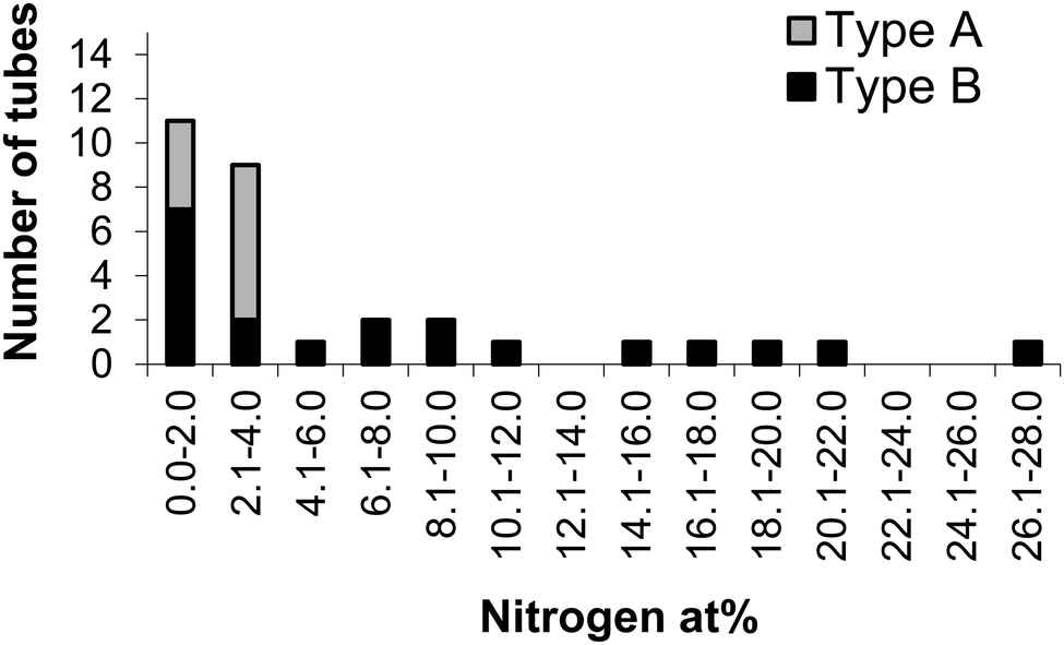 | ||
| Fig. 2 Nitrogen content of individual P,N-MWCNTs classified according to morphology. | ||
As well as using the intensity of the EELS edges for quantification, the structure of an edge can also provide information about the bonding environment of that element. K-edges arise from excitations of the 1s core electrons to unoccupied states with mainly p-like character. Changes in the bonding produce changes in the unoccupied states and π-bonded nitrogen results in a sharp feature, known as the π* peak, just after the edge onset at ∼400 eV. As the spectrum contains information about the bonding, changes in bonding as a result of beam irradiation can also be monitored. A series of spectra recorded from a Type A nanotube showed a slight decrease in nitrogen content (from 3.3 to 2.7 at%) over a seven minute period without any observable change in the nitrogen K-edge spectrum, an example of which is shown in Fig. 3a.
 | ||
| Fig. 3 Nitrogen K-edge from (a) a Type A nanotube, (b) a Type B nanotube and (c) an irradiated Type B nanotube. (d) The variation in nitrogen and carbon across a Type B nanotube, the shaded area marks the region where the EELS spectrum shows N2. | ||
In comparison to the typical Type A nanotube spectrum (Fig. 3a), the typical Type B spectrum (Fig. 3b) shows an increase in the nitrogen signal and a more pronounced π* peak. The variation in the carbon and nitrogen signals taken from a linescan across a Type B nanotube (Fig. 3d) shows that the nitrogen is mainly concentrated within the inner channel. Spectra from the center of the tube (pixels 8–10 on Fig. 3d) have a very pronounced π* peak indicating the presence of N2 gas (see ESI,† Fig. S4). At pixels 7 and 11, there is still a significant amount of nitrogen, but a large π* peak is not seen. The variation in the intensity and shape of the nitrogen K-edge is consistent with the inner channel containing N2 gas and the nitrogen bonding onto, or being contained within, the inner wall. N-MWCNTs10 and P,N-MWCNTs8 have both been previously reported to contain N2 gas. All except one of the nanotubes with >10% nitrogen appeared to contain N2 gas and it is likely that the one that did not had already been damaged by the electron beam. The ability to encapsulate N2 gas within the inner channel increases the nitrogen content of the Type B nanotubes compared to the Type A nanotubes.
Unlike the nitrogen K-edge from Type A nanotubes, the nitrogen edge from Type B nanotubes changes with beam irradiation. Comparison of spectra taken from several Type B nanotubes both before and after beam irradiation (e.g.Fig. 3b and c) show that there is an increase in the amount of nitrogen and a decrease in the π* peak. The structure of the Type B nanotubes was also found to change with beam irradiation; the first observable change being an increase in the amorphous layer on the inner wall of the nanotube. This amorphous layer can be seen in Fig. 1d and in high angle annular dark field (HAADF) and bright field images of the Type B nanotube shown in Fig. 4. An EELS line scan taken using a SMART acquisition9 along the line marked in 4a shows that this layer (marked region 2 on 4a) contains (bonded) nitrogen. The growth of this layer with exposure to the electron beam could be the result of a beam catalysed reaction between the N2 gas and the walls of the nanotube. The second observable stage of structural change involves the defined nanotube walls disappearing and the nanotube, which still contains nitrogen, becoming amorphous (see ESI,† Fig. S5). Trasobares et al.10 also found an increase in the nitrogen content with exposure to the electron beam for N-MWCNTs, although in their case they used the STEM probe to puncture the nanotube and an increase in the amount of N2 was seen before the N2 signal decreased significantly and then a bonded nitrogen signal appeared. In our case the nitrogen is incorporated into the structure rather than escaping from it.
 | ||
| Fig. 4 (a) HAADF and (b) bright field images of a Type B P,N-MWCNT containing a catalyst particle. The amorphous layer on the inside on the nanotube is indicated with an arrow in both images. The numbers 1, 2 and 3 in (a) indicate different regions of the line-scan. | ||
Our analysis of the connection between composition and morphology has focused on the nitrogen content of the nanotubes despite the nanotubes having been synthesized from precursors containing both nitrogen and phosphorus. This is because it has not been possible to detect a phosphorus EELS signal from the nanotubes but only from some of the catalyst particles, such as that shown in Fig. 4 (see also the ESI,† Fig. S6). Cruz-Silva et al.8 examined aerosol assisted CVD P,N-MWCNTs produced using different synthesis conditions to those studied here and observed phosphorous in the catalyst particles whilst finding that the amount of phosphorus present in the nanotube walls was below the detection limit of energy filtered TEM (EFTEM). Despite this, they argue that there was both a phosphorus signal and a nitrogen signal associated with the walls of a N2 gas containing nanotube during STEM experiments. The phosphorus was thought to be incorporated via P–N defects, as the defect energy is lower than that for a substitutional phosphorus defect (6.18 eV rather than 6.64 eV), although it is much higher than the energy of a substitutional nitrogen defect (0.73 eV).11 In our case, it has not been possible to detect a phosphorus signal from the nanotubes and we see nitrogen only on the inner surface or the inner layers of the wall for N2 containing nanotubes. Not only is the dopant concentration of the P,N-MWCNTs studied here different to those produced previously under different conditions, but in this case there are two different types of nanotube within the sample, each having a distinct composition and morphology.
For nanotubes produced using CVD, variations within the furnace12 (for example in temperature and gas composition) could be responsible for the different nanostructures and, by understanding the link, it is potentially possible to isolate individual morphologies resulting in samples with more uniform properties.
Along with the production of gas sensors, one of the motivations for incorporating phosphorus and nitrogen into nanotubes is to tailor the electronic properties for use in electrical applications. Understanding how the P,N-MWCNTs behave when current is passed is an important step towards achieving this goal. Previous work on N-MWCNTs with a bamboo structure has shown that the ∼3 at% nitrogen is removed during the restructuring, which results from Joule heating when current is passed.13 To investigate how the N2 gas containing nanotubes behave when current is passed, in situ experiments were carried out combining EELS and conductivity measurements. When current was passed though N2 gas containing nanotubes to obtain an IV curve, the N2 gas signal in the EELS fine structure was replaced by a bonded nitrogen signal. During the IV curve acquisition, the current was limited to 477 nA and so the amount of current needed to produce the bonded nitrogen is significantly less than that required to restructure the nanotube.
Current was then passed through a nanotube with a Type A section and a Type B section (Fig. 5a). The Type B section (marked area 2 on Fig. 5a) contained N2 gas (∼10 at% N), which, as before, became bonded when an IV curve was obtained. As applied bias, and corresponding current, was increased to 1600 mV and 77 μA, the nitrogen signal reduced significantly (to 2 at%) and the region of the nanotube restructured so that the internal and external diameters increased and the number of walls decreases, as shown in Fig. 5c. The Type A section (marked area 1 on Fig. 5a) showed no restructuring and the nitrogen content remained constant (∼2.5 at%, Fig. 5d). IV plots obtained before and after the current induced restructuring are shown in Fig. 5e.
 | ||
| Fig. 5 (a) P,N-MWCNT with a Type A (area 1) and a Type B (area 2) section. (b) Type B section before current flow. (c) Type B section after current flow. (d) EELS spectra of areas 1 and 2 before and after the initial IV spectra were taken. (e) IV curves before and after the current-induced restructuring of the nanotube. | ||
The Type A and Type B sections of the nanotube behaved differently when the same current was passed. Unlike the Type A section, the Type B section restructured and the nitrogen content decreased. Even with the same current flowing through them, the temperature achieved by Joule heating is likely to vary across the nanotube. The Type B section has fewer walls than the Type A section which means that the current density will be higher in the Type B section and we would expect a correspondingly higher temperature. Temperature variations may cause the two regions to behave differently. It is also possible that the Type B morphology can restructure more easily than the Type A, and that the reaction of the N2 with the nanotube may aid the restructuring process by, for example, creating defects on the nanotube walls.
Conclusions
P,N-MWCNT samples produced by CVD contain two different types of nanotube with distinct morphologies and chemical compositions. The first type of nanotube (Type A) contain stacked cone structures and have less than 4 at% nitrogen whilst the second type (Type B) are structures with a few walls which can encapsulate N2 gas and accommodate up to ∼30 at% nitrogen. The N2 gas reacts with the inner walls of the nanotube to produce bonded nitrogen when either subject to beam irradiation, or when current is passed. The phosphorus content was below the EELS detection limit for both types of tubes and was only detectable within the catalyst particles. The two different types of nanotube behave differently when current is passed, with the gas containing Type B nanotubes restructuring more readily than the cone-containing Type A nanotubes. Bulk nanomaterials, such as the P,N-MWCNT sample studied here, are an ensemble of individual nanostructures. The mechanism for producing different morphologies of nanotube within the same CVD MWCNT sample is still not fully understood, but it may be related to variations in the conditions within the furnace. If this is the case, isolation of the different morphologies could be possible resulting in samples with more uniform properties.Acknowledgements
We are grateful to the Engineering and Physical Sciences Research Council (Grant EP/H046550/1, EP/L022907/1 and EPSRC Pathways to Impact Awards), The Royal Society and the European Research Council (ERC) Starting Grant (ERC-2009-StG-240500 DEDIGROWTH; and ERC-2012-PoC 309786 DEVICE) for financial support. STEM experiments were performed at SuperSTEM, the EPSRC UK national facility for aberration-corrected STEM.Notes and references
- C. N. R. Rao and A. Govindaraj, Nanotubes and Nanowires, RSC Publishing, Cambridge, 2nd edn, 2011 Search PubMed.
- M. Penza, R. Rossi, M. Alvisi and E. Serra, Nanotechnology, 2010, 21, 105501 CrossRef CAS PubMed.
- M. Terrones, A. Jorio, M. Endo, A. Rao, Y. Kim and T. Hayashi, Mater. Today, 2004, 7, 30 CrossRef CAS.
- E. Cruz-Silva, F. Lopez-Urias, E. Munoz-Sandoval, B. G. Sumpter, H. Terrones, J.-C. Charlier, V. Meunier and M. Terrones, Nanoscale, 2011, 3, 1008 RSC.
- A. A. Koós, R. J. Nicholls, F. Dillon, K. Kertész, L. P. Biró, A. Crossley and N. Grobert, Carbon, 2012, 50, 2816 CrossRef PubMed.
- M. Glerup, M. Castignolles, M. Holzinger, G. Hug, A. Loiseau and P. Bernier, Chem. Commun., 2003, 2542 RSC.
- R. J. Nicholls, Z. Aslam, M. C. Sarahan, A. A. Koós, J. R. Yates, P. D. Nellist and N. Grobert, ACS Nano, 2012, 6, 7800 CrossRef CAS PubMed.
- E. Cruz-Silva, D. A. Cullen, L. Gu, J. M. Romo-Herrera, E. Muñoz-Sandoval, F. López-Urías, B. G. Sumpter, V. Meunier, J.-C. Charlier, D. J. Smith, H. Terrones and M. Terrones, ACS Nano, 2008, 2, 441 CrossRef CAS PubMed.
- K. Sader, B. Schaffer, G. Vaughan, R. Brydson, A. Brown and A. L. Bleloch, Ultramicroscopy, 2010, 110, 998 CrossRef CAS PubMed.
- S. Trasobares, O. Stephan, C. Colliex, G. Hug, W. K. Hsu, H. M. Kroto and D. R. M. Walton, Eur. Phys. J. B, 2001, 22, 117 CAS.
- E. Cruz-Silva, F. López-Urías, E. Muñoz-Sandoval, B. G. Sumpter, J.-C. Charlier, V. Meunier and M. Terrones, ACS Nano, 2009, 3, 1913 CrossRef CAS PubMed.
- S. S. Meysami, F. Dillon, A. A. Koós, Z. Aslam and N. Grobert, Carbon, 2013, 58, 151 CrossRef CAS PubMed.
- Z. Aslam, R. J. Nicholls, A. Koós, V. Nicolosi and N. Grobert, Adv. Funct. Mater., 2011, 21, 3933 CrossRef CAS.
Footnotes |
| † Electronic supplementary information (ESI) available: Larger versions of the images in Fig. S1a and d are shown in the ESI along with details of the proportion of Type A and Type B nanotubes within the sample, the variation in nitrogen content along the nanotubes, the presence of N2 gas in the inner channel of Type B nanotubes, beam irradiation of a Type B nanotube and the phosphorus signal from catalyst particles. See DOI: 10.1039/c4cp04272g |
| ‡ Present address: Institute for Materials Research, School of Chemical and Process Engineering (SCAPE), University of Leeds, Leeds LS2 9JT, UK. |
| § Present address: Nion Co., 1102 8th Street, Kirkland, WA 98033, USA. |
| ¶ Present address: Institute for Technical Physics and Materials Research, Hungarian Academy of Sciences, Hungary. |
| This journal is © the Owner Societies 2015 |