
 Open Access Article
 This Open Access Article is licensed under a Creative Commons Attribution-Non Commercial 3.0 Unported Licence
Visualization and deconvolution of carrier kinetics within grains of Cu2ZnSnS4−xSex using ultrafast diffuse reflectance microscopy†
Maha
Sharif
ab,
Xiao
Ma
ab and
Elham
Ghadiri
 *ab
*ab
aDepartment of Chemistry, Wake Forest University, Winston-Salem, 27109, North Carolina, USA. E-mail: ghadire@wfu.edu
bCenter for Functional Materials, Wake Forest University, Winston-, Salem, 27109, North Carolina, USA
First published on 15th July 2024
Abstract
Cu2ZnSnS4−xSex (x = 0–4, CZTSSe) materials are gaining interest for their solar energy conversion applications. We investigated the use of state-of-the-art ultrafast pump–probe microscopy and ultrafast image segmentation to visualize and spatially deconvolute photoexcited dynamics with CZTSSe materials at grain-size level. Band-tailing and electronic trap states are limitations in achieving high photovoltaic performance. We tested a combination of ultrafast pump–probe diffuse reflectance transient absorption microscopy (DR-TAM), and broadband femtosecond transient absorption spectroscopy in diffuse reflectance mode (DR-TAS) to understand the dynamic behaviors of charge carriers and sub-grain-resolved charge carrier kinetics in CZTSSe thin film-based devices. Broadband UV-NIR pulses have been used to monitor the photoexcited dynamics within grains of CZTSSe films under different UV and NIR photoexcitation wavelengths. Pump–probe microscopy showed spatially heterogeneous photoexcited patterns across different grains of CZTSSe films. Image segmentation analysis helped identify the type of photophysical processes at each grain and to determine whether the TAS signal therein consists of only one type of photophysical process or a combination of different transient absorption features including excited-state absorption (ESA), ground-state bleaching (GSB), or ESA/GSB spectral reshaping. UV- and NIR-photo-excitations compared the charge carrier dynamics (trapping and de-trapping or free carriers) under high and low energy (compared to the bandgap) photoexcitation conditions. We observed features of localizing states in both DR-TAM and DR-TAS at even 200 nm above the bandgap implying that the bandgap may be better defined as a mobility gap (similar to amorphous silicon). Our findings present a modern approach and toolbox for the visualization and detailed photophysical analysis of semiconductor materials that are important for energy conversion applications.
 Elham Ghadiri | Elham Ghadiri received her PhD in Nanoscience and Nanotechnology from Sharif University of Technology in 2010. She obtained a PhD in Chemistry in 2014 from Ecole Polytechnique Federal de Lausanne (EPFL) in Switzerland under the supervision of Professor Michael Grätzel and Professor Jacques Moser. She joined Prof. Warren S. Warren at Duke University as a postdoctoral researcher. In 2018, she became an Assistant Professor in the Department of Chemistry at Wake Forest University. Her expertise is in ultrafast laser microscopy-spectroscopy technique development, nanomaterials synthesis and device fabrication for solar energy conversion, optoelectronics and bioelectronics. She was awarded as the TERMIS-WFIRM young investigator of the tissue engineering and regenerative medicine international society in 2017. She earned the NSF CAREER award in 2023. |
1. Introduction
Pump–probe transient absorption spectroscopy (TAS) provides insights into ultrafast photophysical processes within materials, namely excited-state characteristics, the spectral signature of photocarriers absorption, charge separation, charge trapping, and charge recombination dynamics. Ultrafast transient absorption microscopy (TAM), which is a sub-class of pump–probe microscopy, is an advanced and powerful technique that facilities the visualization of the photophysical processes. The technique has been used (within its optical diffraction limits) to visualize the charge carrier transport within nanowires and to image pigments found at cultural heritage sites.1–4 Despite the great potential of conventional TAS, its main limitation is that it requires the samples to be optically transparent for the Beer–Lambert law to be applicable. Therefore, conventional transmission-based TAS is not suitable for the study of many opaque materials or highly light absorbing samples. We previously demonstrated an ultrafast time-resolved pump–probe diffuse reflectance spectrometer (DR-TAS) with a sub-200 fs time-resolution.5 The new technique enabled the understanding of ultrafast charge carrier separation in fully functional opaque dye-sensitized solar cells, highly light-absorbing, scattering materials, and new-generation Cu2BaSnS4−xSex (x = 0–4, CBTSSe). We integrated ultrafast TAM with diffuse reflectance spectroscopy (DR-TAM) to visualize the heterogeneous photophysical processes, namely the excited state pattern, with a spatial resolution of a few hundred nm to few µm (relevant to the grain size of advanced semiconductors used for photovoltaics).6,7The kesterite Cu2ZnSnS4−xSex (x = 0–4, CZTSSe) family has recently gained interest as an earth-abundant alternative to CuInxGa1−xSe28–10 and is a non-toxic substitute for CdTe11 that can be used in thin-film solar cells. Cu2ZnSnS4−xSex kesterite-based photovoltaic devices have made progress in conversion efficiency, from 6.7% for pure sulfide CZTS in 200912 to 12.6% for Se incorporated films CZTSSe in 201313 with a recent further improved efficiency to 13.8% in 2023.14 However, the main limitation of CZTSSe photovoltaics is the open circuit voltage (Voc), which remains far below the maximum achievable limit defined by the detailed balance limit.15 This has been attributed (although not fully understood) to different device performance-limiting mechanisms such as enhanced recombination due to tail states arising from Cu/Zn (or other cation) disorder,16–18 enhanced surface recombination at grain boundaries,19 and the influence of secondary phases.20 A detailed understanding of the photophysical processes such as electronic transitions, trap states, charge carrier generation kinetics, and recombination processes is essential for improving CZTSSe-based solar cell performance.
The photophysical characterization of larger bandgap CZTS materials using ultrafast laser techniques can be achieved in only a few studies, mainly those using intensity dependence or time-resolved photoluminescence (PL),21,22 transient absorption on single crystals,23 and terahertz measurements.24 PL spectroscopy can determine the lifetime of only radiative recombination between the carriers at the band edge or carriers localized in the donor and acceptor states. Excitation intensity dependent PL measurements show that the spectral shape of the PL strongly depends on the excitation intensity.21,22 At low excitation, luminescence occurs through defect-induced trap states within the bandgap of CZTS. Once the trap states are filled at higher excitation fluences, higher energy band-to-band emission becomes dominant, resulting in a shoulder in the upper energy region of the PL spectrum.21,22 In other words, the pronounced red-shift (∼100 meV) of the PL (compared to the band-edge determined from external quantum efficiency, EQE) for CZTSSe, and broadening of the PL is attributed to band tailing resulted from spatial bandgap or electrostatic potential variations in the film.16 While the PL experiments are reported to assess the radiative charge carrier recombination and distribution of electronic states, the non-radiative processes including the dynamics of the free photocarriers in the conduction and valence bands as well as the those of carriers localization or de-trapping within trap states remain unclear in CZTS or smaller bandgap CZTSSe thin films used in solar cells. Notably, CZTSSe chalcogenides exhibit exceptionally high optical absorption coefficients; hence, even thin films of this material appear dark with a relatively opaque color. This suggests that studies of the photophysical dynamics of this material can be performed more precisely using DR-TAM and DR-TAS.
In this study, we used ultrafast DR-TAM and DR-TAS to visualize the photoexcited processes in CZTS films. The charge generation was monitored within the grains using pump–probe microscopic imaging with a few hundred-nanometer spatial resolution. Our broadband TAS results revealed the existence of charge-localizing states and ultrafast trapping of charge carriers with de-trapping from these states occurring within tens of picoseconds. These states were observed even at ∼300 nm above the optical bandgap, indicating that the bandgap for this material may be better defined as a mobility gap (similar to amorphous silicon). As such, we used image segmentation to decompose and deconvolute the ultrafast images; the unique temporal and spatial sensitivity of microscopy enabled us to directly localize the fingerprints and dynamics of free carriers as well as carriers localized within electronic trap states at the sub-grain level.
2. Experimental
2.1. Materials and instrumentation
Cu (CH3COO)2 (99.99%), ZnCl2 (98%), SnCl2·2H2O (98%), thiourea (99.0%), and dimethyl sulfoxide (DMSO, 99.9%) were purchased from Sigma Aldrich (St. Louis, MO, USA) and used without further purification.The optical absorbance spectrum of samples was measured by an Agilent Cary 6000i UV-Vis-NIR spectrophotometer equipped with an integrating sphere (Agilent, DRA-1800![[thin space (1/6-em)]](https://www.rsc.org/images/entities/char_2009.gif) 150-mm diffuse reflectance external integrating sphere). SEM images were obtained using a Zeiss Gemini 300 while energy-dispersive X-ray spectroscopy (EDS) was obtained with a Bruker XFlash 6|30 Detector.
150-mm diffuse reflectance external integrating sphere). SEM images were obtained using a Zeiss Gemini 300 while energy-dispersive X-ray spectroscopy (EDS) was obtained with a Bruker XFlash 6|30 Detector.
2.2. Synthesis
CZTS/Se film was synthesized by annealing the molecular precursor based on (1) metal chalcogenides-hydrazine approach as developed by Mitzi et al.;13,25 and (2) Cu(CH3COO)2, ZnCl2, SnCl2·2H2O and thiourea in dimethyl sulfoxide (DMSO) as reported by Ki et al.26 For the DMSO approach, the mixed precursors including 0.8 mmol Cu(CH3COO)2, 0.56 mmol ZnCl2, 0.56 mmol SnCl2·2H2O, and 2.64 mmol thiourea (or 2:1.4:1.4:6.6 of Cu:Zn:Sn:S) were dissolved in 0.7 mL DMSO and stirred for 40 min. The solution turned into a transparent light-yellow color after the precursors were completely dissolved and was then drop-cast or spin-coated on a glass slide or Mo-coated glass substrates for heat treatment. Specifically, we pre-baked at 160 °C and annealed at 580 °C for 3 min. All the steps were performed in a nitrogen-filled glove box.
2.3. Ultrafast TAM and TAS
The ultrafast pump–probe transient absorption technique uses femtosecond pulses at 1030 nm, tunable at 1 kHz–100 kHz. The pump at different wavelengths relies on an optical parametric amplifier in tandem with a harmonic generator which allowed to use different pump beam at 460 nm, 600 nm, and 700 nm in different experiments. The probe beam was a white-light continuum generated in a sapphire plate with less energy than the pump on the sample to avoid multiple excitations. The pump and probe pulse length were ∼220 fs and the time resolution of measurements was approximately 350 fs (overlap time of the pump and probe). The pump pulses was modulated before the sample for pumpon and pumpoff measurements. The effective acquisition rate was typically 3 kHz, and a few thousand spectra were averaged to calculate each mean spectrum. The absorption change is calculated using eqn (1). | (1) |
pumped is given by the intensity of probe light reaching the detector through the sample that the pump pulses have not altered, and Ipumped is the intensity of light reaching the detector that the pump pulse has altered. The Ibackground refers to the intensity of the probe beam without interaction with the sample. The typical probe power was 400–800 µW, and pump power was typically 0.1–6 mW for the sample. With a pump power of 1 mW and a beam diameter of 5 µm the pump fluence was typically 50 mJ cm−2. With an absorption coefficient of 8.13 × 103 cm−1 and assuming a photon-to carrier yield of 100% for the CZTS sample, the initial carrier density was estimated 9.4 × 1020 cm−3 (calculations are provided in ESI†). For 600 nm-pump, T% become 5.61% and R% is 27.36%, α become 1.11/d = 7.4 × 103 cm−1 and the initial carrier density would become 11.2 × 1020 cm−3, which is 18.6% larger than the value for 460 nm-pump.
Satisfactory experimental condition is determined in control tests and considering sample thickness (absorbing power) and targeting a satisfactory signal to noise with considering the power limits to avoid photodegradation of samples. The photostability of the sample is tested by verifying if the signal is reproducible over several consecutive measurements. The broadband spectrum was acquired using a spectrograph-equipped photodiode array. The overlap time of pump and probe was wavelength-dependent owing to the chirp of the white light. We used a standard procedure for chirp correction; namely, we fitted the temporal responses with the cross-correlation function between the pump and supercontinuum probe to access the correct time-delay response for different wavelengths.
2.4. Density functional theory (DFT) electronic calculations and crystal structure
The crystal structure of CZTS (ICSD-12710)27 was plotted with VESTA,28 and the sizes of atoms were based on the Shannon Effective Ionic Radii.29 DFT calculations were performed with the aforementioned structure with CAmbridge Serial Total Energy Package (CASTEP)30 using the HSE06 hybrid exchange–correlation function for a more accurate bandgap estimation.3. Results
Based on the Shannon effective ionic radii,29 Cu+ and Zn2+ both have 0.6 angstroms radius (Fig. 1a), and their similar size and coordination leads to CuZn and ZnCu anti-site defects. The electronic structure (Fig. 1b) suggests CZTS is a direct band semiconductor with a bandgap of 1.23 eV (1008 nm). This value is lower than the bandgap derived from EQE and optical absorbance experimental results (1.45–1.51 eV; 851–821 nm).31–33 For the partial density of the states of CZTS, the valence band maximum is mainly formed by the 3d-orbital from Cu and 3p-orbital from S, and the conduction band minimum is normally contributed to the 5s-orbital of Sn and 3p-orbital of S. The Brillouin zone for Kesterite CZTS is provided in Fig. S1 (ESI†). The optical transmittance, reflectance, and absorptance spectra (Fig. 1c) shows the absorption edge (at ∼850 nm) IR region, which is characteristic to the CZTS band-edge transition and consistent with previous reports. | ||
| Fig. 1 Structural, electronic, optical, and microscopic characterization of the kesterite CZTS samples. The (a) crystal structure, and (b) calculated band structure and density of states (DOS) (HSE06 hybrid function) for the kesterite CZTS. (c) Total transmittance, total reflectance, and absorptance spectra for CZTS film. (d) XRD pattern for CZTS prepared using the DMSO approach. Scanning electron microscopy images using the (e) hydrazine, and (f) DMSO synthetic approaches. | ||
According to X-ray diffraction analysis of the CZTS sample prepared with DMSO approach (after annealing) (Fig. 1d), the characteristic peaks are consistent with the calculated pattern of the kesterite Cu2ZnSnS4. The EDS (Fig. S2, ESI†) was performed to reveal the atomic composition; the EDS of the film was measured as [Cu]/[Zn + Sn] = 1.16 and [Zn]/[Sn] = 0.95, which was consistent with their stoichiometric values, although S is relatively deficient. The SEM image of the CZTSSe film (Fig. 1e) reveals a grain size of approximately 500 nm to 3 µm for the sample prepared by the hydrazine approach with much smaller crystallites when using the DMSO approach for CZTS sample (Fig. 1f). The cross-section SEM image and the corresponding elemental distribution across the cross-section of CZTS film for which the optical response is presented in Fig. 1c, is provided in Fig. S4 (ESI†).
3.1. Pump–probe diffuse reflectance microscopic imaging of CZTSSe
In this context, TAM (a subclass of pump–probe microscopy) refers to pump–probe TAS under the microscopy configuration. In these experiments, the pump and probe beams collinearly passed through a microscope objective and, after interaction with the sample, the probe beam was directed to the detector using the second microscope objective. For diffuse reflectance measurements, the same objective was used for focusing and diffuse reflectance beam collection.In TAM images, the image contrasts consisted of excited state absorption (ESA), ground-state bleaching (GSB), and stimulated emission (SE). By convention, the reflectance change is calculated with and without pump excitation using the equation (−ΔR = Rprobenotpumped − Rprobepumped); ESA provides a positive-signed image contrast whereas GSB and SE result in negative-signed image contrasts. A positive signal indicates an increased photoinduced absorption while a negative signal indicates a decreased photoinduced absorption of the sample. The pump and probe are scanned on the sample to visualize the spatial variations. Additionally, the pump–probe time delay is changed; at each delay time, a pump–probe TAS microscopic image is acquired. It should be noted that in our control tests the same trend was observed in several measurements, and the pump–probe images and amplitude of the TAS signals were reproducible over consecutive measurements; this indicated a lack of sample photodegradation under this experimental condition.
Fig. 2a depicts the pump–probe TAM image of the CZTSSe film at 500 fs after excitation, which was at 700 nm. The TAM image was heterogeneously composed of positive and negative regions. The pump–probe signal averaged over the entire scan area compared with those from some example region of interest (ROI) is shown in Fig. 2b. Heterogeneity was also observed in the TAS signal kinetics extracted from different regions of the sample. Some grains showed a positive excited-state relaxation kinetics, some show negative bleaching recovery kinetics, and in some regions the signal evolves from negative to positive. The average TAS signal showed a bleach recovery within ∼60 ps, which evolves to excited state absorption. For quantitative comparison the time-traces were fitted with exponential decay or exponential growth functions and the fitting parameters are provided in Table 1. The time constants of the ESA relaxation are τ1 = 2.65 and τ2 = 20.8 ps and ps in ROI1. The τ1 time constant of exponential growth function fit for ROIs 2–5 has a value between 0.35 ps and 1.79 ps. The same trend is also observed for the τ2 component with value between 1 ps and 18 ps. The time constants for the evolution of the TAS signal averaged over the ensemble of grains are 0.73 ps and 11 ps (Table 1).
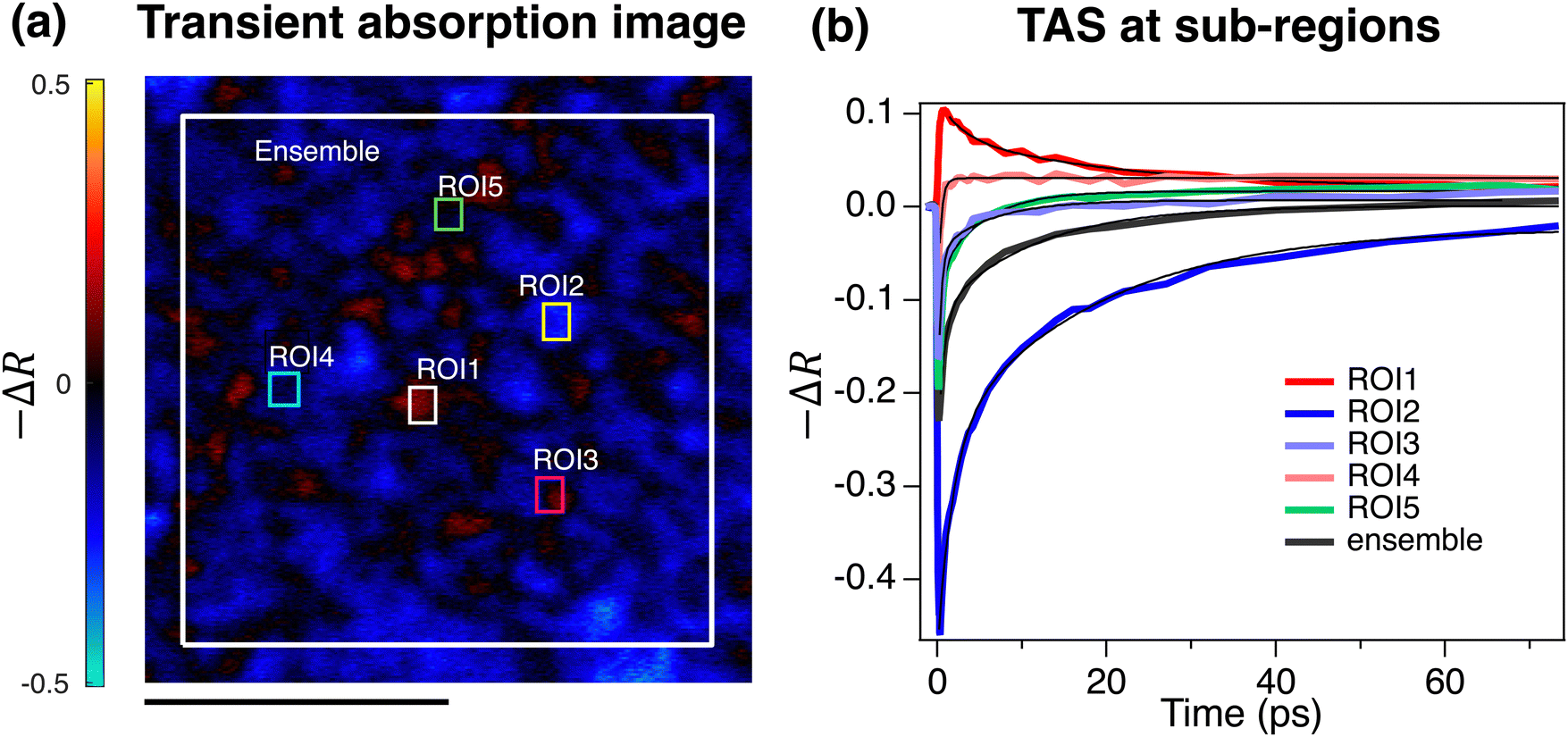 | ||
| Fig. 2 Pump–probe transient absorption microscopy of CZTSSe devices and the kinetics of charge carriers. Excitation was at 700 nm (above the bandgap) and probe beam was at 817 nm. (a) Pump–probe TAS image at 500 fs with an 18 µm × 18 µm field of view; scale bar shows 9 µm. (b) The TAS signal of different grains compared to the signal averaged over the scanned area is depicted. The experiments were performed in diffuse reflectance mode as the device was completely opaque. The pump and probe powers were 0.4 mW in both measurements. Solid lines are double-exponential function fit to TAS signals. | ||
| Y 0 | A 1 | τ 1 (ps) | A 2 | τ 2 (ps) | |
|---|---|---|---|---|---|
| ROI1 | 0.019 ± 0.003 | 0.039 ± 0.009 | 2.65 ± 0.89 | 0.058 ± 0.008 | 20.8 ± 4.1 |
| ROI2 | −0.023 ± 0.008 | −0.225 ± 0.018 | 1.79 ± 0.22 | −0.230 ± 0.017 | 18.0 ± 2.4 |
| ROI3 | 0.007 ± 0.002 | −0.181 ± 0.015 | 0.38 ± 0.05 | −0.055 ± 0.005 | 6.2 ± 1.1 |
| ROI4 | 0.035 ± 0.018 | −0.137 ± 0.014 | 0.36 ± 0.06 | −0.007 ± 0.011 | 1.1 ± 0.2 |
| ROI5 | 0.017 ± 0.001 | −0.216 ± 0.016 | 0.35 ± 0.04 | −0.092 ± 0.004 | 5.1 ± 0.4 |
| Ensemble | 0.001 ± 0.002 | −0.152 ± 0.010 | 0.73 ± 0.08 | −0.116 ± 0.005 | 11.0 ± 0.9 |
It is remarkable that photon energy of the probe at 820 nm (1.5 eV), is above the bandgap 1100 nm (1.13 eV) identified for CZTSSe films using EQE measurements.16,34 Therefore, the observation of negative regions is a measure of charge carriers trapped within electronic states extended above the bandgap. This resemble the electronic structure of amorphous materials same as amorphous silicon, for which a mobility gap was described.35 The mobility gap of amorphous films should be equal or larger than the band gap of the crystalline as a measure of the influence of lattice disorder on optical gap of the films.35 Electrostatic potential and band gap/compositional inhomogeneity across the films were previously reported by intensity and temperature-dependence photoluminescence (PL) and external quantum efficiency measurements. Although the exact mechanism of the defect transition in CZTS is not yet clearly understood, but spectral shifts of PL peaks at different temperature or excitation intensity was attributed to the presence of significant potential variations.36–38 It is noteworthy that the TAM microscopy image enabled to visualize the presence of these localizing states above the bandgap. Spatial bandgap or electrostatic potential fluctuations can cause such heterogeneity in TAM images and carrier kinetics across different grains.
3.2. Image principal component analysis
We performed principal component analysis (PCA) of the pump–probe TAM images of CZTS sample and identified a set of orthogonal-basis TAS signal components, referred to as principal components (PCs); these could be combined to reproduce the signal at any given pixel (Fig. 3). The PC signals are all at the same wavelength. In this method, the data matrix is divided into main principal components, according to the singular value decomposition analysis approach in which the principal (meaningful) parts of a matrix data are separated from the noise (also known as a noise reduction method).7,39 The composite TAM image was deconvoluted into three images shown in red, green, and blue with their corresponding TAS signal component provided next to each. PC1 was assigned to the excited state relaxation by minority charge carriers. PC2 represented the ground state bleaching from charge carriers localized within electronic states. PC3 was indicative of charge carriers that localized in electronic states; their relaxation (de-trapping) from these electronic states within a few picoseconds after excitation leads to the recovery of the bleach. The PC signal components were fitted with exponential growth or exponential decay functions and the fitting curves and fitting parameters are provided in Fig. S3 and Table S1 (ESI†). The time constant of PC1's relaxation (ESA relaxation) and PC’3 recovery (GSB recovery) is 31.25 ± 4.71 ps and 11.37 ± 0.62 ps respectively, and the time constant for PC2's GSB to ESA evolution is 8.25 ± 0.68 ps. Remarkably, the PCA facilitate to visualize and distinguish the photo-response of different grains and to know what grains show which type of behavior. | ||
| Fig. 3 Principal component analysis of the pump–probe TAM image of the CZTSSe devices and the kinetics of charge carriers. Representative false-color images of PC1 (red), PC2 (green), PC3 (blue), and the composite image (PC1 + PC2 + PC3) obtained by projection of PCs of the pump–probe image of the sample. The corresponding three PC signals are depicted. PC1 represent the excited state relaxation and its corresponding image identifies grains that show this kinetic behavior. PC2 and PC3 respectively represents the ground-state bleaching (localized charge carriers within electronic states) and ground state bleaching that recovers to excited state (de-trapping of charge carriers) and their corresponding image show grains with those kinetic behavior. | ||
Pump–probe experiments are typically carried out on large ensembles of particles or molecules, where the response of individual contributors combines with that from others to produce strong optical signals from the illuminated sample. For some heterogeneous samples, however, the response from individual components is lost when averaging over the ensemble. Such kinetic deconvolution is not straightforward using conventional ensemble spectroscopy, which is an ensemble measurement in which it cannot easily be ascertained whether a given signal is an averaged contribution of different components all existing at the same time or otherwise a homogeneous single component within the sample. Remarkably, the pump–probe TAM image spatially showed the excited state pattern over different grains, and the principal component image deconvolution analysis identified the type of photoexcited process at the grain-size level. The spatial heterogeneity in transient signals at different regions on the sample is explained in terms of spatial electronic variations. Red regions represent positive excited state optical absorption (by charge carriers) and negative regions (GSB) is a bleaching of probe due to population of electronic states. The presence of localizing electronic states is expected to affect the relaxation kinetics of charge carriers.
 | ||
| Fig. 4 Broadband diffuse reflectance pump–probe transient absorption spectra of CZTSSe thin films. Pump wavelength is 600 nm. The probe beam is a white light in the 700–900 nm spectral region. Different pump powers of (a) 300, (b) 500, and (c) 600 µW are applied. The probe power was kept constant at 20 µW. The samples are fully functional and opaque CZTSSe thin film-based devices, and the experiments were performed in diffuse reflectance mode. | ||
Several spectral features were noted in the broadband TAS spectrum. First, in the 700–780 nm region, an ultrafast negative peak formed and evolved into a positive peak in approximately 1.5 ps. Second, in the 780–880 nm region, a large and broad negative peak was observed; after some tens of picoseconds, the negative bleach diminished and a positive TAS peak appeared. By increasing the excitation power, the amplitude of the positive TAS in the 800–880 nm region (which appeared after several picoseconds) increased. Third, in the >880–900 nm region, another negative peak was observed. In the latest spectral region, the signal remained negative; the TAS spectrum reshaping was not observed even when increasing the excitation power. The large negative peak in the 800–880 nm region was due to GSB formed by photocarriers populating the higher energy extended states. The positive TAS can be attributed to the charge carrier's absorption with a lifetime of picoseconds. The amplitude of the positive feature attributed to the charge carrier absorption was larger at wavelengths below 750 nm where the spectral overlap with the carriers that are formed in the extended states (contributing to negative overlapping signal) was smaller. The bandgap of CZTSSe (prepared by the same method as the CZTSSe in this study) was estimated 1100 nm (1.13 eV) from EQE measurements. The PL peak for this material was reported with a pronounced red-shift at 1200 nm (1.03 eV).16,34 The negative bleaching peaks observed up to 800 nm spectral region (much higher energy compared to band-edge) is a direct evidence to assess the electronic states within this material and is also an indication that the bandgap for this material can be known as mobility gap same as amorphous silicon.35
The kinetics of the pump–probe TAS signals probed at different spectral regions are shown in Fig. 5. In Fig. 5a and b, the TAS signal measured at 736 nm and 779 nm are depicted until 100 ps and 30 ps, respectively. At a wavelength of 736 nm, the positive signal formed under a picosecond. As the negative bleaching signal was not present at 736 nm, the kinetic evolution of this signal reflects the pure relaxation of charge carriers. At 779 nm, however, a negative signal evolved to the ESA in 5 ps as the spectral evolution at this region was also evident in the broadband spectrum (Fig. 4). Fig. 5c shows the TAS kinetics recorded further in the NIR region. The bleaching kinetics observed at wavelengths 819 nm and 845 nm are longer-lived, which could be due to carriers localized in the extended states. The relaxation of the bleaching signal and conversion into positive TAS kinetics indicated the relaxation of localized carriers from these states and the formation of free charge carriers in 30–40 ps. At wavelengths of 865 nm (Fig. 5c) and 880–900 nm (Fig. 5d), the kinetics reflected pure photobleaching, which was a result of the carriers in the band edge tail remaining for 100 ps. We expected that the free carriers would absorb with the same amplitude in the entire 800–900 NIR region. If present, we ought to have observed their positive transient absorption signature across the entire 800–900 nm NIR region. However, the absence of free carrier absorption between 880 and 900 nm indicated that the carriers trapped in these states have a longer lifetime and do not delocalize within the time frames of our laser spectroscopy. Therefore, our broadband studies identified the spectral signature of two types of electronic traps, one in the 800–880 nm range and another in the 880–900 nm range.
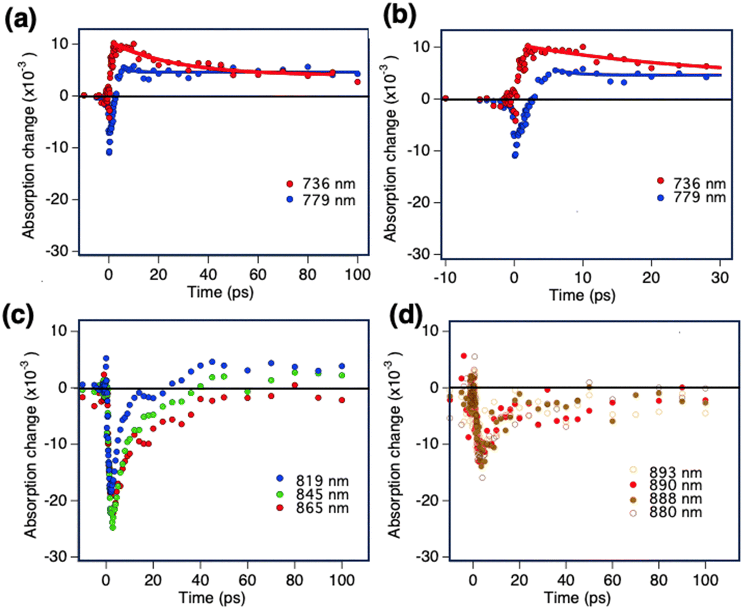 | ||
| Fig. 5 Photo-induced transient absorption kinetics for NIR-excited CZTSSe devices measured in diffuse reflectance modes. The pump wavelength was 600 nm. (a) and (b) TAS kinetics recorded in the 730–780 nm range up to 100 and 30 ps. (c) The TAS kinetics from the 800–860 nm region, and (d) the TAS kinetics further in the NIR region close to the band edge of the CZTSSe. The samples are fully functional opaque CZTSSe devices, and the experiments are performed in diffuse reflectance mode. | ||
The combination of different bleaching types of signal at spectral regions up to ∼300 nm above the optical bandgap strongly suggests that the electronic bandgap for CZTSSe materials may be better defined as a mobility gap similar to amorphous silicon, and also points to the existence of the bandgap (and potential fluctuations) within the film grains.
 | ||
| Fig. 6 Time-resolved broadband TAS spectra and TAS relaxation kinetics for UV-excited CZTS. (a) Time-resolved TAS broadband spectra, and (b) The TAS kinetics at different spectral region. The sample is excited at 460 nm and probed using white light pulses in the 550–900 spectral range. Solid lines correspond to biexponential fit with fitting parameters shown in Table 2. | ||
| λ (nm)/parameters | 550 | 600 | 650 | 700 | 750 | 819 |
|---|---|---|---|---|---|---|
| Y 0 | 0.42 ± 0.00 | 0.32 ± 0.00 | 0.217 ± 0.00 | 0.16 ± 0.00 | 0.13 ± 0.00 | 0.10 ± 0.00 |
| A 1 | 0.33 ± 0.04 | 0.34 ± 0.02 | 0.48 ± 0.03 | 0.56 ± 0.03 | 0.60 ± 0.03 | 0.64 ± 0.05 |
| τ 1 (ps) | 2.57 ± 0.54 | 1.65 ± 0.23 | 0.81 ± 0.08 | 0.72 ± 0.06 | 0.70 ± 0.05 | 0.53 ± 0.06 |
| A 2 | 0.26 ± 0.02 | 0.24 ± 0.01 | 0.22 ± 0.01 | 0.19 ± 0.01 | 0.18 ± 0.01 | 0.18 ± 0.01 |
| τ 2 (ps) | 24.62 ± 3.37 | 19.42 ± 1.99 | 14.49 ± 1.11 | 12.88 ± 0.97 | 13.07 ± 1.02 | 12.86 ± 1.19 |
Different kinetic behaviors at spectral regions that were closer to or further away from the band edge were also observed at low-energy NIR excitations. Probing at 700 nm for both NIR and UV excitations, a positive relaxing ESA signal was observed, albeit with different relaxation rates. At probe wavelength regions above 800 nm, NIR excitations resulted in the trapping of carriers within electronic states, and their de-trapping was associated with the emergence of excited state absorption after tens of picoseconds. Meanwhile, UV excitations initially resulted in positive photoexcited absorption by photocarriers that relaxed in tens of picoseconds.
4. Discussion and conclusion
We analyzed the kinetics of charge carrier processes within electronic and trap states of CZTS/Se semiconductors using ultrafast TAM and TAS. Using principal component analysis image decomposition, we extracted 3 kinetic components, and spatially and kinetically deconvoluted the TAM image into 3 TAM image components. This analysis helps identify the photophysical processes at each grain and assists in understanding whether the TAS signal at each grain consists of only one type of photophysical process or a combination of different transient absorption features (ESA, GSB, or ESA/GSB spectral reshaping).The broadband TAS results upon NIR photoexcitation show broad GSB peaks from 900 nm extending up to 800 nm. Considering the bandgap of the CZTSSe sample (1097 nm as determined from the optical absorbance spectrum and DFT calculations) the observed bleaching up to 800 nm indicates the existence of localizing electronic states energetically above the optical bandgap. This suggests the presence of extended trap states at the band edge. The existence of electronic states in CZTS/Se materials was previously shown by non-time-resolved temperature-dependence PL spectroscopy. Our ultrafast spectroscopy results shed light on the photophysics of these materials by demonstrating the ultrafast behavior of photoexcited carriers at broad spectral regions when excited closer to band edge using NIR pulses or at energies above the band edge using UV pulses.
In the CZTSSe samples, the free charge carriers (measured optimally in the spectral region of approximately 730 nm to avoid signal bleaching) are stable up to hundreds of picoseconds. When the CZTSSe thin films are measured at the probe wavelength of 817 nm, the signal polarization changes from negative to positive in a few picoseconds. It is not straightforward to determine the mechanism of this polarization change using ensemble spectroscopy if it is originating from the trapping and de-trapping of carriers in this time frame, is a contribution from optical effects such as the refractive index or has another origin. The pump–probe microscopy results supported by ensemble spectroscopy can localize the type of charge carriers (trapped and free) within the grains of a few micrometers in size. The spatial resolution of the pump–probe microscopy allows us to localize the charge carriers within 200–400 nm.6,7 Using TAM and PCA deconvolution of TAM when probing at 817 nm (above the bandgap), we observed that a minority of grains showed an ESA signal (originating from free carrier's absorption) while the majority showed a GSB type of signal (originating from trapped carriers). Using image kinetic deconvolution of TAM, we observed some of the trapped carriers would delocalize into ESA but others remain within electronic states (deconvoluted PC remains negative). The average signal over the entire scanned area showed the same type of negative-to-positive evolution and in agreement with ensemble spectroscopy. Therefore, the deconvoluted subregion kinetics indicate that the signal polarization change was due to an averaging effect over subregions and different photophysical responses across different grains.
Our broadband measurements supported by the TAM observations showed an entirely different spectral and kinetic components in the CZTSSe samples with CBTSSe films.6,7 For CBTSSe, the carrier kinetics measured at 817 nm, relaxed faster, and had a lifetime of several picoseconds. Additionally, the electronic states were less extended in the CBTSSe compared with CZTSSe. From pump–probe imaging, we could detect the local variation in the effective potential due to inhomogeneity in stoichiometry. In the broadband spectrum of the CBTSSe samples, the photo-bleaching component was relatively narrow and located at the band edge transition with relatively minimal contribution from the extended higher energy levels. The heterogeneity in TAS images was due to local stoichiometry inhomogeneity that resulted in local energetic variation in different grains. These observations are another indication of the sharp energy transition caused by less extended states in CBTSSe compared to the extended states of CZTSSe.
Data availability
The data supporting this article have been included as part of the ESI.†Conflicts of interest
There are no conflicts to declare.Acknowledgements
Financial support from NSF (CHE) under award 2239539 is greatly acknowledged. E. Ghadiri acknowledge D. Mitzi for fruitful discussions.References
- M. M. Gabriel, E. M. Grumstrup, J. R. Kirschbrown, C. W. Pinion, J. D. Christesen, D. F. Zigler, E. E. M. Cating, J. F. Cahoon and J. M. Papanikolas, Imaging Charge Separation and Carrier Recombination in Nanowire P-i-n Junctions Using Ultrafast Microscopy, Nano Lett., 2014, 14(6), 3079–3087, DOI:10.1021/nl5012118.
- E. M. Grumstrup, M. M. Gabriel, E. E. M. Cating, E. M. Van Goethem and J. M. Papanikolas, Pump–Probe Microscopy: Visualization and Spectroscopy of Ultrafast Dynamics at the Nanoscale, Chem. Phys., 2015, 458, 30–40, DOI:10.1016/j.chemphys.2015.07.006.
- T. E. Villafana, W. P. Brown, J. K. Delaney, M. Palmer, W. S. Warren and M. C. Fischer, Femtosecond Pump–Probe Microscopy Generates Virtual Cross-Sections in Historic Artwork, Proc. Natl. Acad. Sci. U. S. A., 2014, 111(5), 1708–1713, DOI:10.1073/pnas.1317230111.
- Z. Guo, J. S. Manser, Y. Wan, P. V. Kamat and L. Huang, Spatial and Temporal Imaging of Long-Range Charge Transport in Perovskite Thin Films by Ultrafast Microscopy, Nat. Commun., 2015, 6(1), 7471, DOI:10.1038/ncomms8471.
- E. Ghadiri, S. M. Zakeeruddin, A. Hagfeldt, M. Grätzel and J.-E. Moser, Ultrafast Charge Separation Dynamics in Opaque, Operational Dye-Sensitized Solar Cells Revealed by Femtosecond Diffuse Reflectance Spectroscopy, Sci. Rep., 2016, 6(1), 24465, DOI:10.1038/srep24465.
- E. Ghadiri, D. Shin, A. Shafiee, W. S. Warren and D. B. Mitzi, Grain-Resolved Ultrafast Photophysics in Cu2BaSnS4–x Sex Semiconductors Using Pump–Probe Diffuse Reflectance Spectroscopy and Microscopy, ACS Appl. Mater. Interfaces, 2018, 10(46), 39615–39623, DOI:10.1021/acsami.8b12307.
- H. Luebbering, A. Shafiee, B. Teymur, Y. Kim, D. B. Mitzi and E. Ghadiri, Ultrafast Microscopy and Image Segmentation of Spatially Heterogeneous Excited State and Trap Passivation in Cu2BaSnSSe3, Cell Rep. Phys. Sci., 2023, 101601, DOI:10.1016/j.xcrp.2023.101601.
- P. Jackson, D. Hariskos, R. Wuerz, O. Kiowski, A. Bauer, T. M. Friedlmeier and M. Powalla, Properties of Cu(In,Ga)Se2 Solar Cells with New Record Efficiencies up to 21.7%, Phys. Status Solidi RRL, 2015, 9(1), 28–31, DOI:10.1002/pssr.201409520.
- P. Jackson, R. Wuerz, D. Hariskos, E. Lotter, W. Witte and M. Powalla, Effects of Heavy Alkali Elements in Cu(In,Ga)Se2 Solar Cells with Efficiencies up to 22.6%, Phys. Status Solidi RRL, 2016, 10(8), 583–586, DOI:10.1002/pssr.201600199.
- A. Chirilă, P. Reinhard, F. Pianezzi, P. Bloesch, A. R. Uhl, C. Fella, L. Kranz, D. Keller, C. Gretener, H. Hagendorfer, D. Jaeger, R. Erni, S. Nishiwaki, S. Buecheler and A. N. Tiwari, Potassium-Induced Surface Modification of Cu(In,Ga)Se2 Thin Films for High-Efficiency Solar Cells, Nat. Mater., 2013, 12(12), 1107–1111, DOI:10.1038/nmat3789.
- D. Shin, B. Saparov and D. B. Mitzi, Defect Engineering in Multinary Earth-Abundant Chalcogenide Photovoltaic Materials, Adv. Energy Mater., 2017, 7(11), 1602366, DOI:10.1002/aenm.201602366.
- H. Katagiri, K. Jimbo, W. S. Maw, K. Oishi, M. Yamazaki, H. Araki and A. Takeuchi, Development of CZTS-Based Thin Film Solar Cells, Thin Solid Films, 2009, 517(7), 2455–2460, DOI:10.1016/j.tsf.2008.11.002.
- W. Wang, M. T. Winkler, O. Gunawan, T. Gokmen, T. K. Todorov, Y. Zhu and D. B. Mitzi, Device Characteristics of CZTSSe Thin-Film Solar Cells with 12.6% Efficiency, Adv. Energy Mater., 2014, 4(7), 1301465, DOI:10.1002/aenm.201301465.
- M. A. Green, E. D. Dunlop, M. Yoshita, N. Kopidakis, K. Bothe, G. Siefer and X. Hao, Solar Cell Efficiency Tables (Version 63), Prog. Photovolt. Res. Appl., 2024, 32(1), 3–13, DOI:10.1002/pip.3750.
- J. W. Shockley, Detailed Balance Limit of Efficiency of P–n Junction Solar Cells, 2024.
- T. Gokmen, O. Gunawan, T. K. Todorov and D. B. Mitzi, Band Tailing and Efficiency Limitation in Kesterite Solar Cells, Appl. Phys. Lett., 2013, 103(10), 103506, DOI:10.1063/1.4820250.
- J. J. S. Scragg, J. K. Larsen, M. Kumar, C. Persson, J. Sendler, S. Siebentritt and C. Platzer Björkman, Cu–Zn Disorder and Band Gap Fluctuations in Cu2ZnSn(S,Se)4: Theoretical and Experimental Investigations, Phys. Status Solidi B, 2016, 253(2), 247–254, DOI:10.1002/pssb.201552530.
- J. J. S. Scragg, L. Choubrac, A. Lafond, T. Ericson and C. Platzer-Björkman, A Low-Temperature Order-Disorder Transition in Cu2ZnSnS 4 Thin Films, Appl. Phys. Lett., 2014, 104(4), 041911, DOI:10.1063/1.4863685.
- D. B. Mitzi, O. Gunawan, T. K. Todorov, K. Wang and S. Guha, The Path towards a High-Performance Solution-Processed Kesterite Solar Cell, Sol. Energy Mater. Sol. Cells, 2011, 95(6), 1421–1436, DOI:10.1016/j.solmat.2010.11.028.
- S. Siebentritt, Why Are Kesterite Solar Cells Not 20% Efficient?, Thin Solid Films, 2013, 535, 1–4, DOI:10.1016/j.tsf.2012.12.089.
- T. Gershon, B. Shin, T. Gokmen, S. Lu, N. Bojarczuk and S. Guha, Relationship between Cu 2 ZnSnS 4 Quasi Donor-Acceptor Pair Density and Solar Cell Efficiency, Appl. Phys. Lett., 2013, 103(19), 193903, DOI:10.1063/1.4829920.
- T. M. Ng, M. T. Weller, G. P. Kissling, L. M. Peter, P. Dale, F. Babbe, J. De Wild, B. Wenger, H. J. Snaith and D. Lane, Optoelectronic and Spectroscopic Characterization of Vapour-Transport Grown Cu 2 ZnSnS 4 Single Crystals, J. Mater. Chem. A, 2017, 5(3), 1192–1200, 10.1039/C6TA09817G.
- L. Quang Phuong, M. Okano, Y. Yamada, A. Nagaoka, K. Yoshino and Y. Kanemitsu, Photocarrier Localization and Recombination Dynamics in Cu2ZnSnS4 Single Crystals, Appl. Phys. Lett., 2013, 103(19), 191902, DOI:10.1063/1.4829063.
- G. W. Guglietta, K. R. Choudhury, J. V. Caspar and J. B. Baxter, Employing Time-Resolved Terahertz Spectroscopy to Analyze Carrier Dynamics in Thin-Film Cu2ZnSn(S,Se)4 Absorber Layers, Appl. Phys. Lett., 2014, 104(25), 253901, DOI:10.1063/1.4884817.
- D. A. R. Barkhouse, O. Gunawan, T. Gokmen, T. K. Todorov and D. B. Mitzi, Device Characteristics of a 10.1% Hydrazine-Processed Cu2ZnSn(Se,S)4 Solar Cell, Prog. Photovoltaics Res. Appl., 2012, 20(1), 6–11, DOI:10.1002/pip.1160.
- W. Ki and H. W. Hillhouse, Earth-Abundant Element Photovoltaics Directly from Soluble Precursors with High Yield Using a Non-Toxic Solvent, Adv. Energy Mater., 2011, 1(5), 732–735, DOI:10.1002/aenm.201100140.
- S. Schorr, H.-J. Hoebler and M. Tovar, A Neutron Diffraction Study of the Stannite-Kesterite Solid Solution Series, Eur. J. Mineral., 2007, 19(1), 65–73, DOI:10.1127/0935-1221/2007/0019-0065.
- K. Momma and F. Izumi, VESTA 3 for Three-Dimensional Visualization of Crystal, Volumetric and Morphology Data, J. Appl. Crystallogr., 2011, 44(6), 1272–1276, DOI:10.1107/S0021889811038970.
- R. D. Shannon, Revised Effective Ionic Radii and Systematic Studies of Interatomic Distances in Halides and Chalcogenides, Acta Crystallogr., Sect. A: Cryst. Phys., Diffr., Theor. Gen. Crystallogr., 1976, 32(5), 751–767, DOI:10.1107/S0567739476001551.
- S. J. Clark, M. D. Segall, C. J. Pickard, P. J. Hasnip, M. I. J. Probert, K. Refson and M. C. Payne, First Principles Methods Using CASTEP, Z. Kristallogr. – Cryst. Mater., 2005, 220(5–6), 567–570, DOI:10.1524/zkri.220.5.567.65075.
- H. Katagiri, N. Sasaguchi, S. Hando, S. Hoshino, J. Ohashi and T. Yokota, Preparation and Evaluation of Cu2ZnSnS4 Thin Films by Sulfurization of E□B Evaporated Precursors, Sol. Energy Mater. Sol. Cells, 1997, 49(1–4), 407–414, DOI:10.1016/S0927-0248(97)00119-0.
- B. Shin, O. Gunawan, Y. Zhu, N. A. Bojarczuk, S. J. Chey and S. Guha, Thin Film Solar Cell with 8.4% Power Conversion Efficiency Using an Earth-abundant Cu 2 ZnSnS 4 Absorber, Prog. Photovoltaics Res. Appl., 2013, 21(1), 72–76, DOI:10.1002/pip.1174.
- D. B. Mitzi, O. Gunawan, T. K. Todorov, K. Wang and S. Guha, The Path towards a High-Performance Solution-Processed Kesterite Solar Cell, Sol. Energy Mater. Sol. Cells, 2011, 95(6), 1421–1436, DOI:10.1016/j.solmat.2010.11.028.
- W. Wang, M. T. Winkler, O. Gunawan, T. Gokmen, T. K. Todorov, Y. Zhu and D. B. Mitzi, Device Characteristics of CZTSSe Thin-Film Solar Cells with 12.6% Efficiency, Adv. Energy Mater., 2014, 4(7), 1301465, DOI:10.1002/aenm.201301465.
- F. D. Quarto; F. D. Franco; A. Zaffora and M. Santamaria, Photocurrent Spectroscopy in Passivity Studies, Encyclopedia of Interfacial Chemistry, 2018, pp. 361–371 Search PubMed.
- B. Teymur, S. Levcenco, H. Hempel, E. Bergmann, J. A. Márquez, L. Choubrac, I. G. Hill, T. Unold and D. B. Mitzi, Optoelectronic and Material Properties of Solution-Processed Earth-Abundant Cu2BaSn(S, Se)4 Films for Solar Cell Applications, Nano Energy, 2021, 80, 105556, DOI:10.1016/j.nanoen.2020.105556.
- M. Lang, C. Zimmermann, C. Krämmer, T. Renz, C. Huber, H. Kalt and M. Hetterich, Luminescence Properties of Cu2ZnSn (S, Se)4 Solar Cell Absorbers: State Filling versus Screening of Electrostatic Potential Fluctuations, Phys. Rev. B, 2017, 95(15), 155202, DOI:10.1103/PhysRevB.95.155202.
- S. Kretzschmar, S. Levcenco, J. Just, A. Redinger and T. Unold, Radiative Recombination from Localized States in CZT(S, Se) Investigated by Combined PL and TRPL at Low Temperatures, in 2016 IEEE 43rd Photovoltaic Specialists Conference (PVSC); IEEE: Portland, OR, USA, 2016; pp 0169–0172 DOI:10.1109/PVSC.2016.7749571.
- M. DeMarco, M. Ballard, E. Grage, F. Nourigheimasi, L. Getter, A. Shafiee and E. Ghadiri, Enhanced Photochemical Activity and Ultrafast Photocarrier Dynamics in Sustainable Synthetic Melanin Nanoparticle-Based Donor–Acceptor Inkjet-Printed Molecular Junctions, Nanoscale, 2023, 15(35), 14346–14364, 10.1039/D3NR02387G.
Footnote |
| † Electronic supplementary information (ESI) available. See DOI: https://doi.org/10.1039/d4tc01512f |
| This journal is © The Royal Society of Chemistry 2024 |