
High synaptic plasticity enabled by controlled ion migration in organic heterojunction memristors†
Yangzhou
Qian
a,
Jiayu
Li
ab,
Wen
Li
 *a,
Cheng-Hung
Hou
c,
Ziyi
Feng
a,
Wei
Shi
*d and
Mingdong
Yi
*a
*a,
Cheng-Hung
Hou
c,
Ziyi
Feng
a,
Wei
Shi
*d and
Mingdong
Yi
*a
aState Key Laboratory of Organic Electronics and Information Displays, Jiangsu Key Laboratory for Biosensors, Institute of Advanced Materials (IAM), Nanjing University of Posts & Telecommunications (NUPT), Nanjing 210023, China. E-mail: iamwli@njupt.edu.cn; iammdyi@njupt.edu.cn
bCollege of Electronic and Optical Engineering & College of Flexible Electronics (Future Technology), Jiangsu Province Engineering Research Center for Fabrication and Application of Special Optical Fiber Materials and Devices, Nanjing University of Posts and Telecommunications (NUPT), Nanjing 210023, China
cResearch Center for Applied Sciences Academia Sinica, Taipei 11529, Taiwan
dKey Laboratory of Flexible Electronics and Institute of Advanced Materials, Nanjing Tech University, Nanjing 211816, China. E-mail: iamwshi@njtech.edu.cn
First published on 6th June 2024
Abstract
Organic memristors with uniform resistive switching behavior can mimic the functions of biological synapses, making them promising candidates for brain-inspired neuromorphic computing. Among these, organic memristors based on ion migration mechanisms have been widely studied because of the directional movement of anions such as metal cations and oxygen ions under electric fields, which is more similar to the biological process of ion release in synapses. However, controlling these ion dynamic processes is often challenging, with rapid ion migration leading to unstable device performance and reduced accuracy. Here, we present the fabrication of a memristor utilizing an organic heterojunction. The built-in electric field generated by the heterojunction slows down and orders the ion migration process, enabling the device to exhibit a wide range of precise multiple conductive states (10−6–10−3 A). This provides an advantage in simulating synaptic behavior. The continuously adjustable conductance in organic heterojunction memristors successfully mimics various forms of synaptic plasticity, including paired-pulse facilitation (PPF), post-tetanic potentiation (PTP), short-term plasticity (STP) and long-term plasticity (LTP), as well as higher-order functionalities such as simulating Pavlovian classical conditioning reflex experiment and experiential learning function. Furthermore, by utilizing X-ray photoelectron spectroscopy (XPS) and time-of-flight secondary-ion mass spectrometry (ToF-SIMS) depth profiling, we have gained clear insights into the distribution and movement of ions of different compositions within the device, elucidating the underlying reasons for resistance changes. These findings provide reliable references and demonstrations for the design and control of future ion migration-type memristors.
 Wen Li | Wen Li, currently an associate professor at Nanjing University of Posts and Telecommunications (NUPT), completed her PhD in organic electronics at NUPT's Institute of Advanced Materials (IAM) in 2017, with joint training at Imperial College London from 2015 to 2016. Following her doctoral studies, she conducted postdoctoral research at Northwestern Polytechnical University in China and the University of Oxford in the UK. Returning to IAM at NUPT in 2020, her research has focused on high-performance thin-film transistors, organic semiconductor memory devices, and energy-efficient organic neuromorphic electronics. She was awarded the Jiangsu Association for Science and Technology's Young Scientific Talent Support Program (2023). |
Introduction
Memristors play a vital role in artificial neural networks, owing to their unique non-linear resistance values, making them crucial components for enhancing the efficiency of machine learning and artificial intelligence.1–3 Through memristors, neural networks can achieve efficient computation and storage, thereby improving throughput and energy efficiency.4–11 Their programmability and multi-conductance characteristics enable memristors to adapt to various neural network structures and application requirements, facilitating precise model training and inference. Additionally, memristors can also enable low-power, high-performance real-time processing in edge computing scenarios, providing critical support for the application of artificial intelligence technologies in fields such as smartphones and the Internet-of-Things (IoT).12–15 To ensure the uniformity and accuracy of memristive networks, memristors typically require a large dynamic range of conductivity and high precision programmability, posing higher demands on memristors.Ion migration is a typical mechanism in memristors, where ions in the material or electrode migrate under the action of an electric field, leading to changes in the device's resistance values, thus realizing multiple discrete conductive states, hence memristors based on ion migration mechanism are usually analogue memristors with continuous change of device conductance.16,17 In addition, this process is very similar to the biological process of ion release in synapses and offers advantages such as fast response, low energy consumption, high density, and reconfigurability, and thus have attracted significant interests.18–21 Among them, memristors using organic materials as the ion migration active layer demonstrate unique advantages, as they can introduce an oxide layer at the metal–organic interface to serve as the source of ions, providing active oxygen ions.22–24 However, these ion dynamics processes are often difficult to control,25–27 leading to unstable device performance. How to control ions to move uniformly and orderly, achieving a wide range of high-precision conductive states, remains a challenge.
Based on this, we propose an organic heterojunction memristor (OHM), which achieves controllable and stable ion migration by constructing an organic heterojunction to realize multi-conductive state analog memristors. Heterojunctions effectively stabilize the lattice and suppress rapid ion migration.28–30 The heterojunction of OHM is composed of p-type pentacene and n-type N,N′-ditridecylperylene-3,4,9,10-tetracarboxylic diimide (P13). The built-in electric field generated by the heterojunction allows the ion migration process to proceed slowly and orderly, enabling the device to achieve a wide range (10−6–10−3 A) and high-precision conductive states. The continuously tunable conductance of OHM has high plasticity and can realize various basic synaptic functions, including paired-pulse facilitation (PPF), post-tetanic potentiation (PTP), short-term plasticity (STP) and long-term plasticity (LTP), as well as simulations of higher-order functions, including Pavlovian classical conditioning reflex experiment and experiential learning function. Through X-ray photoelectron spectroscopy (XPS) and time-of-flight secondary-ion mass spectrometry (ToF-SIMS) depth profiling, the distribution and movement of anions and cations inside the device are clearly observed, revealing the underlying reasons for the resistance changes in OHMs. This research is expected to provide valuable insights for the design and control of ion migration-type memristors.
Experimental section
Device fabrications
Pentacene and N,N′-ditridecylperylene-3,4,9,10-tetracarboxylic diimide (P13) were purchased from Sigma-Aldirch Co., Ltd and used without further purification. All OHMs were fabricated in a configuration of ITO/Pentacene/P13/Al, in which a 20-nm-thick Pentacene and 20-nm-thick P13 films were deposited on an ITO-coated glass substrate in a vacuum chamber to form heterojunction, respectively. Before this the glass substrate with ITO strip electrodes was cleaned by acetone, ethanol, and deionized water for 10 min each, and then baked in an oven at 120 °C for 30 min, followed by UV-ozone treatment for 10 min. Al top electrodes were finally thermally evaporated onto the heterojunction layer through patterned shadow masks (strip type: 100, 250, 500, and 1000 μm) in a vacuum (≈10−4 Pa). The thickness of each evaporated layer was monitored in real time in a vacuum chamber by a quartz crystal vibrometer.Electrical measurement
All electrical characterizations of the device were performed in ambient air using a probe station and a Keithley 4200 s semiconductor parameter analyzer system equipped with our programming test software. The voltage signals designed for specific learning rules were applied to the ITO electrode, and the Al electrode is grounded.Material characterizations
Optical absorption spectra of the active layer were collected by UV-vis spectrowemeter (PerkinElmer Lambda35). UPS data were recorded by the XPS/UPS photoelectron spectrometer (*/KRATOS Axis Supra). c-AFM measurements were performed in contact mode in ambient air using Bruker's Dimension Icon AFM with an SCM-PIC type probe tip. The parameters of PIC probe tip are shown as follows: tip material (0.01–0.025 Ω cm antimony (n) doped Si), cantilever (T: 1.8 μm, L: 450 μm, W: 35 μm), fo: 10 kHz, k: 0.1 N m−1, coating (front side: conductive Pt/Ir, back side: reflective Pt/Ir). All XPS depth profiles were acquired using a PHI 5000 VersaProbe (ULVAC-PHI) system. During XPS depth profiling, a monochromatic Al Kα X-ray with a beam diameter of 100 μm was utilized to produce characteristic photoelectrons, and a 1 keV Ar+ ion beam was used as the etching source. To compensate the surface charge, 10 eV electron and Ar+ ion were simultaneously applied on the sample surface during data acquisitions. All ToF-SIMS depth profiles were acquired using a PHI TRIFT V nanoTOF (ULVAC-PHI) system with a dual beam slice-and-view scheme. During the spectrum acquisition phase, a pulsed 20-keV C60+ (pulse frequency of 8200 Hz and pulse length of 15 ns) ion beam was chosen as the primary ion beam to minimize the surface damage. During spectrum acquisitions, pulsed 10 eV electron and Ar+ ion flooding were applied to compensate for the surface charge. During the sputter phase, 1 keV Ar+ ion beam was applied as the etching source.Results and discussion
The structure of Organic Heterojunction Memristor (OHM) is illustrated in Fig. 1a, where 20 nm of pentacene and 20 nm of P13 are sequentially vacuum-deposited on a glass substrate with etched stripe ITO electrodes. Subsequently, aluminum electrodes are formed through shadow mask evaporation to create a cross-bar configuration, with device dimensions of 100 μm × 100 μm. The molecular structures of pentacene and P13 are depicted in Fig. 1b. Studying the energy band structure of heterojunctions is crucial for understanding the formation of local built-in electric fields and the transport of charge carriers. The energy levels of pentacene and P13 were calculated by UPS and UV-vis, as shown in Fig. S1 (ESI†). The highest occupied molecular orbital (HOMO) of P13 is 0.4 eV lower than that of pentacene (Fig. 1c), resulting in an organic pn junction. Its built-in electric field helps improve the ion migration process, leading to a wider range of conductivity in the device, and ensuring uniform and stable conductivity changes. Typical current–voltage (I–V) characteristics of the device under positive and negative voltage scanning cycles are shown in the left and right halves of Fig. 1d, respectively. Under positive bias scanning (0 V → +10 V → 0 V), the conductivity of the device gradually increases. Conversely, applying a continuous negative bias voltage (0 V→ −10 V → 0 V) leads to a gradual decrease in conductivity. Fig. S2 (ESI†) shows the current values at the end of each scan, up to 160 cycles of I–V curve scanning, with a gradual increase in current values. At +10 V, the current increases from 2.1 × 10⁻⁶ A to 1.5 × 10⁻³ A, an approximately 3 orders of magnitude amplification. This wide range, high-precision conductive state gives OHM a significant advantage in simulating synaptic plasticity. Additionally, the I–V characteristics of the heterojunction device were examined using atomic force microscopy (c-AFM) measurements (Fig. 1e). ITO-coated glass substrates serve as the bottom common electrode, the heterojunction as the middle layer, and Pt-coated c-AFM tip as the top electrode. c-AFM measurements were conducted in contact mode, covering a sample area of 3 μm × 3 μm.31–33 Clear current responses were observed at +10 V and −10 V, consistent with the actual OHM I–V characterization results. Furthermore, tests were conducted on the current maps of the film surface under different scanning voltage frequencies, as shown in Fig. S3 (ESI†). It can be observed that the current on the film surface is not significant at low voltages, with significant positive current appearing at +8 V and negative current at −7 V. The electrical characteristics of the nanoscale-scaled devices are consistent with those observed in actual memristors. This suggests tunable conductivity of OHM depending on voltage polarity and magnitude. c-AFM characterization not only rules out filamentary switching mechanisms within the device but also demonstrates the potential of OHM to be reduced to tens of nanometers for high-density integration.34,35 Additionally, the impact of scan rate on the OHM was investigated, as shown in Fig. S4 (ESI†). As the scan rate increases, the hysteresis area of the I–V curve decreases, indicating that changing the scan rate can effectively modulate the resistance. Therefore, the appropriate scan rate forms the basis for achieving desirable resistance variation.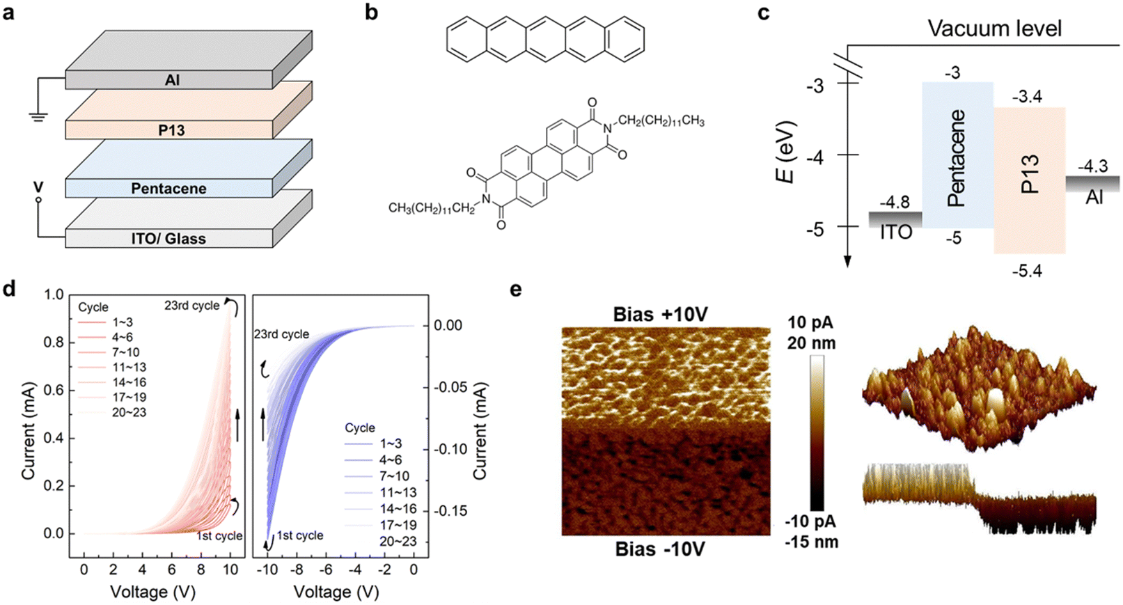 | ||
| Fig. 1 Schematics of (a) two-terminal OHM in ITO/Pentacene/P13/Al configuration and (b) molecular structure of Pentacene and P13. (c) Energy band diagram of OHM. (d) I–V characteristics of the OHM respond to positive (left) and negative (right) voltage sweeps. (e) c-AFM measurements of OHM: current mappings of heterojunction film under voltage sweep of +10 V (upper) and −10 V (bottom). The images on the right are 3D AFM and 3D c-AFM current mapping of the heterojunction film, respectively. | ||
More characterizations were carried out to help understand the resistive switching mechanism. First, we measured the area dependence I–V characteristics for OHM device. Fig. S5 (ESI†) shows the cell area dependence of currents in the devices with different areas ranging from 100 × 100 to 100 × 1000 μm2. We note that the resistance change process is continuous rather than filamentary.36 Next, previous researches have shown that the aluminum electrode and ITO electrode can generate mobile O2− and In+ ions under an electric field, respectively.25,26 X-ray photoelectron spectroscopy (XPS) depth profiling can determine the elemental composition and content of the device from surface to interior by ion sputtering. Fig. 2a–c show the results of initial state, low resistance state (LRS), and high resistance state (HRS) tests, where the sputtering time corresponds to the depth of the device The distribution of Al, C, and In elements in the initial device allow for the clear identification of the Al electrode, organic heterojunction layer, and ITO structure. Due to the susceptibility of the Al electrode to oxidation, AlOx is commonly present in the Al electrode.37–39 After applying the +10 V voltage treatment, the LRS of the memristor could be achieved. It can be observed that the O element significantly increases in the organic layer, while the proportion of C element content decreases substantially. The intrusion of In elements into the organic heterojunction layer leads to a uniform decrease in concentration gradient from ITO to the Al/organic interface. This clearly indicates the migration of O2− and In+ ions, with the increase in ion concentration in the organic layer resulting in the device transitioning to LRS. Applying the −10 V voltage returns the device to HRS. At this point, the content of AlOx in the organic layer increases. This is attributed to the migration of Al3+ ions towards the organic layer under reverse voltage, causing the distribution of AlOx in the organic layer. Meanwhile, some In+ ions retract to the ITO. These processes lead to OHM returning to HRS. Furthermore, the XPS spectra of Al 2p (Fig. 2d–f) and In 3d (Fig. 2g–i) were analyzed under the three conditions of the initial state, LRS, and HRS. Al 2p was divided into AlOx and metallic Al components, while In 3d was divided into In 3d3/2 and In 3d5/2 components, with the sputtering time from the surface to the interior representing depth. It can be clearly observed that in LRS devices, In elements diffuse from the bottom ITO to the organic layer, and in HRS devices, the content of AlOx in the organic layer increases. These results indicate that ion movement in the organic heterojunction under an electric field is the fundamental cause of OHM resistance change. The I–V curves of single-layer pentacene and P13 devices exhibit a linear relationship (Fig. S6, ESI†), indicating the importance of heterojunction structure. The organic heterojunction not only provides channels for the migration of these ions but also effectively slows down the rate of ion migration through its built-in electric field, enabling the continuous and orderly migration of ions, thereby endowing OHM with a wide range and high precision of conductive states.
 | ||
| Fig. 2 XPS depth profiles of the OHM in (a) initial state, (b) LRS, and (c) HRS. Al 2p XPS spectrum (d)–(f) and In 3d XPS spectrum (g)–(i) acquired at different depths from the initial state, LRS, and HRS, respectively. | ||
Finally, we employed time-of-flight secondary-ion mass spectrometry (ToF-SIMS) to provide a more intuitive and clearer confirmation of ion migration behavior within the device. ToF-SIMS provides chemical state and molecular information of elements on the surface of solid materials, making it an advanced surface analysis technique and an important tool for surface and interface detection. ToF-SIMS can reconstruct a three-dimensional chemical structure model of the sample at nanometer resolution, allowing for a more intuitive and clear display of the changes in chemical composition and content within the device.40,41 In order to visualize the dynamic process of ion migration within the device more intuitively and clearly, the thickness of both pentacene and P13 was increased to 80 nm, thereby increasing the thickness of the organic heterojunction layer, and devices with an area of 250 μm × 250 μm were prepared for measurement. Fig. 3a–c show the three-dimensional structures of the devices in their initial state, LRS and HRS, as well as the three-dimensional models of individual components. The results are consistent with those obtained from XPS analysis. Positive voltage causes significant diffusion of inorganic ions within the organic layer of LRS devices, weakening the isolation of the organic layer from the top and bottom electrodes, resulting in nearly overlapping three-dimensional models of the electrodes. Conversely, reverse voltage partially reverses the migration of these ions. Fig. S7 (ESI†) displays the ToF-SIMS 3D images of each element in the OHM in its initial state, LRS, and HRS. Fig. 3d–f quantitatively illustrate the distribution and content of internal components of the devices under the three states. It can be observed from the figures that the distribution range of pentacene and P13 within the device narrows and they tend to aggregate towards the bottom ITO, with a decrease in their relative proportions. These results, together with XPS testing, collectively confirm the ion migration process within OHM, and ToF-SIMS analysis provides a clearer and more intuitive method for elucidating the mechanism of resistive switching devices.
 | ||
| Fig. 3 ToF-SIMS 3D images (a)–(c) and depth profiles (d)–(f) of OHM in initial state, LRS, and HRS, respectively. | ||
In biological neural networks, synapses are the points of connection between two neurons (Fig. 4a). During the process of information transmission, the presynaptic membrane of one neuron releases neurotransmitters, which alter the ion channel selectivity of the postsynaptic membrane of the subsequent neuron, leading to changes in membrane potential. This results in excitatory postsynaptic currents (EPSCs) or inhibitory postsynaptic currents (IPSCs). Fig. S8 (ESI†) illustrates a typical EPSC. In this process, the strength of synaptic connections changes, which is known as synaptic plasticity.42,43 Based on the duration of maintenance, synaptic plasticity can be classified into short-term plasticity (STP) and long-term plasticity (LTP).44,45 Paired-pulse facilitation (PPF) is a typical form of STP. When two consecutive stimuli reach the synapse, the second stimulus elicits a larger EPSC (Fig. S9, ESI†). The enhancement effect of PPF is dependent on time interval, with shorter intervals resulting in stronger enhancement.46,47 This is attributed to the residual neurotransmitters present in the synapse. Similar to PPF, post-tetanic potentiation (PTP) is defined as the persistent change in synaptic plasticity following a series of stimuli, which is also dependent on time interval. We examined the index of PPF and PTP synaptic functions in OHM, respectively, according to the equations as follows
| PPF = (I2 − I1)/I1 × 100% | (1) |
| PTP = (I10 − I1)/I1 × 100% | (2) |
 | ||
| Fig. 4 (a) Schematic illustration of neuron and synapse. (b) Extracted PPF and PTP index versus impulse interval Δt, where I1, I2, and I10 are the recorded current after the first, second, and tenth input spike, respectively. (c) Current responses to 20 identical stimulation pulses (+10 V, 50 ms) at different frequencies (0.1–2.5 Hz). (d) STP–LTP transition. LTP were triggered by applying consecutive spikes (N = 5–50, V = +10 V, ΔT = 50 ms), where ΔT denotes spike duration. The retention data recorded at a read voltage of +1 V. (e) Schematic of ANN consists of 784 input neurons. The input image can be divided into 28 × 28 input information for input neurons. (f) Relationship between recognition rates and training iterations. The inset shows LTP and LTD data, from which linearity (NL), maximum conductance (Gmax), and minimum conductance (Gmin) were extracted as input parameters for neural network training. (g) Simulation of Pavlov's classical conditioned reflex experiment. (h) A 5 × 5 OHM array demonstrated memory plasticity, with regions A, B, and C corresponding to initial learning (+10 V), active memory clearing (−10 V), and relearning (+10 V), respectively, with pixel-level values representing different memory intensities. | ||
In addition to the aforementioned basic synaptic plasticity simulations, OHMs have successfully achieved higher-order synaptic functionalities. Firstly, through LTP and long-term depression (LTD), image recognition training was conducted. An artificial neural network (ANN) was simulated based on the Modified National Institute of Standards and Technology (MNIST) dataset of handwritten digits.50,51 The ANN comprises a three-layer neural network with 28 × 28 input neurons, 100 hidden neurons, and 10 output neurons,52 depicted in Fig. 4e. The recognition accuracy increased with the training epoch, approaching 95% (Fig. 4f). The inset of Fig. 4f shows LTP and LTD data, from which linearity (NL), maximum conductance (Gmax), and minimum conductance (Gmin) were extracted as input parameters for neural network training. A smaller linearity (NL) is essential for achieving high recognition accuracy. Secondly, we simulated Pavlov's classical conditioning experiment.53 A −3 V voltage stimulus served as the conditioned stimulus (CS) bell sound, while a +10 V voltage stimulus served as the unconditioned stimulus (US) food, with a 0.2 mA threshold current used to determine whether the dog salivates (Fig. 4g). Initially, the food induced salivation in the dog, while the bell did not. With the association training of the bell and food, the dog established a connection between the bell and food, subsequently salivating upon hearing the bell, although this memory gradually weakened over time. This experiment demonstrates the excellent learning ability and memory retention of OHM. Based on this, the learning-forgetting-relearning behavior of the human brain was simulated.54,55 The device current was normalized to represent the strength of memory as synaptic weights, as shown in Fig S12 (ESI†). Despite spontaneous forgetting leading to memory weakening, relearning quickly reawakens memories, thereby requiring shorter learning processes. Finally, the outstanding memory plasticity of our OHM was demonstrated in a 5 × 5 array, as displayed in Fig. 4h. Regions A, B, and C correspond to initial learning (+10 V), active memory erasure (−10 V), and relearning (+10 V), visualized as pixel values representing different memory intensities. These results underscore the excellent memory programmability of our OHM, making it a promising candidate for artificial synapses and edge computing.
Conclusion
In conclusion, through the construction of organic heterojunctions, we have achieved OHMs with controllable ion migration and high synaptic plasticity. XPS and ToF-SIMS depth profiling clearly observed the distribution and movement of mobile ions within the device, providing deep insights into the reasons for the resistance variation within OHMs. Furthermore, the local built-in electric field generated by organic heterojunctions allows for the slow and sustained migration of ions, enabling the device to achieve a wide range and high precision of tunable conductive states. OHMs successfully simulated various forms of synaptic plasticity, including PPF, STP, and LTP, as well as Pavlov's classical conditioning experiment and the learning-forgetting-relearning process. These studies highlight the tremendous potential of organic heterojunctions in memristive devices, offering an effective approach for high performance memristive device components.Author contributions
Y. Q. investigation, validation, formal analysis, data curation, methodology, writing original draft; J. L. validation, data curation, methodology; W. L. investigation, supervision, methodology; C. H. validation, data curation; Z. F. data curation; W. S. conceptualization, supervision; M. Y. conceptualization, supervision, resources.Conflicts of interest
There are no conflicts to declare.Acknowledgements
The project was financially supported by the National Natural Science Foundation of China (51933005, 62174089, 62275130, 62375125) and Postgraduate Research & Practice Innovation Program of Jiangsu Province (KYCX21_0776).References
- L. Chua, IEEE Trans. Circuit Theory, 1971, 18, 507–519 Search PubMed
.
- I. Valov, R. Waser, J. R. Jameson and M. N. Kozicki, Nanotechnology, 2011, 22, 254003 CrossRef PubMed
- Y. Yang and R. Huang, Nat. Electron., 2018, 1, 274–287 CrossRef
- Y. Yu, M. Xiao, D. Fieser, W. Zhou and A. Hu, J. Mater. Chem. C, 2024, 12, 3770–3810 RSC
- M. Rao, H. Tang, J. Wu, W. Song, M. Zhang, W. Yin, Y. Zhou, F. Kiani, B. Chen, X. Jiang, H. Liu, H.-Y. Chen, R. Midya, F. Ye, H. Jiang, Z. Wang, M. Wu, M. Hu, H. Wang, Q. Xia, N. Ge, J. Li and J. J. Yang, Nature, 2023, 615, 823–829 CrossRef CAS PubMed
- M. Lanza, A. Sebastian, W. D. Lu, M. L. Gallo, M.-F. Chang, D. Akinwande, F. M. Puglisi, H. N. Alshareef, M. Liu and J. B. Roldan, Science, 2022, 376, eabj9979 CrossRef CAS PubMed
- W. Zhang, B. Gao, J. Tang, P. Yao, S. Yu, M.-F. Chang, H.-J. Yoo, H. Qian and H. Wu, Nat. Electron., 2020, 3, 371–382 CrossRef
- M. A. Zidan, J. P. Strachan and W. D. Lu, Nat. Electron., 2018, 1, 22–29 CrossRef
- S. Jung, H. Lee, S. Myung, H. Kim, S. K. Yoon, S. W. Kwon, Y. Ju, M. Kim, W. Yi, S. Han, B. Kwon, B. Seo, K. Lee, G. H. Koh, K. Lee, Y. Song, C. Choi, D. Ham and S. J. Kim, Nature, 2022, 601, 211–216 CrossRef CAS PubMed
- S. Chen, M. R. Mahmoodi, Y. Shi, C. Mahata, B. Yuan, X. Liang, C. Wen, F. Hui, D. Akinwande, D. B. Strukov and M. Lanza, Nat. Electron., 2020, 3, 638–645 CrossRef CAS
- E. J. Fuller, S. T. Keene, A. Melianas, Z. Wang, S. Agarwal, Y. Li, Y. Tuchman, C. D. James, M. J. Marinella, J. J. Yang, A. Salleo and A. A. Talin, Science, 2019, 364, 570–574 CrossRef CAS PubMed
- D. H. Lim, S. Wu, R. Zhao, J. H. Lee, H. Jeong and L. P. Shi, Nat. Commun., 2021, 12, 319 CrossRef CAS PubMed
- P. Yao, H. Wu, B. Gao, J. Tang, Q. Zhang, W. Zhang, J. J. Yang and H. Qian, Nature, 2020, 577, 641–646 CrossRef CAS PubMed
- C. Choi, H. Kim, J. H. Kang, M. K. Song, H. Yeon, C. S. Chang, J. M. Suh, J. Shin, K. Lu, B. I. Park, Y. Kim, H. E. Lee, D. Lee, J. Lee, I. Jang, S. Pang, K. Ryu, S. H. Bae, Y. Nie, H. S. Kum, M. C. Park, S. Lee, H. J. Kim, H. Wu, P. Lin and J. Kim, Nat. Electron., 2022, 5, 386–393 CrossRef
- X. Xu, Y. Ding, S. X. Hu, M. Niemier, J. Cong, Y. Hu and Y. Shi, Nat. Electron., 2018, 1, 216–222 CrossRef
- C. Zhang, W. B. Ye, K. Zhou, H. Y. Chen, J. Q. Yang, G. Ding, X. Chen, Y. Zhou, L. Zhou, F. Li and S.-T. Han, Adv. Funct. Mater., 2019, 29, 1808783 CrossRef
- J. Lao, W. Xu, C. Jiang, N. Zhong, B. Tian, H. Lin, C. Luo, J. Travas-sejdic, H. Peng and C.-G. Duan, J. Mater. Chem. C, 2021, 9, 5706–5712 RSC
- V. Marx, Nature, 2014, 515, 293–297 CrossRef CAS PubMed
- Y. Yang, X. Zhang, L. Qin, Q. Zeng, X. Qiu and R. Huang, Nat. Commun., 2017, 8, 15173 CrossRef PubMed
- K. Lu, X. Li, Q. Sun, X. Pang, J. Chen, T. Minari, X. Liu and Y. Song, Mater. Horiz., 2021, 8, 447–470 RSC
- H. Wei, H. Yu, J. Gong, M. Ma, H. Han, Y. Ni, S. Zhang and W. Tao, Adv. Funct. Mater., 2021, 31, 2007232 CrossRef CAS
- Z. Wang, L. Wang, Y. Wu, L. Bian, M. Nagai, R. Jv, L. Xie, H. Ling, Q. Li, H. Bian, M. Yi, N. Shi, X. Liu and W. Huang, Adv. Mater., 2021, 33, 2104370 CrossRef CAS PubMed
- S. P. Park, Y. J. Tak, H. J. Kim, J. H. Lee, H. Yoo and H. J. Kim, Adv. Mater., 2018, 30, 1800722 CrossRef PubMed
- J. Li, Y. Qian, W. Li, S. Yu, Y. Ke, H. Qian, Y.-H. Lin, C.-H. Hou, J.-J. Shyue, Y. Chen, J. Zhou, J. Xu, J. Zhu, M. Yi and W. Huang, Adv. Mater., 2023, 35, 2209728 CrossRef CAS PubMed
- F. Xu, L. Wu, Q. Meng, M. Kaltak, J. Huang, J. L. Durham, M. Fernandez-Serra, L. Sun, A. C. Marschilok, E. S. Takeuchi, K. J. Takeuchi, M. S. Hybertsen and Y. Zhu, Nat. Commun., 2017, 8, 15400 CrossRef CAS PubMed
- M. Chi, C. Wang, Y. Lei, G. Wang, D. Li, K. L. More, A. Lupini, L. F. Allard, N. M. Markovic and V. R. Stamenkovic, Nat. Commun., 2015, 6, 8925 CrossRef CAS PubMed
- Z. He, L.-G. Chang, Y. Lin, F.-L. Shi, Z.-D. Li, J.-L. Wang, Y. Li, R. Wang, Q.-X. Chen, Y.-Y. Lu, Q.-H. Zhang, L. Gu, Y. Ni, J.-W. Liu, J.-B. Wu and S.-H. Yu, J. Am. Chem. Soc., 2020, 142, 7968–7975 CrossRef CAS PubMed
- Y. Xu, Y. Li, G. Peng, Q. Wang, Z. Li, H. Wang, G. Wang and Z. Jin, IEEE Electron Device Lett., 2022, 43, 1709–1712 CAS
- X. Zhang, D. Chu, B. Jia, Z. Zhao, J. Pi, Z. Yang, Y. Li, J. Hao, R. Shi, X. Dong, Y. Liang, J. Feng, A. Najar, Y. Liu and S. (Frank) Liu, Adv. Mater., 2024, 36, 2305513 CrossRef CAS PubMed
- W. Zhu, Z. Zhang, D. Chen, W. Chai, D. Chen, J. Zhang, C. Zhang and Y. Hao, Nano-Micro Lett., 2020, 12, 1–14 CrossRef PubMed
- G. Ding, Y. Wang, G. Zhang, K. Zhou, K. Zeng, Z. Li, Y. Zhou, C. Zhang, X. Chen and S.-T. Han, Adv. Funct. Mater., 2019, 29, 1806637 CrossRef
- Z. Y. Lv, Q. K. Hu, Z. X. Xu, J. J. Wang, Z. H. Chen, Y. Wang, M. Chen, K. Zhou, Y. Zhou and S.-T. Han, Adv. Electron. Mater., 2019, 5, 1800793 CrossRef
- J.-Y. Mao, L. Zhou, Y. Ren, J.-Q. Yang, C.-L. Chang, H.-C. Lin, H.-H. Chou, S.-R. Zhang, Y. Zhou and S.-T. Han, J. Mater. Chem. C, 2019, 7, 1491–1501 RSC
- Y. Aoki, C. Wiemann, V. Feyer, H. S. Kim, C. M. Schneider, H. Ill-Yoo and M. Martin, Nat. Commun., 2014, 5, 3473 CrossRef PubMed
- J. C. Scott and L. D. Bozano, Adv. Mater., 2007, 19, 1452 CrossRef CAS
- Z. Wang, F. Zeng, J. Yang, C. Chen and F. Pan, ACS Appl. Mater. Interfaces, 2012, 4, 447–453 CrossRef CAS PubMed
- M. Cölle, M. Büchel and D. M. de Leeuw, Org. Electron., 2006, 7, 305–312 CrossRef
- A. Kumatani, Y. Li, P. Darmawan, T. Minari and K. Tsukagoshi, Sci. Rep., 2013, 3, 1026 CrossRef PubMed
- R. K. Hart, Proc. R. Soc. London, Ser. A, 1956, A236, 68–88 Search PubMed
- W. Gardner, A. L. Hook, M. R. Alexander, D. Ballabio, S. M. Cutts, B. W. Muir and P. J. Pigram, Anal. Chem., 2020, 92, 6587–6597 CrossRef CAS PubMed
- A. Priebe, E. Huszar, M. Nowicki, L. Pethö and J. Michler, Anal. Chem., 2021, 93, 10261–10271 CrossRef CAS PubMed
- Y. van de Burgt, A. Melianas, S. T. Keene, G. Malliaras and A. Salleo, Nat. Electron., 2018, 1, 386–397 CrossRef
- C. Wu, T. W. Kim, H. Y. Choi, D. B. Strukov and J. J. Yang, Nat. Commun., 2017, 8, 752 CrossRef PubMed
- A. Citri and R. C. Malenka, Neuropsychopharmacology, 2008, 33, 18–41 CrossRef PubMed
- Y. Wang, Z. Lv, J. Chen, Z. Wang, Y. Zhou, L. Zhou, X. Chen and S.-T. Han, Adv. Mater., 2018, 30, 1802883 CrossRef PubMed
- W. Xu, H. Cho, Y. H. Kim, Y. T. Kim, C. Wolf, C. G. Park and T. W. Lee, Adv. Mater., 2016, 28, 5916 CrossRef CAS PubMed
- B. Li, Y. Q. Liu, C. J. Wan, Z. Y. Liu, M. Wang, D. P. Qi, J. C. Yu, P. Q. Cai, M. Xiao, Y. Zeng and X. D. Chen, Adv. Mater., 2018, 30, 1706395 CrossRef PubMed
- S. Brenowitz, J. David and L. Trussell, Neuron, 1998, 20, 135–141 CrossRef CAS PubMed
- R. S. Zucker and W. G. Regehr, Annu. Rev. Physiol., 2002, 64, 355–405 CrossRef CAS PubMed
- X. Xiong, J. Kang, Q. Hu, C. Gu, T. Gao, X. Li and Y. Wu, Adv. Funct. Mater., 2020, 30, 1909645 CrossRef CAS
- B. Cai, Y. Huang, L. Tang, T. Wang, C. Wang, Q. Sun, D. W. Zhang and L. Chen, Adv. Funct. Mater., 2023, 33, 2306272 CrossRef CAS
- X. Shan, C. Zhao, X. Wang, Z. Wang, S. Fu, Y. Lin, T. Zeng, X. Zhao, H. Xu, X. Zhang and Y. Liu, Adv. Sci., 2022, 9, 2104632 CrossRef CAS PubMed
- M. S. Fanselow and A. M. Poulos, Annu. Rev. Psychol., 2005, 56, 207–234 CrossRef PubMed
- G. Liu, C. Wang, W. Zhang, L. Pan, C. Zhang, X. Yang, F. Fan, Y. Chen and R.-W. Li, Adv. Electron. Mater., 2016, 2, 1500298 CrossRef
- Y. Park and J. S. Lee, ACS Nano, 2017, 11, 8962–8969 CrossRef CAS PubMed
Footnote |
| † Electronic supplementary information (ESI) available. See DOI: https://doi.org/10.1039/d4tc01257g |
| This journal is © The Royal Society of Chemistry 2024 |