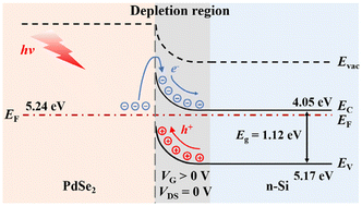
There is great interest in the incorporation of novel two-dimensional materials into Si-based technologies to realize multifunctional optoelectronic devices via heterogeneous integration. Here, we demonstrate a gate-tunable, self-driven, high-performance broadband phototransistor array based on a PdSe2/Si Schottky junction, which is fabricated by pre-depositing a semi-metallic PdSe2 film on a SOI substrate. In addition, thanks to the zero bandgap of the PdSe2 material and the PdSe2/Si vertical heterostructure, the prepared phototransistor exhibits pronounced photovoltaic properties in a wide spectral range from ultraviolet to near-infrared. The responsivity, specific detectivity and response time of the device at the incident light wavelength of 808 nm are 1.15 A W−1, 9.39 × 10¹⁰ Jones, and 27.1/40.3 μs, respectively, which are better than those of previously reported PdSe2-based photodetectors. The photoelectric performance can be further improved by applying an appropriate gate voltage to the phototransistor and the responsivity of the device increases to 1.61 A W−1 at VG = 5 V. We demonstrate the excellent imaging capabilities of a 4 × 4 array image sensor using PdSe2/SOI phototransistors under 375 nm, 532 nm, and 808 nm laser sources.
