
A focused ion beam-fabricated high-performance electrodeposited nickel–ruthenium–ruthenium oxide nano-supercapacitor†
Sudipta Biswas a,
Ahiud Moragbc,
Nitzan Shauloffa,
Nitzan Mamand and
Raz Jelinek*ad
a,
Ahiud Moragbc,
Nitzan Shauloffa,
Nitzan Mamand and
Raz Jelinek*ad
aDepartment of Chemistry, Ben Gurion University of the Negev, Beer Sheva 8410501, Israel. E-mail: razj@bgu.ac.il
bCenter for Advancing Electronics Dresden (CFAED), Faculty of Chemistry and Food Chemistry, Technische Universität Dresden, Mommsenstrasse 4, Dresden 01069, Germany
cDepartment of Synthetic Materials and Functional Devices, Max-Planck Institute of Microstructure Physics, Halle 06120, Germany
dIlse Katz Institute for Nanotechnology, Ben Gurion University of the Negev, Beer Sheva 8410501, Israel
First published on 10th July 2024
Abstract
Supercapacitor miniaturization is highly sought after due to the considerable demand for portable, flexible, and wearable microscale electronics. Constructing supercapacitor devices in micro- and nano-scale dimensions, however, poses significant conceptual and technical challenges. We report an in-plane nickel–ruthenium/ruthenium-oxide (NiRu/RuO2) nano-supercapacitor fabricated by the focused ion beam (FIB) technique. The FIB-patterned nano-supercapacitor exhibits interdigitated microscale electrodes separated by extremely small, 100 nm, spacings and a thin (200 nm) electrodeposited NiRi/RuO2 layer. An aqueous device exhibited high areal capacitance (10.5 mF cm−2) at high scan rates, low equivalent series resistance (0.047 Ω cm2), good capacitance retention, and a power density of 625 mW cm−2 with an energy density of 0.8 μW h cm−2. A NiRu/RuO2 nano-supercapacitor containing a polymer gel electrolyte was also prepared, demonstrating the practical applicability of the technology. Notably, the FIB-fabricated NiRu/RuO2 nano-supercapacitor featured high frequency response and alternating current (AC)-line filtering capabilities, making the device the smallest supercapacitor AC line-filter reported. The new FIB-fabricated NiRu/RuO2 nano-supercapacitor design may open new avenues in nano- and micro-scale energy storage, power conditioning, and AC line filtering.
Introduction
Supercapacitor miniaturization is a major endeavour, interlinked with the advancement of key technologies, such as wearable microelectronics, microscale energy storage and power sources, microsensors, and others.1–3 Despite advances in the field, attaining high power densities, extended cycle life and fast charge/discharge rates has been challenging in very small physical dimensions.4,5 The main micro-supercapacitor (MSC) designs reported are sandwich type MSCs and in-plane (planar) MSCs. Sandwich, or stacked, MSCs require careful design of high surface area electrodes, low thickness separators comprising ionic materials, which often exhibit constrained diffusion of electrolyte ions. In-plane, or interdigitated, MSCs are a promising class of energy storage devices, constituting planar electrode assemblies which do not require membrane separators.6–8 Importantly, the electrode spacing in interdigitated devices can be considerably reduced compared to that of sandwich type MSCs allowing efficient diffusion of electrolyte ions, pronounced specific capacitance, and high power and energy densities.9 Methodologies used for the fabrication of interdigitated MSCs include ink-jet printing,10 laser etching,11 plasma etching,8 and photolithography.12 These techniques, however, have been generally limited by insufficient planar electrode resolution, as well as complex, expensive, and environmentally challenging fabrication methods.13–15MSCs have been employed as promising alternating current (AC) line filters, as they exhibit a fast frequency response and low series resistance compared to conventional supercapacitors, in addition to exhibiting small sizes and weights.16,17 Varied MSC architectures and active materials have been developed for AC line filter applications, including carbon-encapsulated Cu nanowires,18 carbon nanotube films,19 mesoporous carbons and carbon nanotubes,20 and others. Yet, current MSC AC line filter designs have faced conceptual and technical challenges, primarily poor performance at high scan rates, limited electrical conductivity, and high thickness of the electrochemically active material, which adversely affect the specific capacitance and frequency response.21,22
Focused ion beam (FIB), a high-precision nanoscale patterning technique, has been employed for fabrication of interdigitated electrodes.23–26 FIB was used, for example, for fabrication of interdigitated reduced graphene oxide MSCs exhibiting an electrode spacing of 1 μm.25 FIB-fabricated MXene/carbon nanotube-based MSCs exhibiting 500 nm gaps between the electrodes have also been reported.26 Reported FIB-patterned devices, however, require long fabrication times, display non-uniform features in some instances, and exhibit relatively thick electrochemically active layers, overall adversely affecting the electrochemical performance.27–29
In this work, we constructed a FIB-fabricated nano-supercapacitor employing a very thin layer of electrochemically deposited nickel–ruthenium/RuO2 (NiRu/RuO2) alloy. Due to the nanoscale thickness of the NiRu/RuO2 coating (∼200 nm), a high-resolution FIB patterning can be achieved, resulting in highly uniform 100 nm interelectrode spacings. The FIB-fabricated NiRu/RuO2 nano-supercapacitor device featured excellent electrochemical properties, including high areal capacitance (10.5 mF cm−2), low equivalent series resistance (0.047 Ω cm2), good capacitance retention, high current densities exceeding 2 A cm−2, and a high power density of 625 mW cm−2 with an energy density of 0.8 μW h cm−2. The device was also examined using a polymer gel-electrolyte, operating in voltage windows approaching 1.3 V and exhibiting areal capacitance of 4.2 mF cm−2 at 10 V s−1. Notably, the NiRu/RuO2 interdigitated nano-supercapacitor was functional at high frequencies and demonstrated a remarkable AC-line filtering capability at 120 Hz, exhibiting a ripple factor of 0.5, making this, to the best of our knowledge, the smallest AC line filter reported.
Results and discussion
Fig. 1 depicts the fabrication strategy of the in-plane interdigitated nano-supercapacitor and its surface morphology. Fig. 1A illustrates the fabrication scheme. A Ti/Ni layer (10 nm/200 nm) was deposited on a SiO2-coated wafer using electron-beam evaporation (Fig. S1†). Next, a porous NiRu alloy layer was electrochemically deposited using a 1 M Na2SO4/0.1 M KI electrolyte solution containing 0.01 M NiSO4·6H2O and 0.01 M RuCl3·xH2O.30 Notably, the presence of the iodide ions in the reaction mixture was shown to enhance electrode porosity, likely due to reduction of the Ru ions and concomitant removal of nickel from the NiRu alloy layer (Fig. S2†). Further Ru oxidation to enhance capacitance was achieved by CV cycling in 1 M Na2SO4 (Fig. S3†).30 | ||
| Fig. 1 Fabrication of the NiRu/RuO2 interdigitated nano-supercapacitor. (A) Deposition of the thin NiRu/RuO2 film on the nickel electrode. Surface topography of the NiRu/RuO2 layer following the electrodeposition steps is schematically depicted. (B) FIB patterning of the interdigitated electrodes. (C) SEM images for the electrode area (scale bar corresponds to 50 μm); the magnified area shows a representative electrode edge (scale bar 2 μm). | ||
Fig. 1B illustrates the FIB fabrication of the interdigitated NiRu/RuO2-electrodeposited nano-supercapacitor (Fig. S4† depicts a photograph of the device). The substrate was mounted on a stub holder and high-energy ion milling was applied (0.79 nA beam current with a spot size of 80 nm for the Ga ion beam). Surface charging of the electrode was monitored before application of the FIB to achieve precise nanopatterning. The scanning electron microscopy (SEM) images in Fig. 1C illuminate the FIB-constructed interdigitated architecture, showing nanofinger electrodes having widths of 5 μm and separated by 100 ± 25 nm. The depths of the FIB-constructed trenches were 600 nm to prevent electrical shorting due to contact between adjacent nanofingers (representative trenches are shown in Fig. S5,† indicating a minimal 100 nm trench width to prevent shorting). The magnified SEM image in Fig. 1C highlights the uniformity and granular morphology of the electrode coating, attaining high surface area. Importantly, to further prevent shorting in the trench corners, we created square holes (Fig. 1C, SEM image on the right), designed to maintain sufficient separation between the finger edges.
Fig. 2 furnishes compositional and structural characterization of the NiRu/RuO2 electrodes. Cross-section scanning transmission electron microscopy (STEM) analysis in Fig. 2A underscores the low thickness – ∼200 nm – of the NiRu/RuO2 layer, which contributes to the excellent electrochemical properties. Furthermore, the STEM images reveal an extended surface area and porosity enhancing the capacitive properties of the FIB-fabricated NiRu/RuO2 nano-supercapacitor (complementing the microscopy analyses in Fig. 1C and S2B†). The elemental mapping in Fig. 2A further indicates that the deposited nickel and ruthenium electrode constituents were co-localized and distributed throughout the entire electrode layer (Fig. 2A(ii)), confirming NiRu alloy formation.
 | ||
| Fig. 2 Characterization of the FIB-fabricated NiRu/RuO2 nano-supercapacitor. (A) Cross-section STEM images of the NiRu/RuO2 film; Ni and Ru energy dispersive spectrometry (EDS) mapping. Scale bars correspond to 200 nm. (B) XPS spectrum of the ruthenium 3d core level and deconvoluted Ru signals shown as broken blue spectra (for peak assignment see the text). (C) (i) HRTEM image. The d-spacing of 0.198 nm corresponds to the NiRu (011) plane. (ii) SAED pattern of the NiRu/RuO2 layer and the corresponding NiRu planes. | ||
The X-ray photoelectron spectroscopy (XPS) analysis, depicting the Ru 3d core level binding energies of the NiRu/RuO2 film, illuminates the three distinct Ru species (Fig. 2B). Deconvolution of the Ru signal reveals three ruthenium species centred at 280.39 eV (metallic Ru), 280.98 eV (anhydrous RuO2), and 281.99 eV (hydrous RuO2). The XPS result confirms that most of the Ru in the film was converted to anhydrous RuO2 (78%), enhancing electrode capacitance since this ruthenium oxide species exhibits high electric conductivity.31 The high-resolution transmission electron microscopy (HRTEM) and selected area electron diffraction (SAED) data in Fig. 2C underscore the crystalline organization of the film. The HRTEM image in Fig. 2C(i) clearly shows the crystal structure of the NiRu–RuO2 layer, displaying a lattice spacing of 0.198 nm corresponding to the (011) crystal plane of NiRu (PDF Card No. 01-045-6142). Film crystallinity is also manifested in the SAED pattern (Fig. 2C(ii)), revealing diffraction spots corresponding to the (100), (002), and (100) crystal planes.
Next, the electrochemical performance of the FIB-fabricated NiRu/RuO2 nano-supercapacitor device was evaluated using 1 M Na2SO4 as the electrolyte. Fig. 3A depicts cyclic voltammetry (CV) curves recorded between 0 V and 1 V at a scan rate regime between 50 mV s−1 and 1000 mV s−1, displaying rectangular shapes accounting for excellent capacitive profiles. The ideal rectangular behaviour is also visible at higher scan rates (10–400 V s−1, Fig. 3B). The high current recorded accounts for the prominent role of the pseudocapacitive mechanism associated with the porous RuO2 layer.8,32 The excellent capacitive performance of the device at the high, 10–400 V s−1, scan rate range likely accounts for the short distance between the IDE fingers and very thin coating of the electrochemically active layer, giving rise to a low device time constant (RC, where R corresponds to the equivalent series resistance and C is the device capacitance). Cycling measurements (10k cycles) in Fig. S5† attest to the excellent stability of the device.
 | ||
| Fig. 3 Electrochemical characterization of the FIB-fabricated NiRu/RuO2 nano-supercapacitor. (A) CV curves recorded at scan rates of 50 mV s−1 (red), 200 mV s−1 (pink), 500 mV s−1 (green), and 1000 mV s−1 (violet). (B) CV curves recorded at scan rates of 10 V s−1 (black), 50 V s−1 (red), 100 V s−1 (blue), 200 V s−1 (pink), and 400 V s−1 (green). (C) Peak current as a function of scan rate recorded for the NiRu/RuO2 device, showing a near-linear behaviour. (D) Areal capacitance vs. scan rate calculated from the CV curves. | ||
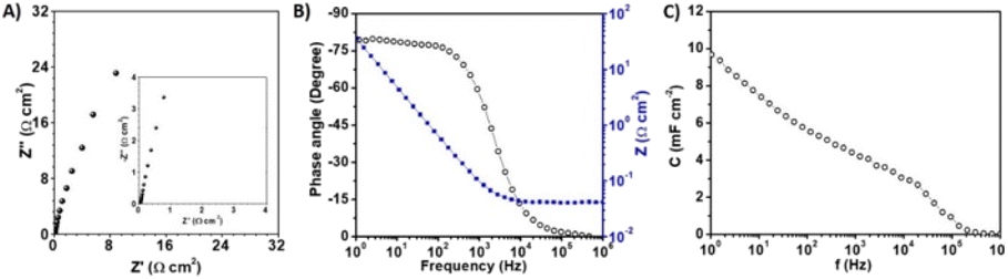
Electrochemical impedance spectroscopy (EIS) was conducted between 1 MHz and 1 Hz to further analyse the electrochemical behaviour of the FIB-fabricated NiRu/RuO2 nano-supercapacitor (Fig. 4). The Nyquist plot in Fig. 4A shows a near-perpendicular increase without a semicircular appearance, allowing the modelling of the device as a resistor and a capacitor connected in series. From the intercept with the x-axis, we can derive an electrolyte resistance of 0.057 Ω cm2 (inset in Fig. 4A), likely due to pronounced electrolyte ionic diffusion, which also likely accounts for the retention of the high areal capacitance at elevated scan rates.6,33
 | ||
| Fig. 4 Electrochemical impedance spectroscopy analysis. (A) Nyquist plot in a frequency range of 1 MHz–1 Hz. The inset shows a magnification of the high-frequency region. (B) Phase angle (Bode plot; black circles) and areal impedance (blue dots) as a function of the frequency (on a logarithmic scale). (C) The areal capacitance calculated from the imaginary component of the impedance as a function of frequency. | ||
The capacitive behaviour of the FIB-fabricated NiRu/RuO2 nano-supercapacitor was further investigated by calculating the phase angle as a function of frequency (Bode plot; Fig. 4B). As apparent in Fig. 4B, the phase angle at 120 Hz was −78°, reflecting an excellent capacitive behaviour in the conventional AC line-filtering working frequency. This value is better than that of many MSC systems,34–36 and only slightly lower than the −84° phase angle for a capacitor used in commercial line-filters.21,37
Fig. 4B also shows that a −45° phase angle, representing an equal capacitor and resistor behaviour, was attained at a frequency of ∼1500 Hz, accounting for device operation even at very high frequencies.30 The impedance as a function of the frequency (blue curve in Fig. 4B) yields an equivalent series resistance (ESR) of 0.047 Ω cm2 at an infinite frequency (determined via the intersection with the Y-axis). This low resistance value underscores the feasibility of high-power density applications of the NiRu/RuO2 nano-device. Fig. 4C depicts the areal capacitance, calculated from the imaginary component of the impedance, as a function of frequency.30 Notably, as apparent in Fig. 4C, the areal capacitance at 120 Hz is 5.6 mF cm−2, which is a significantly better value than many previous reports on planar MSCs.32,38,39 This result is likely due to the high surface area afforded by the NiRu/RuO2 nanostructures, attesting to the superior electrochemical properties of the device (see Fig. 3).
Fig. 5 depicts the galvanostatic charge–discharge (GCD) analysis designed to evaluate the capacitance and energy densities of the FIB-fabricated NiRu/RuO2 device. The galvanostatic charge–discharge (GCD) curves in a voltage window between 0 V and 1 V (Fig. 5A) reveal an excellent capacitive response reflected in the almost linear appearance and low voltage drop (0.018 V at 250 mA cm−2), representing a resistance of 0.072 Ω cm2. The areal capacitance as a function of current density, calculated from the GCD curves (Fig. 5B), reveals a high capacitance of 11 mF cm−2 at 250 mA cm−2 and almost 50% capacitance retention at 2000 mA cm−2, accounting for stable operation of the device even at high currents. The steeper curve in areal capacitance observed at low current densities (Fig. 5B) reflects the pseudocapacitive properties of the device, specifically allowing efficient redox reactions.40–42
 | ||
| Fig. 5 Electrochemical performance of the FIB-fabricated NiRu/RuO2 nano-supercapacitor. (A) GCD curves at a voltage window of 1.0 V and current densities of 250 mA cm−2, 500 mA cm−2, 750 mA cm−2, 1000 mA cm−2, and 2000 mA cm−2. (B) Areal capacitance as a function of current density, calculated from the GCD curves. (C) Ragone plot. Pertinent values of previously reported in-plane MSCs are cited. | ||
The Ragone plot in Fig. 5C presents the energy density vs. power density obtained for the FIB-fabricated NiRu/RuO2 nano-supercapacitor, in comparison with similar reported devices. Fig. 5C demonstrates that the NiRu/RuO2 nanodevice can operate at high power densities with a maximum energy density of 1.5 μW h cm−2 at a power density of 125 mW cm−2 and a maximum power density of 625 mW cm−2 with an energy density of 0.8 μW h cm−2. This result is remarkable for a supercapacitor exhibiting such small dimensionalities and is likely due to the extensive surface area of the NiRu/RuO2 nanostructures and high ion diffusion coefficient.23,32,36,43
Fig. 6 examines the FIB-fabricated NiRu/RuO2 nano-supercapacitor using polyvinyl alcohol (PVA)–KOH gel electrolyte, designed to evaluate practical applications in electronic circuits. Fig. 6A depicts CV curves recorded at scan rates between 0.01 and 400 V s−1. The corresponding calculated areal capacitance values are shown in Fig. 6B. The areal capacitance of 4.2 mF cm−2 at 10 V s−1 accounts for around 40% capacitance retention, likely accounting for the efficient interface between the electrode and the gel electrolyte. We further tested the operating voltage window of the PVA–KOH gel electrolyte through recording CV curves in different voltage windows (Fig. 6C). Notably, the CV curves in Fig. 6C confirm electrolyte stability and negligible electrolyte dissociation up to a potential window of 1.3 V. The GCD curves recorded at a voltage window of 1.3 V are depicted in Fig. 6D. The GCD analysis yields an aerial capacitance of 2.1 mF cm−2 at 400 mA cm−2, which is lower than that of the aqueous device but is sufficient for practical applications.
 | ||
| Fig. 6 Electrochemical characterization of the FIB-fabricated NiRu/RuO2 nano-supercapacitor with PVA–KOH gel electrolyte. (A) CV curves recorded at scan rates of 10 V s−1 (black), 50 V s−1 (red), 100 V s−1 (blue), 200 V s−1 (pink), and 400 V s−1 (green). (B) Areal capacitance vs. scan rate calculated from the CV curves. (C) CV curves recorded in increasing voltage windows, recorded at a scan rate of 10 V s−1. (D) GCD curves at a voltage window of 1.3 V and 400 mA cm−2, 600 mA cm−2, 800 mA cm−2, and 1000 mA cm−2 current densities. | ||
Fig. 7 presents the AC line-filtering performance of the FIB-fabricated NiRu/RuO2 nano-supercapacitor. Fig. 7A illustrates the circuit constructed for measuring the AC line filtering response, comprising a four-diode rectifier producing the AC half-wave signals (red waveform signal in Fig. 7B). The AC signal recorded after passage through the FIB-fabricated NiRu/RuO2 nano-supercapacitor, depicted in the bottom right in Fig. 7B, demonstrates the pronounced filtering effect of the device. Specifically, the ripple generated by the NiRu/RuO2 device (black output voltage) effectively traces the rectified signal recorded by a commercial ceramic aluminium oxide supercapacitor (blue output voltage). The calculated ripple factor of 0.5 obtained by the FIB-fabricated NiRu/RuO2 nano-supercapacitor represents an excellent line-filtering capacity.
 | ||
| Fig. 7 Alternating current (AC) line filtering by the FIB-fabricated NiRu/RuO2 nano-supercapacitor. (A) Schematic diagram of a low-pass filtering circuit integrated with the FIB-fabricated NiRu/RuO2 nano-supercapacitor. (B) Input and output voltage signals of the filtering circuit. AC input signal (pink), half wave filtered from the diode circuit (red), filtered signal from a commercial ceramic aluminum oxide supercapacitor (blue), and signal recorded via implementation of the NiRu/RuO2 device (black). | ||
Conclusions
We report a high-performance in-plane nano-supercapacitor comprising FIB-fabricated interdigitated electrodes coated with a NiRu/RuO2 layer. The novelty and uniqueness of our system lie both in the FIB fabrication producing 100 nm-wide trenches, and particularly the electrodeposition of a very thin (200 nm), high porosity NiRu/RuO2 electrochemically active layer, further enhanced by co-addition of KI to the electrolyte solution in the deposition stage and implemented for the first time in miniaturized inline micro-supercapacitors. The nanoscale dimensionalities reduce the electrolyte resistance of the device and produce excellent electrochemical parameters, generally superior to previously reported in-plane micro- and nano-supercapacitors. Electrochemical analyses of an aqueous NiRu/RuO2 device featured a phase angle of −78° at 120 Hz and ESR of 0.047 Ω cm2, reflecting excellent ion and electron transport properties essential for high frequencies and high current densities. The high areal capacitance of 5.28 mF cm−2, achieved at a current density of 2000 mA cm−2, further reflects excellent electrochemical properties. We also prepared a polymer-electrolyte device featuring good capacitive properties, underscoring the practical potential of the system. The FIB-fabricated NiRu/RuO2 nano-supercapacitor was successfully employed as an AC line filter, demonstrating, to the best of our knowledge, the smallest AC line filter reported. The new FIB-fabricated nano-supercapacitor design may open new application avenues, including miniaturized portable electronics, mobile power sources, micro- and nanorobotics, integrated circuits, and sensors.Experimental
Materials
RuCl3 hydrate (40–43% Ru) was purchased from STREM Chemicals and Na2SO4 (anhydrous 99%) and NiSO4·7H2O (99%) were purchased from Loba Chemie. Potassium hydroxide (KOH) was purchased from Merck and polyvinyl alcohol (PVA) was purchased from Sigma-Aldrich. All chemicals were used as received without further purification. The water used in the experiments was doubly purified by a Barnstead D7382 water purification system (Barnstead Thermolyne, Dubuque, IA), at 18.2 MΩ cm resistivity.NiRu electrochemical deposition and oxidation
Deposition and oxidation were conducted on an SP-150 Bio-Logic (Claix, France). A Ti/Ni layer (10 nm/200 nm) deposited on a Si wafer was prepared using e-beam assisted thermal evaporation. The electrochemical deposition of NiRu was carried out on the pre-deposited Ni film with dimensions of 100 μm by 100 μm prepared on a SiO2/silicon wafer. 1 M Na2SO4 deposition solution containing RuCl3 (0.003 M), NiSO4·7H2O (0.003 M) and KI (0.3 M) was used. The deposition was conducted using a 3-electrode configuration with the Ni on SiO2/Si as the working electrode, Pt wire as the counter electrode and Ag|AgCl (3 M KCl) as the reference electrode. Deposition was achieved using cyclic voltammetry (CV) cycles between 0 and −1.1 V vs. a reference electrode at a scan rate of 10 V s−1 for 2.5k cycles. Subsequent oxidation of the Ru to RuO2 was carried out by running 2.5k CV cycles at a scan rate of 10 V s−1 in a voltage window of 0–0.8 V using a 3-electrode configuration with NiRu as the working electrode, Pt wire as the counter electrode and Ag|AgCl (3 M KCl) as the reference electrode in 1 M Na2SO4 solution.Device fabrication using focused ion beam (FIB) milling
To fabricate the device, narrow trenches were fabricated on the electrode using FIB milling and the interdigitated device electrodes were fabricated as illustrated in Fig. 1B. Before the start of the FIB process, the deposited electrode was mounted on a stub holder grounded with copper tape and the sample was inserted into a dual beam FIB/SEM tool (Thermo Fisher, Helios G4 UC) to confirm surface uniformity. The sample was then placed at an angle of 52° with a low FIB current to align the ion beam without damaging the electrode surface. To fix a eucentric point on the electrode where FIB and SEM beams match, beams were focused on a point outside the device area. The sample was monitored for 1–1.5 h to observe any possible appearance of surface charging of the electrode before application of FIB to achieve precise nanopatterning. Subsequently, Ga+ ions were accelerated in vacuo at 30 kV resulting in the ejection of sputtered particles. Using FIB patterning, we sculpted 10 “nano-fingers” in each electrode, exhibiting widths of 5 μm and separated by 100 ± 25 nm created with an optimized high energy current of 0.79 nA with an 80 nm spot size. The FIB-constructed separation trench depth was 600 nm to prevent electrical shorting due to contact between adjacent fingers. Square holes were further created at the trench corners, designed to maintain sufficient separation between the finger edges.Gel electrolyte preparation
The PVA/KOH gel electrolyte was prepared by taking 1 g (56.1056 g mol−1) of KOH and 1 g (44.05 g mol−1) of PVA and dissolving them homogeneously in 20 ml of distilled water at 80 °C with continuous magnetic stirring for ∼10 h. After successful formation of the homogenized solution, it was poured into a single vial and mixed uniformly overnight.Characterization
X-ray photoelectron spectroscopy (XPS) analysis was carried out using a Thermo Fisher ESCALAB 250 instrument (England) with a basic pressure of 2 × 10⁻⁹ mbar using monochromatic Al Kα 1486.6 eV X-rays, using a beam size of 500 μm. The core level binding energies of the Ru 3d peaks were normalized by setting the binding energy for the C 1s at 284.8 eV. High resolution transmission electron microscopy (HRTEM) images were recorded on a 200 kV JEOL JEM-2100F (Tokyo, Japan). Scanning electron microscopy (SEM) images were recorded on a Verios 460 L FEI (Czech Republic). Scanning transmission electron microscopy (STEM) images were recorded on a Helios G4 UC instrument and electron dispersion spectroscopy (EDS) maps were measured on the same instrument with a silicon drift X-ray detector (Brooker Xflash60) for 5 min at 15 kV and current of 1.6 nA. Lamellas for cross section TEM imaging were fabricated using a Helios G4 UC dual beam FIB/SEM (Thermo Fisher Scientific).Lamella preparation for HRTEM
Lamellas for cross section for TEM imaging were fabricated using a Helios G4 UC dual beam FIB (Thermo Fisher Scientific). The sample was covered with 1.0 μm of Pt using electron deposition followed by another 0.5 μm carbon deposition. A Ga+ ion beam was employed to mill the cross section of the protective area and an Easylift (Thermo Fisher Scientific) micro-manipulator was used to lift the lamellas and place them on a TEM grid. The lamellas were subsequently cleaned with a 30 kV Ga ion beam from both sides and the thickness was reduced to ∼150 nm and ∼50 nm in successive steps with a reduced probe potential of 5 kV.Electrochemical measurements
The electrochemical testing of the device was conducted on an SP-150 Bio-Logic (Claix, France). Cyclic voltammetry (CV) was conducted in voltage ranges between 0 and 1 V (aqueous device) and 0 and 1.4 V (gel electrolyte). Galvanostatic charge/discharge measurements were conducted at current densities in the range of 250–2000 mA cm−2 in a voltage window of 1.0 V. Electrochemical impedance measurements were conducted between 1 Hz and 100 kHz with a sinusoidal amplitude of 10 mV. Cycling stability measurements were conducted at a scan rate of 10 V s−1 in a voltage window of 0–1 V for 10k cycles.Data availability
The data supporting this article have been included as part of the ESI.†Author contributions
Conceptualization: S. Biswas, A. Morag, and R. Jelinek; data curation: S. Biswas, N. Maman, and N. Shauloff; formal analysis: S. Biswas and R. Jelinek; funding acquisition: R. Jelinek; methodology: S. Biswas, A. Morag, and R. Jelinek; supervision: R. Jelinek; visualization: S. Biswas and A. Morag; writing – original draft: S. Biswas; writing – review & editing: A. Morag, N. Maman, and R. Jelinek.Conflicts of interest
There are no conflicts to declare.Acknowledgements
The authors thank Dr Vladimir Ezersky for help with the HRTEM experiments, and Dr Natalya Froumin for assistance with the XPS measurements. We are grateful to the Ministry of Energy Research, Israel for the research supporting grant with award number 1096/23. The authors also thank David Rahmilov and Ahron Rivni for providing the instrumentation in AC filter measurements.References
- S. Rani, N. Kumar and Y. Sharma, J. Phys.: Energy, 2021, 3(3), 032017 CAS.
- L. M. M. Ferro, L. Merces, H. Tang, D. D. Karnaushenko, D. Karnaushenko, O. G. Schmidt and M. Zhu, Adv. Mater. Technol., 2023, 8(15), 2300053 CrossRef CAS.
- Q. Muhammad Saqib, A. Mannan, M. Noman, M. Y. Chougale, C. S. Patil, Y. Ko, J. Kim, S. R. Patil, M. Yousuf, R. Ali Shaukat, Y. Pyo Jeon, D. Dubal and J. Bae, Chem. Eng. J., 2024, 490, 151857 CrossRef CAS.
- D. Pech, M. Brunet, H. Durou, P. Huang, V. Mochalin, Y. Gogotsi, P. L. Taberna and P. Simon, Nat. Nanotechnol., 2010, 5, 651–654 CrossRef CAS.
- Z. S. Wu, K. Parvez, A. Winter, H. Vieker, X. Liu, S. Han, A. Turchanin, X. Feng and K. Mullen, Adv. Mater., 2014, 26, 4552–4558 CrossRef CAS.
- T. M. Dinh, K. Armstrong, D. Guay and D. Pech, J. Mater. Chem. A, 2014, 2, 7170–7174 RSC.
- B. Dousti, S. Babu, N. Geramifard, M. Y. Choi, J. B. Lee, S. F. Cogan and G. S. Lee, J. Power Sources, 2022, 520, 230779 CrossRef CAS.
- J. Du, Y. Zhao, Z. Zhang, X. Mu, X. Jiang, B. Huang, Y. Zhang, S. Zhang, Z. Zhang and E. Xie, J. Mater. Chem. A, 2019, 7, 6220–6227 RSC.
- D. Qi, Y. Liu, Z. Liu, L. Zhang and X. Chen, Adv. Mater., 2017, 29(46), 1703852 CrossRef.
- C. J. Zhang, L. McKeon, M. P. Kremer, S. H. Park, O. Ronan, A. Seral-Ascaso, S. Barwich, C. O. Coileain, N. McEvoy, H. C. Nerl, B. Anasori, J. N. Coleman, Y. Gogotsi and V. Nicolosi, Nat. Commun., 2019, 10, 1795 CrossRef.
- H. Liu, Z. Sun, Y. Chen, W. Zhang, X. Chen and C. P. Wong, ACS Nano, 2022, 16, 10088–10129 CrossRef CAS PubMed.
- Z.-S. Wu, K. Parvez, X. Feng and K. Müllen, J. Mater. Chem. A, 2014, 2, 8288 RSC.
- N. P. Maxime Darnon, in Plasma Etching Processes for CMOS Devices Realization, ed. N. Posseme, 2017, pp. 95–118, DOI:10.1016/B978-1-78548-096-6.50004-3.
- D. J. Ehrlich and J. Y. Tsao, J. Vac. Sci. Technol., B: Microelectron. Process. Phenom., 1983, 1, 969–984 CrossRef CAS.
- R. M. M. Hasan and X. Luo, Nanomanuf. Metrol., 2018, 1, 67–81 CrossRef.
- X. Feng, X. Shi, J. Ning, D. Wang, J. Zhang, Y. Hao and Z.-S. Wu, eScience, 2021, 1, 124–140 CrossRef.
- C. Chen, J. Cao, X. Wang, Q. Lu, M. Han, Q. Wang, H. Dai, Z. Niu, J. Chen and S. Xie, Nano Energy, 2017, 42, 187–194 CrossRef CAS.
- J. Wang, X. Wang, S. W. Lee and Q. Zhang, ACS Appl. Mater. Interfaces, 2019, 11, 40481–40489 CrossRef CAS.
- Y. Yoo, S. Kim, B. Kim and W. Kim, J. Mater. Chem. A, 2015, 3, 11801–11806 RSC.
- Y. Yoo, M.-S. Kim, J.-K. Kim, Y. S. Kim and W. Kim, J. Mater. Chem. A, 2016, 4, 5062–5068 RSC.
- H. Tang, Y. Tian, Z. Wu, Y. Zeng, Y. Wang, Y. Hou, Z. Ye and J. Lu, Energy Environ. Mater., 2022, 5, 1060–1083 CrossRef CAS.
- Q. Jiang, N. Kurra, K. Maleski, Y. J. Lei, H. F. Liang, Y. Z. Zhang, Y. Gogotsi and H. N. Alshareef, Adv. Energy Mater., 2019, 9(26), 1901061 CrossRef.
- P. Zhuang, Y. Sun, L. Li, M. O. L. Chee, P. Dong, L. Pei, H. Chu, Z. Sun, J. Shen, M. Ye and P. M. Ajayan, Adv. Mater., 2020, 32, e1908072 CrossRef PubMed.
- A. Ferris, B. Reig, A. Eddarir, J.-F. Pierson, S. Garbarino, D. Guay and D. Pech, ACS Energy Lett., 2017, 2, 1734–1739 CrossRef CAS.
- D. E. Lobo, P. C. Banerjee, C. D. Easton and M. Majumder, Adv. Energy Mater., 2015, 5(19), 1500665 CrossRef.
- E. Kim, B.-J. Lee, K. Maleski, Y. Chae, Y. Lee, Y. Gogotsi and C. W. Ahn, Nano Energy, 2021, 81, 105616 CrossRef CAS.
- F. S. Jamaludin, M. F. Mohd Sabri and S. M. Said, Microsyst. Technol., 2013, 19, 1873–1888 CrossRef.
- T. Sardhara, A. Shkurmanov, Y. Li, S. Shi, C. J. Cyron, R. C. Aydin and M. Ritter, Ultramicroscopy, 2024, 256, 113878 CrossRef CAS.
- M. Kroupa, G. J. Offer and J. Kosek, J. Electrochem. Soc., 2016, 163, A2475–A2487 CrossRef CAS.
- A. Morag, N. Shauloff, N. Maman, N. Froumin, V. Ezersky and R. Jelinek, Batteries Supercaps, 2020, 3, 792 CrossRef CAS.
- J. Goodenough, Prog. Solid State Chem., 1971, 5, 145–399 CrossRef CAS.
- J. Lin, C. Zhang, Z. Yan, Y. Zhu, Z. Peng, R. H. Hauge, D. Natelson and J. M. Tour, Nano Lett., 2013, 13, 72–78 CrossRef CAS PubMed.
- Z. S. Wu, Z. Liu, K. Parvez, X. Feng and K. Mullen, Adv. Mater., 2015, 27, 3669–3675 CrossRef CAS.
- L. Yao, J. Liu, N. Eedugurala, P. Mahalingavelar, D. J. Adams, K. Wang, K. S. Mayer, J. D. Azoulay and T. N. Ng, Cell Rep. Phys. Sci., 2022, 3(6), 101446 Search PubMed.
- N. Ji, J. Park and W. Kim, ACS Omega, 2019, 4, 18900–18907 CrossRef CAS.
- G. S. Gund, J. H. Park, R. Harpalsinh, M. Kota, J. H. Shin, T.-I. Kim, Y. Gogotsi and H. S. Park, Joule, 2019, 3, 164–176 CrossRef CAS.
- S. Zhang, B. Li, C. Cui, W. Qian and Y. Jin, Batteries Supercaps, 2023, 6(3), e202200476 CrossRef CAS.
- G. Ren, S. Li, Z.-X. Fan, M. N. F. Hoque and Z. Fan, J. Power Sources, 2016, 325, 152–160 CrossRef CAS.
- S. Xu, W. Liu, B. Hu and X. Wang, Nano Energy, 2019, 58, 803–810 CrossRef CAS.
- F. Qui, R. Zhao, M. Yi, P. Qi, C. Chai, H. Ying and J. Hao, Chem. Eng. J., 2021, 413, 131107 Search PubMed.
- A. Peksoz, R. Mohammadigharehbagh, K. Erturk, S. K. Akay and S. Sarsici, J. Mater. Sci.: Mater. Electron., 2022, 33, 20756–20768 CrossRef CAS.
- P. Dubey, V. Shrivastav, B. Gupta, M. Hołdyński, W. Nogala and S. Sundriyal, Diamond Relat. Mater., 2022, 130, 109529 CrossRef CAS.
- Y. Yusran, H. Li, X. Guan, D. Li, L. Tang, M. Xue, Z. Zhuang, Y. Yan, V. Valtchev, S. Qiu and Q. Fang, Adv. Mater., 2020, 32, e1907289 CrossRef.
Footnote |
| † Electronic supplementary information (ESI) available. See DOI: https://doi.org/10.1039/d4ta03734k |
| This journal is © The Royal Society of Chemistry 2024 |