
Eye-wearable Ti3C2Tx MXene-based micro-supercapacitor as a power unit for intraocular pressure applications†
Weijia
Liu
a,
Zhijian
Du
a,
Zhongyi
Duan
a,
Haiqing
Liu
a,
La
Li
 *a,
Kai
Jiang
*b,
Di
Chen
a and
Guozhen
Shen
*a
*a,
Kai
Jiang
*b,
Di
Chen
a and
Guozhen
Shen
*a
aSchool of Integrated Circuits and Electronics, Beijing Institute of Technology, Beijing 100081, China. E-mail: lali@bit.edu.cn; gzshen@bit.edu.cn
bFaculty of Hepato-Pancreato-Biliary Surgery, Chinese PLA General Hospital, Institute of Hepatobiliary Surgery of Chinese PLA, Key Laboratory of Digital Hepatobiliary Surgery, Beijing, 100853 P. R. China. E-mail: jiangk301@126.com
First published on 25th May 2024
Abstract
Ocular devices worn on human eyeballs with hemispherical appearance and intelligent functions are expected to perform continuous and nondestructive oculopathy disease management because human eyes contain abundant physiological and biochemical information. However, fabricating and integrating different devices on the hemispherical surface with varying curvature remains a challenge. Herein, we report a Ti3C2Tx MXene-based hemispherical integrated system that connects a micro-supercapacitor (MSC) and strain sensors to form self-powered devices for intraocular pressure monitoring. The use of the same Ti3C2Tx MXene material as the electrode material of MSC and piezoresistive films of the strain sensors greatly reduces the complexity of the manufacturing process. The high specific capacitance (32 mF cm−2) at a scan rate of 5 mV s−1 and energy density (10 mW h cm−2) of the Ti3C2Tx MXene-based MSC enable stable output voltage to drive the strain sensor. Meanwhile, the Ti3C2Tx strain sensor provides a superior sensitivity of 0.014 mmHg−1 and a wide sensing range varying from 0 to 50 mmHg, which can realize continuous IOP monitoring. Furthermore, the self-powered hemispherical integrated device provides rapid and stable response to different IOP, holding great promise for oculopathy diagnosis and treatment.
Introduction
Human eyes are the most complicated and important organs of the human body; more than 80% of the information received by our brain comes from our eyes.1–3 Additionally, eyes contain abundant physiological and biochemical information that be used in oculopathy diagnosis and treatment.4–6 Therefore, wearing ophthalmic devices for continuous and real-time eye monitoring has great implications for understanding our level of health and reducing morbidity.7 Recent advances in wearable technologies have brought changes in how these ophthalmic illnesses are diagnosed and managed.8 Unlike our skin with bent or stretchable properties, ocular devices worn on human eyeballs require to be designed with a hemispherical structure to match the demands of the sphere-shaped eyeballs.9,10 This poses huge challenges for wearable ocular devices. Moreover, when wearing ocular devices on the eyeballs built with safety and comfort in mind, the wearable devices must be biocompatible and soft.11,12Intraocular pressure (IOP), as one of the crucial physiological signals contained in eyes, which reflects the state of aqueous humor circulation, can provide qualitative diagnostic bases of eye diseases to guide individual therapy.13 Among them, glaucoma shows that IOP increases intermittently or continuously, threatening the optic nerve and visual function, which has no obvious symptoms in the early stage.14 Currently, IOP is the only controllable and measurable factor in the treatment of glaucoma.15,16 Therefore, fabricating wearable ocular devices for continuous IOP monitoring could help prevent glaucoma through early detection and avoid vision loss.17,18 To meet the requirement of continuous IOP monitoring, the wearable ocular devices must at least comprise two components, namely, energy supply and IOP sensor.19 Recently, Park et al. reported on a hemispherical integrated sensing system to detect the IOP change, where the rigid chip is introduced in the integrated system to power the IOP strain sensor.11 Although they achieved real-time IOP monitoring, the introduction of a rigid chip brings foreign body sensation.
Micro-supercapacitors (MSCs), with small size, high security, long cycle stability, and suitable energy density, have been demonstrated as a promising energy supply for wearable sensors. The problems for driving in-eye intraocular pressure monitoring devices that need to be overcome mainly focus on the fabrication of hemispherical structures and the in-eye safety.20,21 In a previous work, we reported a flexible Zn-ion hybrid MSCs based on a Ti3C2Tx–DMSO cathode and a redox-active electrolyte, whose high rate performance and good cycling stability can drive the integrated pressure sensor to undergo a fast and stable response, but its planar structural design and the additive-assisted Zn(CF3SO3)2 electrolyte limit the eye-wear of the integrated system.22
In this work, we proposed a facile laser scribing-assisted spray coating method to prepare Ti3C2Tx MXene-based MSC and strain sensor on the hemispherical deformable substrate and then fabricated the hemispherical integrated devices via water transfer technology. The P(VDF-TrFE) substrate achieves stress concentration through a thickness partitioning strategy, increasing the thickness of the substrate in the capacitor region to improve the stability of the energy supply while decreasing the thickness of the strain sensor substrate to improve the sensitivity of intraocular pressure (IOP) monitoring, which ultimately achieves the optimal system performance output. The as-prepared Ti3C2Tx MXene-based MSC exhibits a high specific capacitance of 32 mF cm−2 at a scan rate of 5 mV s−1 and energy density of 10 mW h cm−2 at a power density of 0.9 mW cm−2, offering a stable output voltage for the strain sensor. The Ti3C2Tx strain sensor shows a high sensitivity of 0.014 mmHg−1, a wide range ranging from 0 to 50 mmHg, superior linearity, and excellent stability. By connecting the Ti3C2Tx MXene-based MSC with the strain sensor, the hemispherical integrated devices show an independent and stable response to different IOP, demonstrating the possibility of the self-powered hemispherical integrated wearable ocular devices, which may take important roles in future health monitoring and treatment devices.
Experimental
Materials
The two-dimensional (2D) Ti3C2Tx MXene nanosheets were synthesized using a mixed acid (hydrofluoric acid and hydrochloric acid, Tianjin Fuyu Fine Chemical Co., Ltd) etching process. Briefly, 13.5 mL of hydrochloric acid (HF), 3 mL of hydrofluoric acid (HCl), and 1.5 g of MAX Phase (Ti3AlC2, Carbon-Ukraine) were slowly added sequentially to 13.5 mL of DI-water and magnetically stirred at 40 °C for 24 h. The etched precipitate was then rinsed repeatedly with DI-water at 3500 rpm until the supernatant reached a neutral pH to obtain the multilayer Ti3C2Tx MXene. Subsequently, the multilayer Ti3C2Tx MXene was dissolved in 30 mL of DI-water, and 3.5 g lithium chloride (LiCl, Innochem) was added for 8 h in this solution stirred at high speed. After completing the insertion and washing off the LiCl from the solution, the precipitate was washed with DI-water several times at 4000 rpm, assisted by handshaking, and the upper black colloidal solution after each centrifugation was collected to obtain a monolayer 2D Ti3C2Tx MXene.Fabrication of hemispherical integrated device
The prepared 2D Ti3C2Tx MXene was first dried in a vacuum environment at 60 °C for 12 h and then dissolved into 13.3 mL N,N-dimethylformamide (DMF, Innochem) to obtain the Ti3C2Tx–DMF solution with a concentration of 15 mg mL−1, followed by the addition of 2 g P(VDF-TrFE) (VDF![[thin space (1/6-em)]](https://www.rsc.org/images/entities/char_2009.gif) :TrFE = 80%:20%, France PIEZOTECH) magnetically stirred until the formation of a homogeneous P(VDF-TrFE)@Ti3C2Tx MXene gelatinous solution for later use.
:TrFE = 80%:20%, France PIEZOTECH) magnetically stirred until the formation of a homogeneous P(VDF-TrFE)@Ti3C2Tx MXene gelatinous solution for later use.
Firstly, the glass plate was ultrasonically cleaned with ethanol and water, respectively, and then spin-coated with the P(VDF-TrFE)@Ti3C2Tx MXene colloidal solution at 500 rpm for 10 s, which was further heated at 35 °C for 20 min. After the solvent had been evaporated, the film was etched with a laser (MC-UV-20W, the laser speed, current, frequency, and the pulse width were 500 mm s−1, 1 A, 150 kHz, and 1 μs, respectively), following the pre-designed pattern of the capacitor and the sensor, and then the sensor part substrate was replaced with a thinner film (1500 rpm, 10 s) and soldered to the capacitor substrate with the P(VDF-TrFE)@Ti3C2Tx MXene solution. Subsequently, the patterned film underwent plasma treatment and was sprayed with 2 mL monolayer Ti3C2Tx MXene solution at a concentration of 2 mg mL−1 at 60 °C. The film outside of the electrode pattern was peeled-off and spin-coated with 5% polyethylene oxide (PEO, MW = 100000, Innochem) solution at 700 rpm, then dried at 60 °C for 0.5 h. Thereafter, the PEO film together with the electrodes was removed from the glass plate and placed parallel to it between the tap and the hemispherical mold covered with polydimethylsiloxane (PDMS, main agent:curing agent = 90%:10%) film, while the electrodes were transferred intact to the PDMS hemispherical film under the action of water rinsing in the process of film dissolution. In the next step, a layer of NaCl (sodium chloride, 0.3 M, Innochem)/PVA (polyvinyl alcohol-1799, 10 wt%, Innochem) gel electrolyte was uniformly applied on top of the electrodes of the MSC, and a layer of PDMS solution was subsequently dripped onto the top of the electrolyte after the surface was slightly solidified. Finally, the self-driven IOP smart contact lens was obtained by removing the entire device from the mold after the encapsulated PDMS was completely dry.
Characterization and testing
The morphological characteristics of multilayer and monolayer Ti3C2Tx MXene as well as the screenshot of the substrate and electrode materials of the MSC were observed by field emission scanning electron microscopy (FESEM, JOEL JSM-7500F). The size and elemental composition of the monolayer Ti3C2Tx MXene nanosheets were analyzed using field emission transmission electron microscopy (FETEM, FEI Tecnai G2 F30).The thickness of the individual monolayer Ti3C2Tx MXene nanosheet was measured by atomic force microscopy (AFM, Bruker Dension Icon). The thickness of the Ti3C2Tx MXene functional electrodes as well as the films formed by spin coating at 500 rpm, 750 rpm, 1000 rpm, and 1500 rpm, respectively, were measured by the step profiler (Dektak XT, Bruker). The photographs of the MSC and IOP sensor were taken with an optical microscope (ZEISS Imager M1m), and the widths of the MSC channel and sensor electrode were measured.
The stress–strain curves and sensitivity of the Ti3C2Tx MXene electrodes based on the P(VDF-TrFE)@Ti3C2Tx MXene substrates of different widths (500 μm, 1000 μm, 1500 μm and 2000 μm) and thicknesses (500 rpm, 750 rpm, 1000 rpm and 1500 rpm) encapsulated by PDMS films were tested under different compressive forces using a tensile machine (Dektak XT, Bruker). The electrochemical performance of the MSCs was tested using an electrochemical workstation (CHI 760D), and the performance of the IOP sensors was tested using an original meter.
Results and discussion
IOP changes have been proven to transmit many significant physiological and neurological signals, such as early eye diseases (glaucoma, etc.), and psychological conditions (mania, etc.).23,24 Therefore, strain sensors based on resistance changes are expected to be adopted in noninvasive hemispherical integrated device for real-time IOP monitoring. However, the power supply is a necessary problem that needs to be solved in the direction of multi-functional and multi-ecological ocular devices. The hemispherical integrated device was prepared by integrating a resistive IOP sensor and the hydrogel-based MSCs module to provide accurate, real-time IOP data while delivering the necessary power to the sensor. As shown in Fig. 1a, the schematic shows the IOP sensor and Ti3C2Tx-MSCs, two modules forming the device. Its vertical structure can be divided into five layers, consisting of the upper and lower PDMS packaging layers, a PVDF substrate, a Ti3C2Tx MXene conductive layer, and a NaCl@PVA solid electrolyte. According to the microscope photography (Fig. 1b and c), the channel width between the two electrodes from the Ti3C2Tx-MSCs module is 400 μm; in the IOP sensor module, the width of the sensing line is 500 μm. P(VDF-TrFE) casting membrane was used as the substrate of the whole device. The sprayed Ti3C2Tx MXene membrane was utilized as the conductive layer with a thickness of 5.04 μm (Fig. 1d). It is worth mentioning that the Ti3C2Tx MXene membrane obtained by the spraying process is denser. The conductive medium Ti3C2Tx MXene was prepared by the selective etching of Ti3AlC2 MAX and mechanical stratification. As shown in Fig. 1e, the etched Ti3C2Tx presents an accordion-like shape, and a large number of two-dimensional mono or few layers of Ti3C2Tx MXene can be seen by SEM and TEM after layering (Fig. S1–S3†).25,26 The AFM image in Fig. 1f shows that its thickness is about 1.02 nm. The Raman spectrum of Fig. S4† is divided into three regions: the flake region (202 cm−1), which corresponds to a group vibration of carbon, two titanium layers, and surface groups, the Tx region (230–470 cm−1), which represents vibrations of the surface groups, and the carbon region (580–730 cm−1), where both in-plane and out-of-plane vibrations of carbon atoms are located.22 The morphology of the whole device is shown in Fig. 1g. The IOP sensor and Ti3C2Tx-MSCs modules were placed in the peripheral field of the visual field and the area of the IOP energy supply. There are no electronic components in the field of view; thus, testers will not be disturbed after wearing the hemispherical integrated device.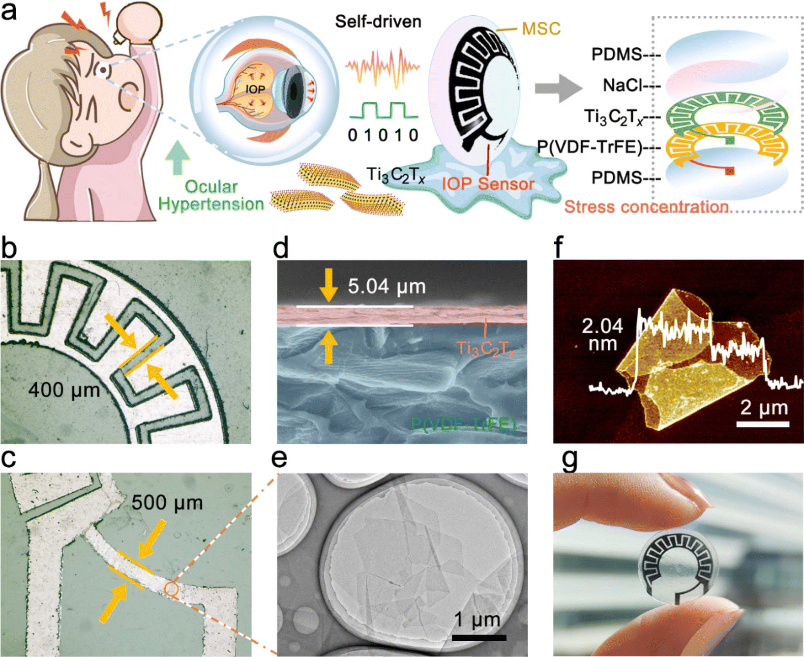 | ||
| Fig. 1 (a) Schematic illustration and structure of the hemispherical integrated device. (b) Width of the channel between the interdigital electrodes of Ti3C2Tx-MSCs module in the device. (c) Width of the IOP sensor module in the device. (d) SEM image at the cross section of the MSC device. (e) TEM image of Ti3C2Tx MXene. (f) AFM image of Ti3C2Tx MXene. (g) Optical photograph of the hemispherical integrated device. | ||
The hemispherical integrated device was fabricated via laser scribing-assisted spray-coating technology, electrode transfer, and stress-concentration design strategies incorporating the substrates (Fig. 2a, detailed steps are shown in the Experimental section). First, the P(VDF-TrFE)@Ti3C2Tx membrane was divided into a substrate area and a cover area by laser scribing, which ensured high-precision electrode patterning while avoiding tensile stress on the film, thus ensuring electrode conductivity. The spraying process leads to the introduction of more defects into the functional electrode based on ensuring the good electrical conductivity of the two-dimensional material, which is favorable to the embedding and release of ions in the electrolyte, and at the same time, the introduction of defects weakened the van der Waals force between the nanosheets to a certain extent, and the slipping was more obvious under the same stress, which then improved the sensitivity of the IOP sensor extremely well. More importantly, the electrode was peeled off with a water-soluble film and adapted to attach to the hemispherical substrate by the force of water, thereby avoiding the damage to the electrodes prevalent in conventional thermal pressing techniques.27 Finally, an eye-compatible NaCl/PVA-gel electrolyte and PDMS encapsulation were applied dropwise to the electrodes to prevent eye damage from the leakage of conventional electrolytes.
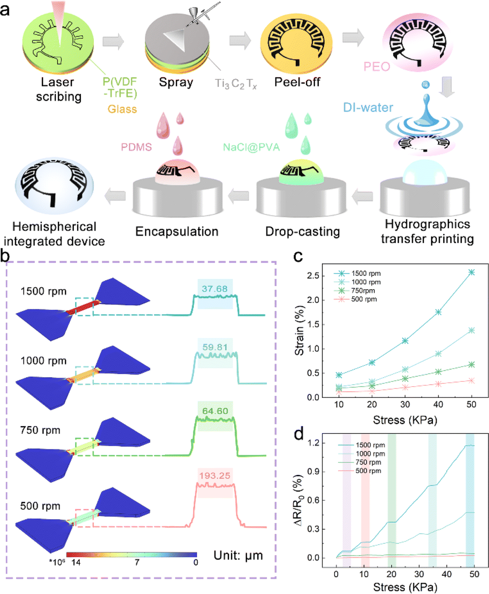 | ||
| Fig. 2 (a) Schematic illustration showing the design and fabrication process of the hemispherical integrated device. (b) FEA simulations for P(VDF-TrFE) membranes with different thicknesses under 50 kPa tensile stresses and corresponding thicknesses measured using a step meter. (c) Stress–strain curves of 200 μm wide P(VDF-TrFE) membranes prepared with different thicknesses. (d) ΔR/R0 values of the sensor with different thicknesses of the P(VDF-TrFE) substrates following different stresses. | ||
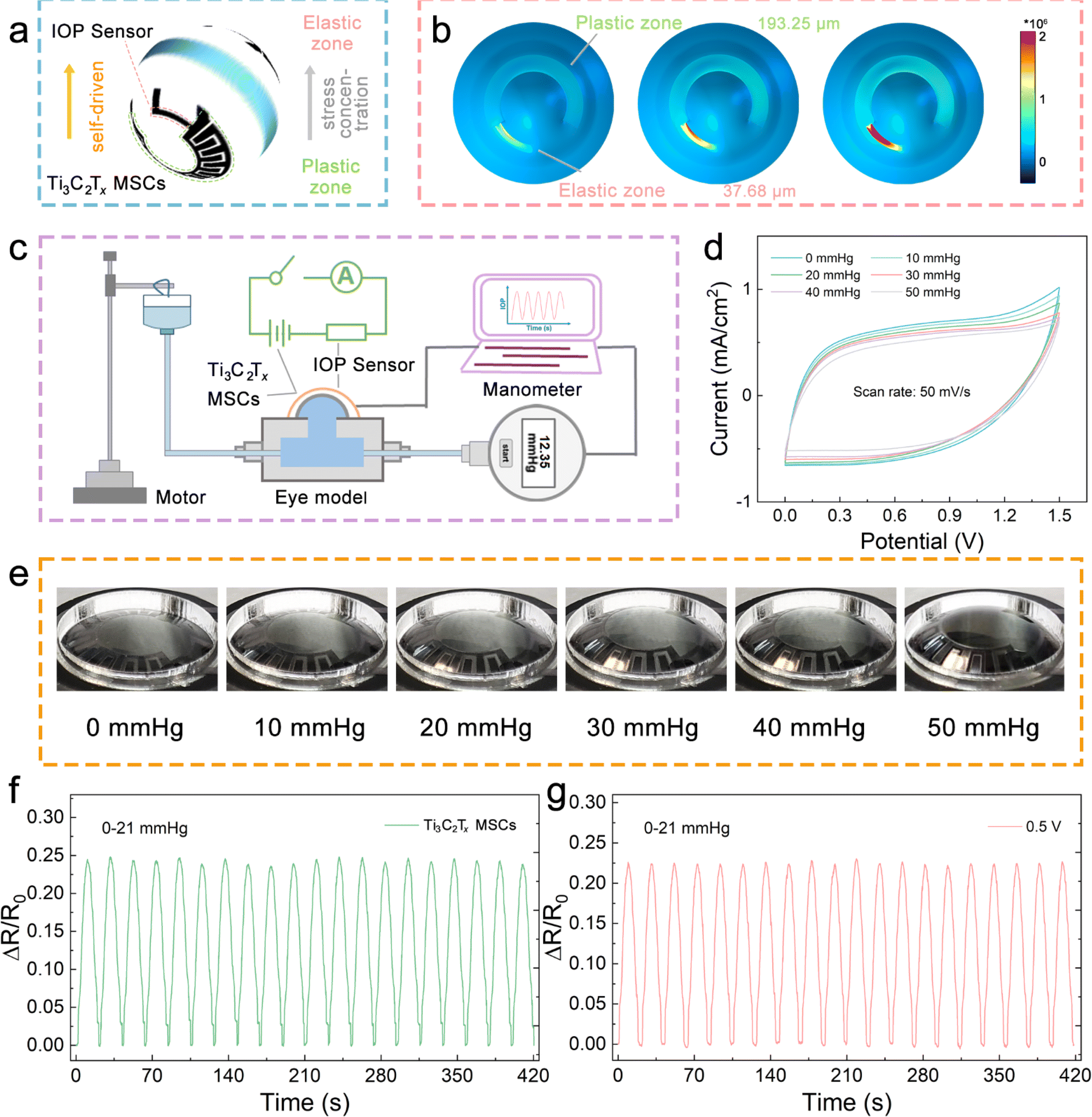
The stress-concentration is strongly influenced by the substrate closely attached to the conductive layer.28,29 The soft substrate can induce and promote the conductive layer to change the directional movement efficiency of the electrons, which comes from the substrate with low modulus to maximize the absorption and transfer of stress. The copolymer of PVDF, P(VDF-TrFE), has a reduced crystallinity; thus, its cast membrane exhibits excellent mechanical properties.30 Therefore, as shown in Fig. 2b and S5,† the FEA simulations of the P(VDF-TrFE) membranes with different thicknesses under fixed stress fields show that thinner membranes exhibit more prominent stress absorption. It is worth mentioning that the thickness of the P(VDF-TrFE) substrate is achieved by controlling the spin-coating rate, which was 193.25 μm for the 500 rpm spin-coated film and 37.68 μm for the 1500 rpm spin-coated film. At the same time, the stress–strain curves of a series of membranes were recorded and are shown in Fig. 2c. The results further suggest that the thinner membranes have more considerable displacement changes under the same stress stretching. In addition, the sensitivity–stress curves of the membranes demonstrate that thinner membranes also have the potential as substrate materials for tensile sensors because of their outstanding flexibility (Fig. 2d).
To achieve reliable power use without safety concerns in hemispherical integrated devices, water-based MSCs are the power source of choice. The design of Na+ ions as a carrier to carry and transport electrical charges is because Na+ ions are generally present in tears at a higher concentration than in body fluids; thus, a suitable concentration of Na+ ions is required as the electrolyte will not cause adverse effects on the eyeball (Fig. 3a).31 The electrochemical performances of the Ti3C2Tx MXene electrodes were evaluated with a three-electrode system in 0.3 M NaCl electrolyte. The approximate rectangular CV curves at 5–100 mV s−1 and the triangular galvanostatic charge/discharge (GCD) curves at 0.4–1.5 mA cm−2 are displayed in Fig. S6a and b,† implying that the Ti3C2Tx MXene electrodes store more charge and have excellent electrochemical performance. As shown in Fig. S6c,† the Ti3C2Tx MXene exhibits a small semicircle in the high-frequency region and a large slope in the low-frequency region in the electrochemical impedance spectroscopy (EIS) result, indicating its small electron transfer resistance and faster ion-diffusion rate, presumably a result of the large layer spacing between the nanosheets that provide fast and direct ion transportation pathways. The highest area capacitance was calculated from the CV curve to be 149.3 mF cm−2 (5 mV s−1), and the capacity retention was still 62.3% at a scan rate of 100 mV s−1 (Fig. S6d†).
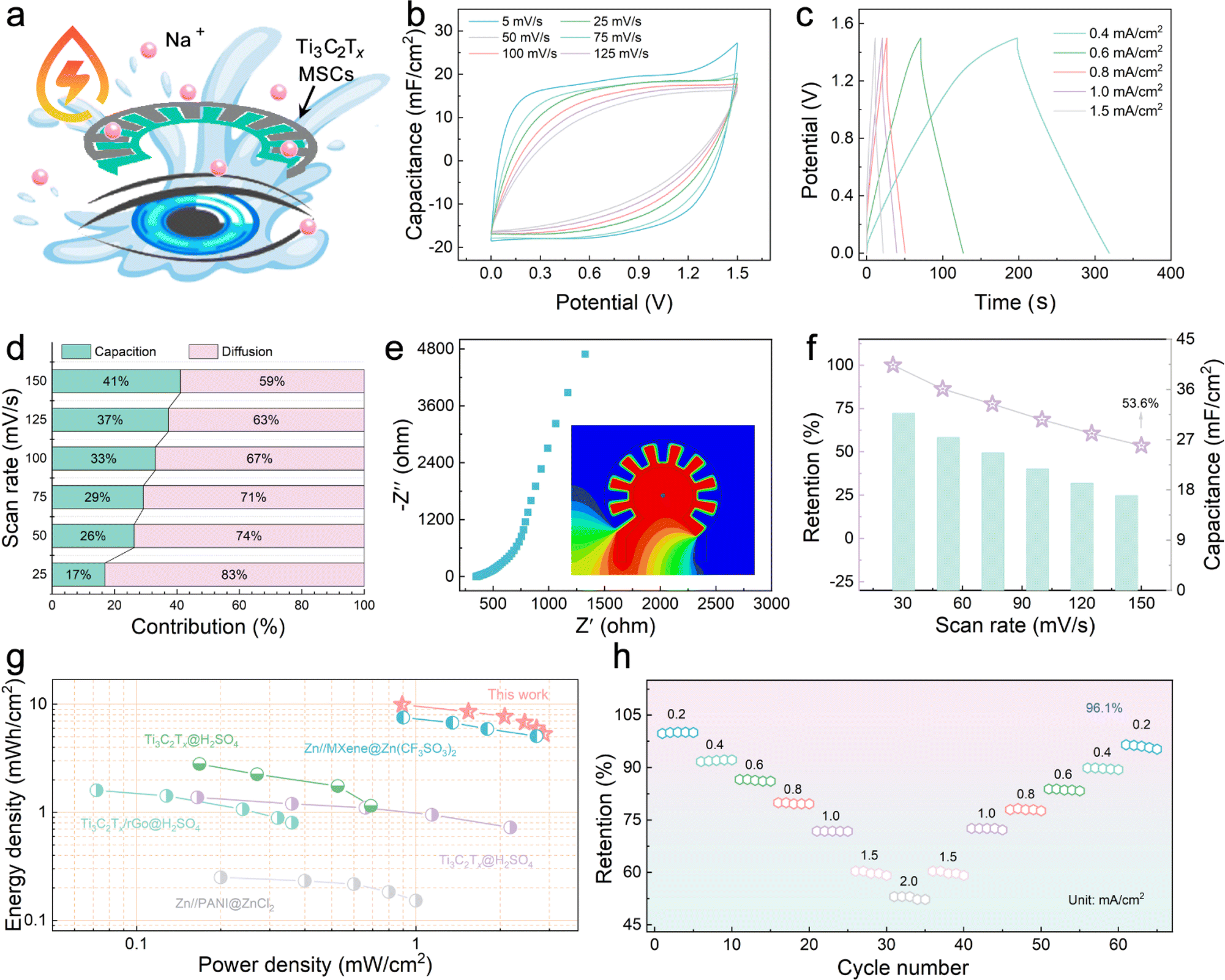 | ||
| Fig. 3 (a) Schematic of the Ti3C2Tx-MSCs. (b) CV curves at different scan rates. (c) GCD curves at different current densities. (d) Capacitive and diffusion contribution ratio of Ti3C2Tx-MSCs at different scan rates. (e) EIS plots and simulated energy distribution of Ti3C2Tx-MSCs. (f) Variation of areal capacitance and capacitance retention with various scan rates. (g) Ragone plot of areal energy density vs. power density for Ti3C2Tx-MSCs in comparison with the reported MSCs. (h) The rate properties of the Ti3C2Tx-MSCs at different current densities. | ||
NaCl was dissolved in PVA solution to obtain a solid electrolyte, and Ti3C2Tx MXene with abundant charge adsorption sites was used as the electrode to prepare a patterned Ti3C2Tx-MSCs that complied with the requirements of the viewing field. Fig. S7† shows that the voltage window of the Ti3C2Tx-MSCs can reach an attractive 1.4 V without decomposition of the medium. Fig. 3b and S8† display the CV curves of fabricated Ti3C2Tx-MSCs at scan rates ranging from 5 to 125 mV s−1, and it can be seen that the CV curves exhibited a quasi-rectangular shape at low scan rates. According to the rectangular area obtained by the integral, it can be calculated that Ti3C2Tx-MSCs can output 32 mF cm−2 area-specific capacitance at a scan rate of 5 mV s−1 (Fig. 3f). The GCD curves at various current densities rates from 0.4 to 1.5 mA cm−1 are exhibited in Fig. 2c. The approximately triangular GCD curves, due to the insignificant IR-drop effect, is a typical energy storage device based on the charge storage behavior realized by electrostatic adsorption.32 Further, to explore the hybridization kinetics of the Ti3C2Tx-MSCs module, the capacitance current and diffusion current after separation are shown in Fig. S9.† The scan rate in CV curves corresponds to the peak current response to distinguish whether the material has diffusion behavior or surface capacitance behavior during charge and discharge.33 When the scan rate is 50 mV s−1, 26% of the total current comes from the capacitive controlled process, and when the scan rate is increased to 150 mV s−1, this proportion increases to 41% (Fig. 3d). The resistances of the power supply element were obtained through the EIS test. As shown in Fig. 3e, Ti3C2Tx-MSCs show a body resistance of 347 Ω. The low charge transfer resistance demonstrates that there is satisfactory contact behavior between the electrolyte and the electrode. The inclination of the points near 45° in the high-frequency region indicates the good diffusion behavior of Na+ ions in the medium.34 In addition, the energy distribution of the fabricated Ti3C2Tx-MSCs simulated using the ANSYS Maxwell software suggests uniform energy distribution and excellent electric charge-transfer effect. Fig. 3f displays that the capacitance retention rate can still reach 53.6% even at a fast scan rate of 125 mV s−1. Significantly, the Ti3C2Tx-MSCs deliver an outstanding energy density of 10 mW h cm−2 at a power density of 0.9 mW cm−2, which is satisfactory compared to the published work (Fig. 3g).35–39 Further, the rate capabilities of Ti3C2Tx-MSCs were evaluated by comparing the capacitance retention under different discharge current densities and is shown in Fig. 3h. The results show that when the current density increases from 2–0.2 mA cm−2 to 2 mA cm−2, the capacitance retention of Ti3C2Tx-MSCs exceeds 96.1%, indicating the effective rate capabilities. The cyclic stability was tested in Fig. S10,† and the device can still output 86% capacitance retention after 5000 cycles. Overall, the Ti3C2Tx-MSCs module shows excellent electrochemistry performance and can be used as a power supply for the IOP sensor.
As shown in Fig. 4a, the aberrant changes in the IOP can be attributed to abnormal aqueous humor circulation. The intraocular fluid is secreted by the ciliary epithelium, flows into the anterior chamber, and finally drains via the trabecular meshwork from the eye. If normal aqueous outflow cannot be maintained, the accumulated fluid inevitably leads to the elevation or reduction of IOP, resulting in ischemic infarction in the retinal and optic nerve head lesions. Thus, the direct measurement for IOP can be used to prevent and stop the occurrence of eye diseases related to the retina and optic nerve.40Fig. 4b shows the stress–strain curves of a series of P(VDF-TrFE) membranes with the same thickness and different widths. It is worth mentioning that the thickness of 37.68 μm is obtained by controlling the speed of spin coating P(VDF-TrFE) on the PDMS basement (1500 rpm). A narrower P(VDF-TrFE) membrane can be found to show a more prominent flexibility. Utilizing the mechanical modulus of P(VDF-TrFE) (Fig. S11†), the stress field models of four different widths of P(VDF-TrFE) membranes under various tensile stresses were constructed. The FEA simulation results show that the narrower membrane is more susceptible to force, and the stress concentration is more significant. Therefore, as shown in Fig. 4c, the Ti3C2Tx MXene-based sensor with a P(VDF-TrFE)/PDMS substrate 500 μm wide exhibits a relatively larger sensitivity under the 50 kPa tension. From the dynamic step response of the sensor shown in Fig. 4d, it can be seen that when the pressure in the range of 0–50 mmHg was continuously applied to the IOP sensor at 1× speed, the resistance changes from the sensor can well match the change in the pressure, which proves its good response rate. The symmetrical distribution of the rising part and the falling part further confirms that the IOP sensor has a good deformation recovery ability. Fig. 4e demonstrates that the resistance change in the IOP sensor coincides well with the applied pressure change. The wide testing range of 0–50 mmHg is suitable for IOP changes caused by most diseases, including glaucoma, postoperative monitoring of myopia, and endogenous viral keratitis.41,42 As shown in Fig. 4f, during the rise and fall of the applied pressure, the resistance changes in the sensor present an excellent linear relationship. In addition, the sensitivity of the sensor is 0.014 mmHg−1, and the linear regression coefficient (R2) is 0.99612 in ascending processes and 0.99713 in descending processes. The parallel sensitivity of the two processes indicates that the IOP sensor has excellent reproducibility and stability, which shows the potential of the sensor for practical applications. Fig. S12† is the resistance change of the IOP sensor in 300 cycles at 5× speed applying-releasing test at 21 mmHg pressure. Due to the antifatigue characteristics of the P(VDF-TrFE)/PDMS substrate, the sensor shows negligible baseline offset, which reflects its excellent stability. Furthermore, the resistance change behavior of the IOP sensor under different pressure change rates was carried out. In the test process, from 0.5 to 7× speed, it reveals satisfactory response performance, suggesting that the sensor can be equipped to cope with IOP mutations, such as dramatic mood changes (Fig. 4g).
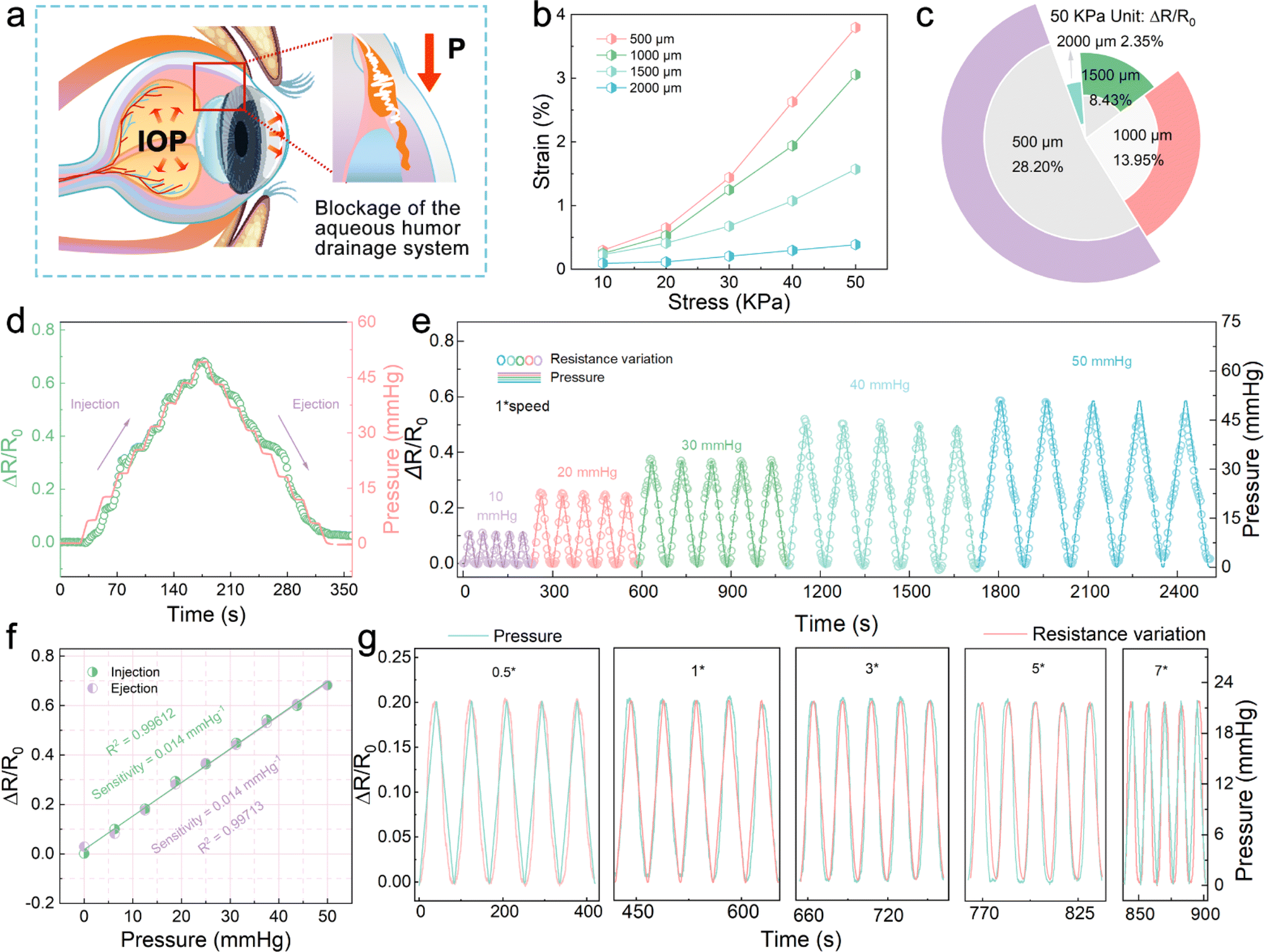 | ||
| Fig. 4 (a) Schematic diagram of the crystalline lens increased IOP. (b) Stress–strain curves of P(VDF-TrFE) membranes prepared at 1500 rpm with different widths. (c) ΔR/R0 values of the sensor at 50 kPa of tension with different widths of the P(VDF-TrFE) substrates. (d) Dynamic step response plot of the IOP sensor. (e) Plot of the response of the IOP sensor to resistance variation in different pressure conditions. (f) Resistance variation (ΔR) versus pressure change in the rising and falling phases of IOP. (g) Plot of the response of the IOP sensor to resistance variation at different pressure change rates. | ||
A hemispherical integrated device was assembled, consisting of an IOP sensor and Ti3C2Tx-MSCs, which can be used for self-powered real-time IOP monitoring. As shown in Fig. 5a, to obtain satisfactory sensitivity and stable driving voltage, a strategy of regulating the width and thickness of the P(VDF-TrFE) substrate is designed and adapted to achieve stress division. There is a plastic zone derived from a wide and thick P(VDF-TrFE) membrane as the substrate of Ti3C2Tx-MSCs, while there is an elastic zone derived from a narrow and thin P(VDF-TrFE) membrane as the substrate of the IOP sensor. The elastic zone allows for more appreciable stress concentration to respond quickly to various tiny stresses. However, the plastic zone is not expected to undergo greater deformation under the stress fields because the MSC requires constant electrode spacing and conductivity. Thus, the 3D FEA simulations of the joint area between the IOP sensor and Ti3C2Tx-MSCs, shown in Fig. 5b, were conducted to intuitively demonstrate the absorption state of the two regions divided by the applied stress. In addition, 2D FEA simulations were also carried out (Fig. S13†), which can further reveal the difference in the absorbed stress between the two ends of the joint. In Fig. 5c, a simple self-made IOP test rig, composed of a motor, pressure supply module, and manometer, combined with the designed equivalent circuit of the hemispherical integrated device to complete the IOP monitoring function together.
 | ||
| Fig. 5 (a) Schematic diagram showing the self-drive and stress division mechanism of the hemispherical integrated device. (b) FEA simulations for the device regarding the stress division. (c) Schematic of the human IOP simulation test rig. (d) CV curves of Ti3C2Tx-MSCs under different stress applied. (e) Digital photos of the device under various applied pressures. (f) Plot of the IOP sensor powered by Ti3C2Tx-MSCs respond to pressure cycles of 0 to 21 mmHg. (g) Plot of the IOP sensor response to pressure cycles from 0 to 22 mmHg at a voltage of 0.5 V. | ||
Therefore, the thickness of 193.25 μm and 37.68 μm P(VDF-TrFE) membranes was utilized as the substrates of the Ti3C2Tx-MSCs and IOP sensor, respectively. It cannot be ignored that the output performance of the Ti3C2Tx-MSCs module will inevitably be affected by the applied IOP when the hemispherical integrated device is put into test or practical use. Thus, the CV curves and EIS plots under different stress fields were obtained, as shown in Fig. 5d and S14.† As larger IOP values are applied to the device, the rectangular areas from the CV curves become smaller, and the EIS plots move in the direction of larger resistance values, which can be attributed to slower ion migration due to the wider electrode spacing. However, under the limit IOP value of 50 mmHg, the output capacitance retention of Ti3C2Tx-MSCs can reach 78% of the initial state, and it can still maintain 63% of the capacitance retention output even after 100 turns of applying and releasing pressure (Fig. S15†), which is sufficient to demonstrate that the Ti3C2Tx-MSCs module has acceptable and stable electrochemical performance against external forces.43 As shown in Fig. 5e, the image of the hemispherical integrated device under various applied stress fields shows that it can withstand any IOP values within the monitoring range and adapt to the curved surface requirements of human wear. Fig. S16† tests the self-discharge behavior of Ti3C2Tx-MSCs, and the discharge voltage can stay above 0.5 V for a long time. Meanwhile, the Ti3C2Tx-MSCs-driven strain sensors were tested for their continuous response to pressure variations (0–21 mmHg), verifying that the devices are capable of self-driven real-time monitoring of IOP changes (Fig. S17†). The capacitor-driven IOP strain sensor has a similar sensitivity to the 0.5 V voltage-driven sensor, revealing the effective voltage output value of the capacitor, as displayed in Fig. 5f, g and S18.† At the same time, it also confirms that the hemispherical integrated device can be used for the real-time monitoring of eye health, providing a convenient service for glaucoma and other high IOP diseases.
Conclusions
In summary, we successfully proposed a Ti3C2Tx MXene-based hemispherical integrated system with self-powered function to realize intraocular pressure monitoring. The high specific capacitance of 32 mF cm−2 at a scan rate of 5 mV s−1, energy density of 10 mW h cm−2, and hemispherical architectures of the Ti3C2Tx MXene-based MSC provide a robust energy supply for the strain sensors. The IOP strain sensor exhibits an excellent sensitivity of 0.014 mmHg−1 and a wide monitoring range from 0 to 50 mmHg. By integrating the MSC device and strain sensor on the same deformable substrate, the self-powered system successfully achieves an independent, continuous, and stable IOP monitor. Moreover, the facile design and fabrication process of the hemispherical devices paves a new way for the integration of various functional devices on the hemispherical curve, which will push the development of intelligent and multifunctional ocular devices.Conflicts of interest
There are no conflicts to declare.Acknowledgements
This work was supported by National Natural Science Foundation of China (52273256), Beijing Natural Science Foundation (L223006), Beijing Institute of Technology Research Found Program for Young Scholars and the BIT Research and Innovation Promoting Project (2023YCXZ010).Notes and references
- T. Grossmann and K. L. Dela Cruz, J. Behav. Brain Sci., 2021, 44, e155 CrossRef PubMed.
- X. Hou, L. Zhang, Y. Su, G. Gao, Y. Liu, Z. Na, Q. Xu, T. Ding, L. Xiao, L. Li and T. Chen, Nano Energy, 2023, 105, 108013 CrossRef CAS.
- X. Hou, L. Xin, Y. Fu, Z. Na, G. Gao, Y. Liu, Q. Xu, P. Zhao, G. Yan, Y. Su, K. Cao, L. Li and T. Chen, Nano Energy, 2023, 118, 109034 CrossRef CAS.
- C. Yang, Q. Wu, J. Liu, J. Mo, X. Li, C. Yang, Z. Liu, J. Yang, L. Jiang, W. Chen, H. Chen, J. Wang and X. Xie, Nat. Commun., 2022, 13, 2556 CrossRef CAS PubMed.
- J. Zhang, K. Kim, H. J. Kim, D. Meyer, W. Park, S. A. Lee, Y. Dai, B. Kim, H. Moon, J. V. Shah, K. E. Harris, B. Collar, K. Liu, P. Irazoqui, H. Lee, S. A. Park, P. S. Kollbaum, B. W. Boudouris and C. H. Lee, Nat. Commun., 2022, 13, 5518 CrossRef CAS PubMed.
- Y. Yang, X. Wei, W. Yao and J. Lan, Sens. Actuators, A, 2023, 364, 114819 CrossRef CAS.
- L. Gu, S. Poddar, Y. Lin, Z. Long, D. Zhang, Q. Zhang, L. Shu, X. Qiu, M. Kam, A. Javey and Z. Fan, Nature, 2020, 581, 278–282 CrossRef CAS PubMed.
- S. Chen, J. Qi, S. Fan, Z. Qiao, J. C. Yeo and C. T. Lim, Adv. Healthcare Mater., 2021, 10, 2100116 CrossRef CAS PubMed.
- J. Kim, M. Kim, M. S. Lee, K. Kim, S. Ji, Y. T. Kim, J. Park, K. Na, K. H. Bae, H. Kyun Kim, F. Bien, C. Young Lee and J. U. Park, Nat. Commun., 2017, 8, 14997 CrossRef PubMed.
- H.-W. Huang, J. Chen, P. R. Chai, C. Ehmke, P. Rupp, F. Z. Dadabhoy, A. Feng, C. Li, A. J. Thomas, M. Da Silva, E. W. Boyer and G. Traverso, Cyborg Bionic Syst., 2022, 11, 9780497 Search PubMed.
- J. Kim, J. Park, Y. G. Park, E. Cha, M. Ku, H. S. An, K. P. Lee, M. I. Huh, J. Kim, T. S. Kim, D. W. Kim, H. K. Kim and J. U. Park, Nat. Biomed. Eng., 2021, 5, 772–782 CrossRef PubMed.
- S. Guo, K. Wu, C. Li, H. Wang, Z. Sun, D. Xi, S. Zhang, W. Ding, M. E. Zaghloul, C. Wang, F. A. Castro, D. Yang and Y. Zhao, Matter, 2021, 4, 969–985 CrossRef CAS PubMed.
- H. Seo, Y. M. Hong, W. G. Chung, W. Park, J. Lee, H. K. Kim, S. H. Byeon, D. W. Kim and J. U. Park, Sci. Adv., 2024, 10, eadk7805 CrossRef CAS PubMed.
- Z. Liu, G. Wang, C. Ye, H. Sun, W. Pei, C. Wei, W. Dai, Z. Dou, Q. Sun, C. Lin, Y. Wang, H. Chen and G. Shen, Adv. Funct. Mater., 2021, 31, 2010991 CrossRef CAS.
- A. Hakim, B. Guido, L. Narsineni, D. W. Chen and M. Foldvari, Adv. Drug Delivery Rev., 2023, 196, 114781 CrossRef CAS PubMed.
- W. Zhang, L. Huang, R. N. Weinreb and H. Cheng, Mater. Des., 2021, 212, 110183 CrossRef.
- Z. Duan, M. Yuan, Z. Liu, W. Pei, K. Jiang, L. Li and G. Shen, Small, 2024, 2309785 CrossRef PubMed.
- B. Liu, Y. Peng, Y. Hao, Y. Zhu, S. Chang and S. Zhuang, PhotoniX, 2024, 5, 10 CrossRef.
- J. Reinhard, P. Urban, S. Bell, D. Carpenter and M. S. Sagoo, Nat. Commun., 2024, 15, 1360 CrossRef CAS PubMed.
- D. Kang, J. I. Lee, B. Maeng, S. Lee, Y. Kwon, M. S. Kang, J. Park and J. Kim, ACS Nano, 2022, 16, 15827–15836 CrossRef CAS PubMed.
- J. Park, D. B. Ahn, J. Kim, E. Cha, B. S. Bae, S. Y. Lee and J. U. Park, Sci. Adv., 2019, 5, eaay0764 CrossRef CAS PubMed.
- W. Liu, L. Li and G. Shen, Nanoscale, 2023, 15, 2624–2632 RSC.
- T. Iwase, T. Akahori, K. Yamamoto, E. Ra and H. Terasaki, Sci. Rep., 2018, 8, 17235 CrossRef PubMed.
- T. Y. Kim, J. W. Mok, S. H. Hong, S. H. Jeong, H. Choi, S. Shin, C. K. Joo and S. K. Hahn, Nat. Commun., 2022, 13, 6801 CrossRef CAS PubMed.
- A. VahidMohammadi, J. Moncada, H. Chen, E. Kayali, J. Orangi, C. A. Carrero and M. Beidaghi, J. Mater. Chem. A, 2018, 6, 22123–22133 RSC.
- W. Liu, C. Hu, L. Li and G. Shen, ACS Appl. Energy Mater., 2023, 6, 7387–7394 CrossRef CAS.
- Z. Du, W. Liu, J. Liu, Z. Chu, F. Qu, L. Li and G. Shen, Adv. Mater. Interfaces, 2023, 10, 2300266 CrossRef CAS.
- X. Hu, Y. Jiang, Z. Ma, Q. He, Y. He, T. Zhou and D. Zhang, ACS Appl. Polym. Mater., 2020, 2, 4399–4404 CrossRef CAS.
- Y. Park, Y. E. Shin, J. Park, Y. Lee, M. P. Kim, Y. R. Kim, S. Na, S. K. Ghosh and H. Ko, ACS Nano, 2020, 14, 7101–7110 CrossRef CAS PubMed.
- Z. Hu, J. Li, X. Wei, C. Wang, Y. Cao, Z. Gao, J. Han and Y. Li, ACS Appl. Mater. Interfaces, 2022, 14, 45853–45868 CrossRef CAS PubMed.
- H. Seo, W. G. Chung, Y. W. Kwon, S. Kim, Y. M. Hong, W. Park, E. Kim, J. Lee, S. Lee, M. Kim, K. Lim, I. Jeong, H. Song and J. U. Park, Chem. Rev., 2023, 123, 11488–11558 CrossRef CAS PubMed.
- L. Li, W. Liu, K. Jiang, D. Chen, F. Qu and G. Shen, Nano-Micro Lett., 2021, 13, 100 CrossRef CAS PubMed.
- W. Liu, L. Li, C. Hu, D. Chen and G. Shen, Adv. Mater. Technol., 2022, 7, 2200158 CrossRef CAS.
- N. Kurra, B. Ahmed, Y. Gogotsi and H. N. Alshareef, Adv. Energy Mater., 2016, 6, 1601372 CrossRef.
- Y. Y. Peng, B. Akuzum, N. Kurra, M. Q. Zhao, M. Alhabeb, B. Anasori, E. C. Kumbur, H. N. Alshareef, M. D. Ger and Y. Gogotsi, Energy Environ. Sci., 2016, 9, 2847–2854 RSC.
- Y. Liu, J. Yu, D. Guo, Z. Li and Y. Su, J. Alloys Compd., 2020, 815, 152403 CrossRef CAS.
- N. Wang, J. Liu, Y. Zhao, M. Hu, R. Qin and G. Shan, ChemNanoMat, 2019, 5, 658–665 CrossRef CAS.
- C. Zhang, M. P. Kremer, A. Seral Ascaso, S. Park, N. McEvoy, B. Anasori, Y. Gogotsi and V. Nicolosi, Adv. Funct. Mater., 2018, 28, 1705506 CrossRef.
- R. Li, L. Li, R. Jia, K. Jiang, G. Shen and D. Chen, Small Methods, 2020, 4, 2000363 CrossRef CAS.
- C. Yang, X. Huang, X. Li, C. Yang, T. Zhang, Q. Wu, D. Liu, H. Lin, W. Chen, N. Hu and X. Xie, Adv. Sci., 2021, 8, 2002971 CrossRef CAS PubMed.
- Y. Fan, H. Tu, H. Zhao, F. Wei, Y. Yang and T. Ren, Nanotechnology, 2021, 32, 095106 CrossRef CAS PubMed.
- M. Yuan, Z. Liu, X. Wu, H. Gou, Y. Zhang, X. Ning, W. Li, Z. Yao, Y. Wang, W. Pei and H. Chen, Sens. Actuators, A, 2023, 354, 114250 CrossRef CAS.
- M. O. Bamgbopa, D. Belaineh, D. A. Mengistie, J. Edberg, I. Engquist, M. Berggren and K. Tybrandt, J. Mater. Chem. A, 2021, 9, 2184–2194 RSC.
Footnote |
| † Electronic supplementary information (ESI) available. See DOI: https://doi.org/10.1039/d4ta02127d |
| This journal is © The Royal Society of Chemistry 2024 |