 Open Access Article
Identification of distinctive structural and optoelectronic properties of Bi2O3 polymorphs controlled by tantalum addition†
Taro
Saito‡
a,
Rafia
Ahmad‡
b,
Fuminao
Kishimoto
 a,
Tomohiro
Higashi
 c,
Masao
Katayama
d,
Luigi
Cavallo
 *b and
Kazuhiro
Takanabe
 *a
*a
aDepartment of Chemical System Engineering, School of Engineering, The University of Tokyo, 7-3-1, Hongo, Bunkyo-ku, Tokyo 113-8656, Japan. E-mail: takanabe@chemsys.t.u-tokyo.ac.jp
bKing Abdullah University of Science and Technology (KAUST), KAUST Catalysis Center (KCC), 4700 KAUST, Thuwal 23955-6900, Saudi Arabia
cInstitute for Tenure Track Promotion, University of Miyazaki, Nishi 1-1 Gakuen-Kibanadai, Miyazaki 889-2192, Japan
dEnvironmental Science Center, Department of Chemical System Engineering, The University of Tokyo, 7-3-1, Hongo, Bunkyo-ku, Tokyo 113-8656, Japan
First published on 25th November 2022
Abstract
Diverse crystal phases of bismuth (Bi) oxides induced by the addition of different amounts of tantalum (Ta) were synthesized. Their optoelectronic and redox properties were quantitatively investigated using combined experimental and computational approaches. Synthesis conditions that transform α-Bi2O3 into β-Bi2O3 and δ-Bi2O3 in terms of the Ta quantity, as well as synthesis temperatures, are identified and demonstrated. The phase transition behavior and crystal structures were characterized by in situ high temperature X-ray diffraction (XRD), thermogravimetry–differential thermal analysis (TG/DTA), X-ray absorption near edge structures (XANES), and extended X-ray absorption fine structures (EXAFS). Density functional theory calculations employing the HSE exchange–correlation functional with spin–orbit coupling were used to quantitatively simulate the optoelectronic properties and band structures of β-Bi2O3 and δ-Bi2O3. Along with the absorption coefficient and density of states, effective masses and dielectric constants were elucidated. The characterization study confirmed the distortion of Ta–O bonds in the Ta-supplemented β-Bi2O3 and the substitutional positions of the Bi and Ta atoms in the δ-Bi2O3 and Bi3TaO7 compounds. The reducibility of these oxides was strongly influenced by the crystal phase confirmed by temperature-programmed reduction (TPR) analysis. These findings can be used as a bismuth oxides' benchmark for optoelectronic applications as well as thermal catalysis as the redox active center or the support.
Introduction
Bi2O3 is one of the polymorphous oxides, and is employed in a broad range of applications such as solid-state electrocatalysis,1–6 inorganic orange pigment,7 and photocatalytic reactions.8–27 To date, four different crystal phases have been reported: α phase (monoclinic), β phase (tetragonal), γ phase (cubic), and δ phase (cubic). Among the polymorphs, the α phase is the most stable phase at room temperature. The high-temperature–stable δ phase is transformed into the β or γ phase while cooling, which results in the further transformation into the α phase at room temperature.28 While the δ phase shows a high O2− ion conductivity, applicable to mid-temperature electrocatalysis at 300–500 °C,1–5 β-Bi2O3 attracts attention as a photocatalyst due to a narrow bandgap of ∼2.2 eV.8–12Solid-state synthesis of pure Bi2O3 has been well reported in the literature.28 Knowing the melting point of Bi2O3 to be ∼830 °C, phase transition temperatures have been studied in detail. Nevertheless, selective synthesis of specific phases from pure Bi2O3 remains challenging. By doping α-Bi2O3 with a trace amount of oxides, such as Ta2O5, CeO2, ZrO2, EuOx, TiOx, and MnOx,5,7,29–33 a solid-state reaction at a high temperature becomes possible to make metastable β-, γ-, and δ-phases recoverable for successive applications. Recently, Masui and coworkers reported the addition of Ta2O5 into α-Bi2O3 to synthesize β- and δ-phases, and among them, β-Bi2O3 was recognized to have a potential to be a orange pigment with its vivid orange color due to its unique bandgap narrowing.7 This bandgap with a visible light response may be suitable for solar energy conversion, but the investigation of β-Bi2O3 as a photocatalyst, especially for application in photosynthetic reactions, has been limited.9 The details of how Ta induces the crystal phase transition and narrows the bandgap also remain unclarified.
The purpose of this study is to provide not only explicit synthesis protocols for each crystal structure, but also quantitatively analyse various optoelectronic and redox properties of bismuth oxides. Different Bi2O3 phases and Bi3TaO7 were successfully achieved by varying the Ta/Bi ratio (0.020–0.333). The obtained materials were characterized by in situ X-ray diffraction (XRD), X-ray absorption spectroscopy (XAS), diffuse-reflectance ultraviolet-visible spectroscopy (DR-UV-vis), and photoelectron spectroscopy in air (PESA). The optoelectronic structure was studied both experimentally and theoretically to understand their density of states (DOS), dielectric properties, and effective masses. Photoelectrochemical (PEC) measurements and temperature-programmed reduction (TPR) analyses were conducted.
Experimental and theoretical
Synthesis
Ta2O5 (99.9%, Kojundo Chemical Laboratory Co., Ltd.) was mixed with Bi2O3 (98.0+%, FUJIFILM Wako Pure Chemical Corporation) (0.020 ≤ Ta/Bi ≤ 0.333) using a mortar and pestle. Heat treatment was usually conducted at 850 °C, with a heating rate of 10 °C min−1 and was held at this temperature for 5 h in a muffle furnace in air. During the heat treatment, the mixtures were placed on an Alumina boat (Nikkato, SSA-S grade, Al2O3 99.6%) to prevent contamination of silica components. Then, the samples were cooled naturally in the furnace by turning off the electric power. The samples were ground in an Alumina boat prior to characterization.X-ray diffraction
The powder XRD patterns were collected using a Rigaku Ultima III equipped with a copper (Cu) X-ray source operated at 40 kV and 40 mA. The diffractometer was configured with a 1/2° divergence slit limited to 10 mm, an open scattering slit, an open receiving slit, and a nickel (Ni) filter to attenuate contributions from Cu-Kβ fluorescence. The data sets were acquired in continuous scanning mode (20° min−1) with an integration step size of 0.02°; however, when focusing on certain peaks (i.e., only around 2θ = 26–29°), these parameters were set to 1° min−1 and 0.01°, respectively. The peak positions were calibrated using the secondary peak of silicon (Si) (standard, 220, 47.2660°, cubic, Fd![[3 with combining macron]](https://www.rsc.org/images/entities/char_0033_0304.gif) m). In situ high-temperature XRD was performed using an attachment (Reactor-X, Rigaku) equipped with an infrared heater connected to its controller (PTC EVO, Rigaku) and an external power source (Thermo plus EVO PU-4K CE, Rigaku). An infrared reflector was attached to assist in heating the sample, while the attachments were continuously cooled with circulating water and both an external and internal fan. With this setup, the peak positions were calibrated using the secondary peak of Si powder (Wako, 220, 47.2660°, cubic, Fd
m). In situ high-temperature XRD was performed using an attachment (Reactor-X, Rigaku) equipped with an infrared heater connected to its controller (PTC EVO, Rigaku) and an external power source (Thermo plus EVO PU-4K CE, Rigaku). An infrared reflector was attached to assist in heating the sample, while the attachments were continuously cooled with circulating water and both an external and internal fan. With this setup, the peak positions were calibrated using the secondary peak of Si powder (Wako, 220, 47.2660°, cubic, Fd![[3 with combining macron]](https://www.rsc.org/images/entities/char_0033_0304.gif) m) at room temperature. The temperature was increased with a heating rate of 10 °C min−1 from room temperature to 830 °C and 2 °C min−1 from 830 °C to 850 °C to prevent the cell from overheating. The temperature was decreased with a cooling rate of 10 °C min−1 to 25 °C, and the determined temperature was held for 5 min before each measurement. All measurements were conducted by flowing a mixture of 80 mL min−1 argon (Ar) and 20 mL min−1 O2. The temperature was corrected by using the α to δ phase transition peak (in the heating process) of Bi2O3 (98.0+%, Wako Pure Chemical Corporation) at 735 °C.
m) at room temperature. The temperature was increased with a heating rate of 10 °C min−1 from room temperature to 830 °C and 2 °C min−1 from 830 °C to 850 °C to prevent the cell from overheating. The temperature was decreased with a cooling rate of 10 °C min−1 to 25 °C, and the determined temperature was held for 5 min before each measurement. All measurements were conducted by flowing a mixture of 80 mL min−1 argon (Ar) and 20 mL min−1 O2. The temperature was corrected by using the α to δ phase transition peak (in the heating process) of Bi2O3 (98.0+%, Wako Pure Chemical Corporation) at 735 °C.
X-ray absorption spectroscopy
Bi L3-edge and Ta L3-edge XAS were performed at the bending magnet XAFS beamline, BL01B1 at SPring-8 (Hyogo, Japan). Experiments were performed at room temperature and in the transmission mode using the ionization chambers. Bi2O3 and Ta2O5 were used as references. The powder samples were thoroughly ground with boron nitride in an agate mortar, and 10 mm–diameter pellets were made. The amount of boron nitride was ∼90 mg to ensure that the pellets could be handled without breaking. The EXAFS spectra were analyzed using the HORAE-IFEFFIT (Athena) program package. This program enabled us to normalize the absorption coefficient, μ(k), and to separate the oscillatory EXAFS, χ(k), from the absorption background. Before normalization, the pre-edge range of the spectra for Bi and Ta L3 edges was flattened in the energy range of −210 to −60 keV and −200 to −60 keV, respectively. The data sets for Bi and Ta L3 edges were normalized in the energy range of 50–880 keV (4.0–71.0 Å−1) and 200–1000 eV (16.1–80.7 Å−1), respectively. Then, the background was calculated from the data in energy ranges of 0–15 Å−1 (0–857 eV) for Bi L3 edges and 0–17 Å−1 (0–1001 eV) for Ta L3 edges. All data were Fourier-transformed using the same k range, k = 3 – 12 Å−1, k weighting of 2 and a hanning k window and plotted with k weighting of 3. The theoretical radial distribution functions were calculated using the Visual Molecular Dynamics (VMD) program (version 1.9.4a49).34Band position determination
DR-UV-vis and PESA were performed to determine the band alignment of the conduction band minimum (CBM) and the valence band maximum (VBM) positions of the synthesized samples. DR-UV-vis spectroscopy was performed on a JASCO model V-770 spectrophotometer equipped with an integrating sphere. The reflectance spectra were scanned over the range of 200–1000 nm with a scan speed of 400 nm min−1 and a bandwidth of 2.0 nm for the ultraviolet/visible region and 8.0 nm for the near-infrared region. The reflectance spectra were referred to the background reflectance of BaSO4 powder. The contributions of scattering were removed by the Kubelka–Munk function, F(R∞). Followed by the calculation of the bandgap energy, the absorption edge was determined by the intercept of the straight line extrapolated to the F(R∞) vs wavelength.The valence band positions were determined by PESA (AC-3 photoelectron spectrometer, Riken Keiki Co., Ltd.). The obtained spectra were calibrated based on the work function of gold (Au) (5.30 eV vs. vacuum).35 The yield of the photoelectrons was measured for 30 s at every 0.1 eV step in the range of 4.0–7.0 eV of irradiation UV light. The valence band potentials, obtained as the potentials relative to the absolute vacuum potential, were converted to the standard hydrogen potentials (ESHE = Eabs − 4.44 V). The conduction band positions were calculated from the valence band positions, and the bandgaps were determined by PESA and DR-UV-vis spectroscopy.
Photoluminescence
Photoluminescence (PL) spectroscopy was performed on a JASCO model FP-8500 fluorescence spectrometer operated at liquid nitrogen temperature under ambient pressure. The excitation and emission had a 5 nm bandwidth. The spectra were scanned at a speed of 1000 nm min−1 with medium level sensitivity and 50 ms of response at every 0.1 nm interval and accumulated over 10 cycles.Thermogravimetry/differential thermal analysis
TG/DTA was performed to investigate the phase transition processes of Ta2O5-supplemented Bi2O3in situ. TG/DTA was performed using a Thermo plus EVO2 series TG-DTA 8120 (Rigaku) in the atmosphere of the residual air in the chamber without flow. All measurements were performed with a 10 °C min−1 heating rate and cooling rates of up to 850 °C. The sample (8–10 mg of the Bi2O3 powder or the mixture of Bi2O3 and Ta2O5 powders mixed at the stoichiometric amounts [Ta/Bi = 0.05, 0.10]) was placed in an open platinum pan. An open and empty platinum pan was used as the reference.Scanning electron microscopy (SEM) and elemental analysis
The morphologies, particle sizes, and the layered structure of the particulate photoelectrodes were examined using a high-resolution field emission SEM (FE-SEM; JEOL, JSM-IT800) equipped with a secondary electron detector. Energy-dispersive X-ray spectroscopy (EDS) was conducted with an EDS detector (Ultim Max, Oxford Instruments).Computational method
All calculations were performed using the Vienna Ab initio Simulation Package (VASP),36,37 with the projector augment wave (PAW) method.38 Calculations were performed with the cut-off energy set to 400![[thin space (1/6-em)]](https://www.rsc.org/images/entities/char_2009.gif) eV. Brillouin zone sampling was performed using Monkhorst and Pack schemes.39 We completely relaxed the bulk unit cell of β-Bi2O3 in its tetragonal structure with space group P
eV. Brillouin zone sampling was performed using Monkhorst and Pack schemes.39 We completely relaxed the bulk unit cell of β-Bi2O3 in its tetragonal structure with space group P![[4 with combining macron]](https://www.rsc.org/images/entities/char_0034_0304.gif) 21c, which contains 8 Bi atoms and 12 oxygen (O) atoms. δ-Bi2O3 has a cubic fluorite structure with a space group of Fm3m. The unit cell contains two Bi2O3 formulas. The valence atomic configurations are 5d10 6s2 6p3 for Bi and 2s2 2p4 for O atoms. Geometry optimizations were terminated when the energy and force on each ion were reduced below 10−6 eV and 0.02 eV Å−1, and the optimized structures were then used to calculate the electronic structures. Hybrid DFT calculations were performed at a single point at the generalized gradient approximation (GGA) lattice geometry.40 First, the GGA scheme was employed for the fully-relaxed structural optimization. Then, the screened-exchange hybrid functional of Heyd, Scuseria, and Ernzerhof (HSE06),41,42 representing the electronic exchange–correlation energy, was adopted for calculations of the electronic and optical properties. The spin–orbit coupling (SOC) effect was taken into consideration through the second variational method because of the relativistic effect in Bi atoms.43 More details of the computational modeling of surfaces and of the methodology used to calculate the optical properties can be found in the ESI.†
21c, which contains 8 Bi atoms and 12 oxygen (O) atoms. δ-Bi2O3 has a cubic fluorite structure with a space group of Fm3m. The unit cell contains two Bi2O3 formulas. The valence atomic configurations are 5d10 6s2 6p3 for Bi and 2s2 2p4 for O atoms. Geometry optimizations were terminated when the energy and force on each ion were reduced below 10−6 eV and 0.02 eV Å−1, and the optimized structures were then used to calculate the electronic structures. Hybrid DFT calculations were performed at a single point at the generalized gradient approximation (GGA) lattice geometry.40 First, the GGA scheme was employed for the fully-relaxed structural optimization. Then, the screened-exchange hybrid functional of Heyd, Scuseria, and Ernzerhof (HSE06),41,42 representing the electronic exchange–correlation energy, was adopted for calculations of the electronic and optical properties. The spin–orbit coupling (SOC) effect was taken into consideration through the second variational method because of the relativistic effect in Bi atoms.43 More details of the computational modeling of surfaces and of the methodology used to calculate the optical properties can be found in the ESI.†
Electrochemical (EC) and photoelectrochemical (PEC) measurements
To conduct EC and PEC measurements, particulate photoelectrodes were fabricated through previously reported particle transfer methods.44 Multilayers of photocatalyst particles were deposited on a glass plate by drop-casting and drying its suspension in isopropanol several times, resulting in an approximate amount of 10 mg cm−2. Subsequently, 200 nm-thick–Ti and 3–4 μm–thick-Sn were sequentially deposited on the particles through electron beam deposition (ULVAC) to prepare the assembly of photocatalysts with a Ti–Sn conductive layer. The obtained assembly of particles and the Ti–Sn layer adhering to them were peeled off from the glass plate, and the excess unused particles piled up on the deposited particles were removed by ultrasonication in ethanol. The film electrode was fixed on another glass plate using carbon tape. Finally, the film was connected to lead wire using an indium solder, after which its unnecessary part was covered with epoxy resin for insulation. The geometrical electrode areas of the photoelectrodes were approximately 0.20–0.30 cm2. EC and PEC measurements for the particulate-photoelectrodes were performed using a three-electrode system under an argon (Ar) gas atmosphere at a temperature of 25 °C. The Hg/Hg2Cl2/saturated KCl reference electrode (BAS Inc., RE-2BP, 241 mV vs. RHE at 25 °C) and coiled-Pt wire counter electrode were connected to a potentiostat (SP-150, BioLogic Science Instruments). Prior to the PEC measurements, a CoOx catalyst promoting the carrier transfer at the solid–liquid interface was electrodeposited under light irradiation on the surface of the particulate photoelectrodes. A solar simulator (XES-40S2, SAN-EI Electric Co., Ltd.) equipped with an AM 1.5G filter was used as the light source, and the light intensity was adjusted to 100 mW cm−2 (1 sun). The electrolyte was made by saturating Co(NO3)2·6H2O (0.1 M, 99.5%, Wako) in a 1 M potassium phosphate buffer solution. The pH of the buffer was adjusted to 7.0 by adding a potassium hydroxide (KOH; >85%, Sigma-Aldrich) solution into a phosphoric acid (H3PO4, ≥ 85 wt% in H2O, Sigma-Aldrich) aqueous solution. Electrodeposition was performed at a constant current density of 50 μA cm−2 for 5 min under simulated solar light (AM 1.5G). CoOx deposited or not deposited particle-transferred working electrodes with an area of approximately 0.2–0.3 cm2 were positioned in a glass cell. The electrolyte was a 1M potassium borate buffer (pH 9.0) aqueous solution. The pH was adjusted to 9.0 by adding a KOH (≥85%, Sigma-Aldrich) solution into a boric acid (H3BO3, ≥99.5 wt% in H2O, Sigma-Aldrich) aqueous solution. For LSV measurements, 0.1 M of Na2SO3 was added as a hole scavenger. PEC measurements employed a Xe-lamp (MAX-303 Xenon Light Source, 300 W, Asahi Spectra), with a UV-Vis miler module and a cut-off filter (HOYA L42) as the light source (420 < λ < 650 nm).Temperature-programmed reduction
TPR equipment consisted of mass flow controllers (KOFLOC, model 3660) and a U-shaped quartz reactor inside an oven. Samples were treated in flowing Ar (20 mL min−1) by increasing their temperature to 400 °C at 40 °C min−1 and holding for 1 h. After cooling to room temperature, the Ar stream was replaced with the reducing gas, 4% H2 in Ar (20 mL min−1). The temperature was increased with a heating rate of 10 °C min−1 from room temperature to 850 °C, and the H2 concentration was monitored using a GC (GC-8A, TCD, Shimadzu) connected to the outlet of the reactor.Results and discussion
Synthesis and structural characterization of β- and δ-Bi2O3 and Bi3TaO7
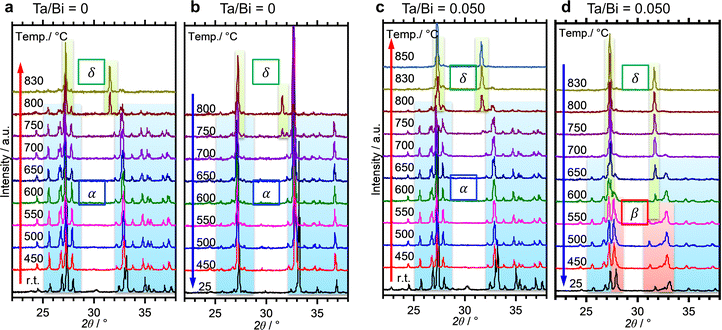
The formation process of the β-Bi2O3:Ta (5%) and the δ-Bi2O3:Ta (10%) in the solid-state reaction was studied by DTA and in situ high temperature XRD measurements. Fig. 1 shows the DTA curves of the pure Bi2O3, mixture of Bi2O3 and Ta2O5 at ratios of Ta/Bi of 0.05 and 0.10. Fig. 2 shows the in situ high temperature XRD patterns for the samples at Ta/Bi = 0 (Fig. 2a and b) and 0.050 (Fig. 2c and d). Upon heating the samples, all of the samples show endothermic peaks at 735 °C (Fig. 1). Accordingly, the new peak assignable to δ-Bi2O3 appeared (Fig. 2a), clearly indicating the α to δ transition at this temperature. Pure Bi2O3 shows an additional endothermic peak at 830 °C, which can be attributed to the melting of δ-Bi2O3.28 Lack of melting behavior with Ta addition suggests that the melting point of Bi2O3 is higher than 850 °C. Subsequent decreases in the temperature provided substantial differences in phase transition by varied Ta addition. For pure Bi2O3 (Ta/Bi = 0), in Fig. 1, the DTA curve in the cooling process shows two exothermic peaks of curding at 830 °C and at 620 °C. As the peak at 830 °C is likely ascribed to solidification, consistent with the literature,28in situ XRD measurements clearly identified that a δ-to-α transition occurred (Fig. 2b), indicating that the original state was recovered during the heating–cooling cycle. For the sample with Ta/Bi = 0.050, an exothermic peak at 580 °C (Fig. 1) corresponds to the δ-to-β transition (Fig. 2d), the phase that was not obtained without Ta addition. For the sample with Ta/Bi = 0.100, the DTA curve (Fig. 1) did not show any pronounced peaks while cooling. This indicates that the δ phase of the Ta-supplemented Bi2O3 was maintained during the cooling process.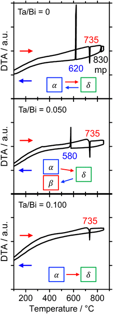 | ||
| Fig. 1 DTA curves of the Bi2O3 samples with Ta/Bi ratios of 0, 0.050, and 0.100. The temperature was increased and subsequently decreased at the rate of 10 °C min−1 in flowing air. | ||
Fig. 3a shows the XRD patterns of the samples with a much wider range of Ta/Bi ratios after cooling from the heat treatment at 850 °C for 5 h. Fig. 3b shows the schematics of the corresponding various crystal structures. The XRD patterns of α-, β-, δ-Bi2O3 and Bi3TaO7 from the inorganic crystal structure database (ICSD) are shown in Fig. S1 (ESI†) as references. While no Ta2O5 addition led to the formation of the monoclinic α-Bi2O3 structure, a small addition of Ta (Ta/Bi ratio from 0.020 to 0.050) led to the formation of the β-Bi2O3 (tetragonal) structure. Further addition of Ta, to give rise to Ta/Bi ratio of 0.100, led to the formation of the δ phase of Bi2O3 (cubic, Pn![[3 with combining macron]](https://www.rsc.org/images/entities/char_0033_0304.gif) m). The samples with Ta/Bi = 0.167 and 0.333 were identified as the Bi3TaO7 phase (cubic, F
m). The samples with Ta/Bi = 0.167 and 0.333 were identified as the Bi3TaO7 phase (cubic, F![[3 with combining macron]](https://www.rsc.org/images/entities/char_0033_0304.gif) m). The principal XRD peaks of the obtained β-Bi2O3, δ-Bi2O3, and Bi3TaO7 phases are highlighted in Fig. S2 (ESI†). It is of great significance to note that the amount of Ta from 2–5% did not influence the peak position of β-Bi2O3, suggesting that the Bi and Ta atoms do not replace each other in the crystal structures of our Ta-supplemented β-Bi2O3 samples in a way that affects the lattice constant. On the other hand, for Bi3−xTaxO3+y (x = 1.29) and Bi3TaO7 with the Ta/Bi ratios of 0.167 and 0.333 (Fig. S2b, ESI†), the main XRD peaks for the (111) plane can be explained by the replacement of a Ta5+ cation with a Bi3+ cation, which is accompanied by the creation of oxygen vacancies for the charge compensation, and the overall charge electroneutrality of the system is preserved through a mechanism: Bi3+ +mpe5+ + O2−.6 Finally, the studied samples are compiled in Table 1.
m). The principal XRD peaks of the obtained β-Bi2O3, δ-Bi2O3, and Bi3TaO7 phases are highlighted in Fig. S2 (ESI†). It is of great significance to note that the amount of Ta from 2–5% did not influence the peak position of β-Bi2O3, suggesting that the Bi and Ta atoms do not replace each other in the crystal structures of our Ta-supplemented β-Bi2O3 samples in a way that affects the lattice constant. On the other hand, for Bi3−xTaxO3+y (x = 1.29) and Bi3TaO7 with the Ta/Bi ratios of 0.167 and 0.333 (Fig. S2b, ESI†), the main XRD peaks for the (111) plane can be explained by the replacement of a Ta5+ cation with a Bi3+ cation, which is accompanied by the creation of oxygen vacancies for the charge compensation, and the overall charge electroneutrality of the system is preserved through a mechanism: Bi3+ +mpe5+ + O2−.6 Finally, the studied samples are compiled in Table 1.
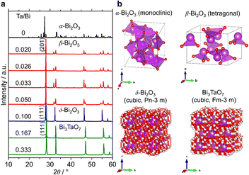 | ||
| Fig. 3 (a) XRD patterns of the samples at the Ta/Bi ratio. B) Schematics of the crystal structures from ICSD 94229 (α-Bi2O3), 417638 (β-Bi2O3), 38436 (δ-Bi2O3), and 161407 (Bi3TaO7). | ||
| Ta/Bi ratio | Crystal phase | Notation |
|---|---|---|
| 0 | α-Bi2O3 (monoclinic) | α-Bi2O3 (precursor) |
| 0.020 | β-Bi2O3 (tetragonal) | β-Bi2O3:Ta (2%) |
| 0.026 | β-Bi2O3 (tetragonal) | β-Bi2O3:Ta (2.6%) |
| 0.033 | β-Bi2O3 (tetragonal) | β-Bi2O3:Ta (3.3%) |
| 0.050 | β-Bi2O3 (tetragonal) | β-Bi2O3:Ta (5%) |
| 0.100 | δ-Bi2O3 (cubic, Pn![[3 with combining macron]](https://www.rsc.org/images/entities/char_0033_0304.gif) m) m) |
δ-Bi2O3:Ta (10%) |
| 0.167 | Bi3TaO7 (cubic, Fm![[3 with combining macron]](https://www.rsc.org/images/entities/char_0033_0304.gif) m) m) |
Bi3+xTa1–xO7–y (x = 0.43) |
| 0.333 | Bi3TaO7 (cubic, Fm![[3 with combining macron]](https://www.rsc.org/images/entities/char_0033_0304.gif) m) m) |
Bi3TaO7 |
| — | Ta2O5 (orthorhombic) | Ta2O5 (precursor) |
Fig. S3 (ESI†) shows the SEM images and EDS mappings of the representative samples. Aggregated coarse particles with sizes on the order of micrometers somewhat thermally fused were observed in all samples. From EDX mapping, it can be observed that Bi, Ta, and O are well distributed throughout the particles for all samples, indicating the formation of a homogeneous solid solution or Ta-doped Bi2O3.
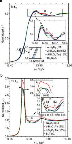
A small amount of added Ta was observed to play a significant role in structural determination. To identify at which positions the Ta atoms are located in the crystal structures, the local environments of Bi and Ta atoms were studied with XAS measurements, including XANES and EXAFS. All spectra and their analyses are summarized in Fig. S4 (ESI†). The Bi L3-edge XANES spectra of α-Bi2O3 (reference), β-Bi2O3:Ta (5%), δ-Bi2O3:Ta (10%), and Bi3TaO7 are shown in Fig. 4a. The spectral shape of the samples basically consists of a main absorption peak (A) located at 13.445 eV, a slight shoulder-like structure just below the main peak (A1, hν ∼ 13.42 keV), and a single oscillation after the main peak (B, hν ∼ 13.46 keV). The spectra of β-Bi2O3:Ta (5.0%), δ-Bi2O3:Ta (10.0%), and Bi3TaO7 show a hump (B, hν ∼ 13.46 keV) followed by a negative feature at higher energies (C, hν ∼ 13.47 keV), and the spectrum of α-Bi2O3 presents a wide plateau in the energy region immediately after the main peak (B–C, hν ∼ 13.46–13.47 keV). This directly indicates that the local environments of Bi in the samples under study are different from those of α-Bi2O3. Moreover, the shift in the shoulder-like structure (A1, hν ∼ 13.42 keV) at the edge (A, hν ∼ 13.445 keV) and just below the edge (B, hν ∼ 13.46 keV) cannot be explained with the linear combination of each other. In other words, the XANES profiles of the samples cannot be explained with the presence of mixed polymorphs.
Next, the Ta L3-edge XANES spectra of α-Bi2O3 (reference), β-Bi2O3:Ta (5%), δ-Bi2O3:Ta (10%), and Bi3TaO7 are shown in Fig. 4b. All of the compounds show a main peak (A) at ∼9.884 keV, but our samples have a double peak corresponding to the split of 5d orbitals, whereas the Ta2O5 reference shows only a single peak. This difference is more apparent in the energy region immediately after the main peak because our samples show a hump (B, hν ∼ 9.906 keV), whereas the Ta2O5 reference only shows a shoulder-like structure (B1, hν ∼ 9.903 keV) followed by a negative feature at a higher energy (B2, hν ∼ 9.910 keV). These comparisons to the Ta2O5 reference show that the local environments around Ta in our studied samples are different from those in the Ta2O5 reference. Similar results are reported in the W L3-edge XANES spectra of Bi2WO6 (octahedral) and Bi14WO24 (tetrahedral) by Wind and coworkers29 and the W L3-edge XANES spectra of other W-related oxides by Yamazoe and coworkers.44 It is reasonable to consider that the differences of the local environments around Ta in the Ta2O5 (reference) and our Bi–Ta oxides result from a distortion or oxygen vacancies in the crystal structure induced by Ta addition.
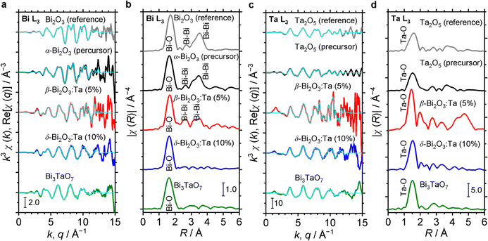
The characteristics of the structural orders around Bi and Ta in the samples are also inferred from the comparison of the Fourier transforms of the EXAFS signals. In Fig. 5, Bi L3 and Ta L3 signals of Bi and Ta in the α-Bi2O3 reference, α-Bi2O3 precursor, and β-Bi2O3:Ta (5%) are compared. The main peak at ∼1.7 Å and double peaks at ∼3 Å shown in Fig. 5b correspond to the first coordination shell made of oxygen atoms and Bi neighbors.45 Additionally, these peaks could be explained by the theoretical radial distribution function calculated from the optimized crystal structures. Fig. 5c shows the Ta L3-edge EXAFS spectra of the Ta2O5 reference, Ta2O5 precursor, and β-Bi2O3:Ta (5%). The difference between the environments of Ta atoms in the Ta2O5 and our β-Bi2O3:Ta (5%) is suggested by the Fourier transforms shown in Fig. 5d. The enhancement of the main peak (∼1.5 Å) can be related to the distortions in distances and angles between the Ta–O bonds in the TaO6 octahedra.46 Furthermore, this distortion is also suggested by the shift of the main peak (∼1.5 Å) and appearance of the second peak at ∼2 Å.
The structural orders in the δ-Bi2O3:Ta (10%) and Bi3TaO7 and their crystal systems were also studied using both Bi L3 and Ta L3 edge EXAFS spectra. The EXAFS spectra are shown in Fig. 5a and c and their Fourier transforms are shown in Fig. 5b and d. To perform the theoretical simulation, we assumed that when a Ta atom substitutes Bi sites in the cubic lattice in such a way, that the Bi–O distance decreases, the O atoms move close to Bi. This substitutability of Bi and Ta leads to tunability of the bandgap of these cubic-phase B–Ta oxides, as is discussed later. One might initially contend that Ta5+ and Bi3+ cannot substitute each other in the crystal lattice because the charge in the oxide cannot be balanced. However, the charge has been reasonably explained to be balanced by the change in the occupancy of O sites in previous studies.5 Therefore, it can be concluded that by mixing Bi2O3 and Ta2O5 at a molar ratio of Ta/Bi = 0.1, 0.33, the resulting Bi–Ta oxides stabilized and formed a substitutional solid solution with the cubic crystal phase.
Electronic structures and optical properties
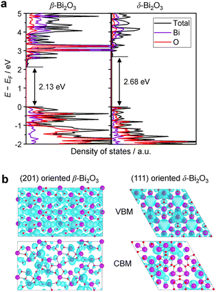
The densities of states (DOS) and the charge density maps of β-Bi2O3(201) and δ-Bi2O3(111) slabs were computed using the HSE06 (Heyd–Scuseria–Ernzerhof) exchange–correlation functional, and they are shown in Fig. 6a. The VBM is dominated by O 2p states, whereas the CBM is mostly composed of O 3s and Bi 6p for β-Bi2O3 and Bi 6p for δ-Bi2O3. It is worth mentioning that the narrower bandgaps of β-Bi2O3 and δ-Bi2O3 were explained only by Bi and O, without contribution from the partial density of states of Ta. To study the qualitative nature of chemical bonding in the (201) slab of β-Bi2O3 and the (111) slab of δ-Bi2O3, the electron density distribution is presented in Fig. 6b. Comparing these two model surfaces, we observe more depletion of charge on Bi in (111) δ-Bi2O3 and more σ character of bonds on the surface of δ-Bi2O3, while β-Bi2O3 exhibits mixed bonds. However, there is a lack of strong hybridization (observed also in DOS in Fig. 6a) between Bi and O states in both surfaces; thus, fewer covalent bonds between atoms will exist, which could suppress the charge carrier transport. Moreover, we computed the effective mass tensors of the photogenerated holes ( ) and electrons (
 ) at the band edges of the (201) slab of β-Bi2O3 and the (111) slab of δ-Bi2O3 using their electronic band structure, which were obtained from the PBE exchange-correlation functional; these results are listed in Table 2. The values are substantially larger than the benchmarking 0.5 m0 for good charge carrier transport,47–49 even compared to those based on the Bi–Ti–O system reported in our previous studies.50,51 Large values of both electron mass and hole effective mass for both the (201) slab of β-Bi2O3 and (111) slab of δ-Bi2O3 predict poor charge separation capability of the materials and the resultant poor photocatalytic properties. The optimized structures and the local potential in the z-direction are shown in Fig. S5 (ESI†).
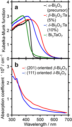
To determine the absorption characteristics of Bi-based samples, DR-UV-vis spectroscopy was used and compared with the simulated absorption coefficient as a function of wavelength. The results are shown in Fig. 7. The Kubelka–Munk functions of the representative ones (Fig. 7a) show that for the pure α-Bi2O3 precursor, the adsorption edge was 445 nm in the near UV region, whereas that of β-Bi2O3:Ta (5%) was 550 nm. The absorption edges of the δ-Bi2O3:Ta (10%) and Bi3TaO7 were 530 and 440 nm, respectively. The bandgap energy calculation yields values of 2.8, 2.2, 2.3, and 2.8 eV for α-Bi2O3, β-Bi2O3:Ta (5%), δ-Bi2O3:Ta (10%), and Bi3TaO7, respectively. The visible-light responsiveness of β-Bi2O3 and δ-Bi2O3 were simulated on our slab models whose structures were optimized without adding Ta. The simulated absorption spectra are shown in Fig. 7b, and their absorption edges nearly correspond to those of the experimental spectra. In general, the degree of absorption coefficient is considered low for these Bi2O3, compared to other general compound-based semiconductors.47
Because it remained possible that the visible-light responsiveness (2.2 eV bandgap) is derived from the existence of defects especially caused by added Ta in the β-Bi2O3:Ta (5%), photoluminescence spectroscopy was conducted. The results are shown in Fig. S6 (ESI†). For the α-Bi2O3 (precursor) shown in Fig. S6a (ESI†), the emission spectra triggered by 400 nm excitation light show a peak at 500–700 nm attributable to the existence of a defect level within the bandgap. However, the photoluminescence spectrum of our β-Bi2O3:Ta (5%) shown in Fig. S6b (ESI†) did not exhibit noticeable peaks other than a small peak at 560 nm attributed to near bandgap emission. This result does not contradict the statement that the photon absorption at band edges is mainly β-Bi2O3 bandgap excitation.
The band alignment of the CBM and the VBM positions of the synthesized samples was experimentally estimated by using PESA. The VBM potentials estimated by ionization potentials were obtained by the crossing point of the linear part of the curve with the background from PESA. The spectra of representative samples are shown in Fig. 8, and all other spectra of the Bi–Ta oxides are shown in Fig. S7 (ESI†). The VBMs do not shift significantly but remain constant at 6.4–6.6 eV vs. vacuum (i.e., 2.0–2.2 eV vs. SHE), as expected from the contribution of O 2p orbitals. The determined band positions are summarized in Fig. 9 together with the Ta/Bi ratio and the resulting crystal phase. The results suggest that the conduction band positions are largely altered while valence band positions are relatively consistent.
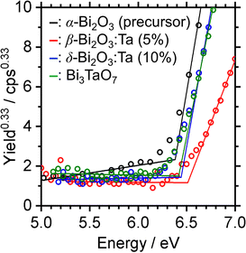 | ||
| Fig. 8 Photoelectron spectra in air (PESA) of α-Bi2O3 (precursor), β-Bi2O3:Ta (5%), δ-Bi2O3:Ta (10%), and Bi3TaO7. | ||
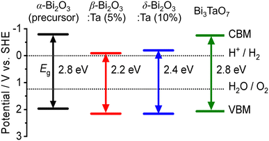 | ||
| Fig. 9 The experimental band positions of α-Bi2O3 (precursor), β-Bi2O3:Ta (5%), δ-Bi2O3:Ta (10%), and Bi3TaO7. The bandgap (Eg) and valence band maximum (VBM) of each sample were determined by DR-UV-vis spectroscopy (Fig. 7a) and photoelectron spectroscopy in air (PESA) (Fig. 8), respectively. | ||
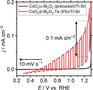
To check the photoresponsive behavior of α-Bi2O3 (precursor) and β-Bi2O3:Ta (5%), LSV (linear sweep voltammetry) under chopped-light illumination was conducted for CoOx/α-Bi2O3 (precursor)/Ti–Sn, and CoOx/β-Bi2O3:Ta (5%)/Ti–Sn particle–transferred electrodes. The result is shown in Fig. 10. The CoOx/α-Bi2O3 (precursor)/Ti–Sn electrode did not exhibit a pronounced response to the light, but the CoOx/β-Bi2O3:Ta (5%)/Ti–Sn electrode showed a pronounced anodic photocurrent. Because the Xe-lamp was used with a cut-off filter as the light source (420 < λ < 650 nm), this spectrum indicates that this material can utilize visible light to produce photo-excited holes and electrons. The onset potential of the sacrificial reagent oxidation reaction was found to be 0.5 V vs. RHE under light illumination, despite the fact that it was 1.0 V vs. RHE under dark conditions. The anodic photocurrent of 0.1 mA cm−2 was found to be 1.25 V vs. RHE.
To determine the dielectric properties of β-Bi2O3:Ta (5%) and δ-Bi2O3:Ta (10%), we computed their dielectric constants and effective masses. In a dielectric material, the static dielectric constant (εr) has contributions from two factors: the electron density (ε∞) and the ion vibrations (εvib). The dielectric constants and effective masses are listed in Table 3, and the real and imaginary parts of the dielectric functions obtained using HSE06 and SOC are shown in Fig. S8 (ESI†). With these calculations, the charge carriers were found to be heavy, indicating poor photocatalytic properties.
Thermal redox properties
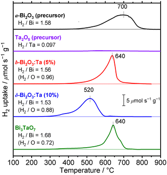
To investigate the difference of reducibility of our Bi-based oxides and consider an application for them as a material that is accompanied by thermal redox, TPR measurements were performed. The TPR profiles of the studied Bi–Ta oxides are shown in Fig. 11. A broad reduction peak of α-Bi2O3 (precursor) appeared at 700 °C. The atomic ratio of consumed H2 to Bi contained in the sample (H2/Bi ratio, Fig. 11) was calculated to be 1.58, and the total hydrogen consumption accounted for the complete reduction of the α-Bi2O3 (precursor) sample. The broadness of the peak can be attributed to the relatively large sizes of the α-Bi2O3 (precursor) particles, as seen in the SEM images (Fig. S3, ESI†). The peak was tailed to 400 °C, suggesting a faster reduction of the surface. TPR was also performed on the Ta2O5 (precursor), but substantial reduction was not observed throughout this temperature range up to 900 °C. β-Bi2O3:Ta (5%) showed reduction starting at around 400 °C, with a maximum at 640 °C, indicating facilitated reduction compared to α-Bi2O3 (precursor). Both the H2/Bi and H2/O ratios of 1.56 and 0.96 indicated the complete reduction of Bi atoms. δ-Bi2O3:Ta (10%) had a reduction peak starting at 300 °C, a markedly low temperature, with a maximum at 520 °C, again the lowest temperature among the samples investigated. These findings suggest that reduction of both bulk and the surface of δ-Bi2O3:Ta (10%) was easiest among the samples. This facilitated redox property might be explained by the high mobility of oxygen species related to the low occupancy of O sites due to its defective crystal structure. The consumption of hydrogen (H2/Bi = 1.53 and H2/O = 0.88) can be explained if it is assumed that the Ta atoms are not reduced, and that only Bi atoms are reduced, as expressed by the following reaction (note that δ-Bi2O3:Ta [10%] is expressed as Bi2Ta0.2O3.5):| Bi2Ta0.2O3.5 + 3H2 → 2Bi + 3H2O + 0.1Ta2O5 | (1) |
| (H2/Bi = 3/2 = 1.5, H2/O = 3/3.5 = 0.857) |
| Bi3TaO7 + 4.5H2 → 3Bi + 4.5H2O + 0.5Ta2O5 | (2) |
| (H2/Bi = 4.5/3 = 1.5, H2/O = 4.5/7 = 0.643) |
| Among these oxides, δ-Bi2O3:Ta (10%) appeared to have a TPR peak at the lowest temperature, meaning the highest thermal redox properties. This material is expected to be utilized as a catalyst or its support for reactions that are accompanied by oxidation or reduction. Further investigations into the applications of this material as a thermal catalyst or its support are expected. |
Conclusions
In summary, this investigation of the Ta-supplemented bismuth oxides, such as α-Bi2O3, β-Bi2O3, δ-Bi2O3 and Bi3TaO7, confirms that the crystal structures and optoelectronic properties of these oxides are altered according to the amount of added Ta (as Ta2O5). Heat treatment at 850 °C and cooling of Bi2O3 with different amounts of added Ta controllably led to the formation of α-Bi2O3, β-Bi2O3, and δ-Bi2O3. Among them, β-Bi2O3 was found to be a promising visible-light harvesting material, as it has the narrowest bandgap of 2.2 eV. DFT calculations using the HSE exchange–correlation functional and PESA measurements demonstrate that the conduction band has a large contribution from Bi orbitals in β-Bi2O3 and δ-Bi2O3. We confirmed that the presence of added Ta is not essential to alter the band structures of bismuth oxides by causing a defect level but, rather, by changing the crystal phase of bismuth oxides. However, the DFT calculations also suggested that β-Bi2O3 and δ-Bi2O3, which have bandgaps narrow enough to absorb visible light, are limited in their applicability as a photocatalyst due to their large effective masses and resultant low charge mobilities. In addition, different Bi2O3 polymorphs exhibited distinctive reducibility upon hydrogen treatment at high temperatures, showing that δ-Bi2O3 was reduced at the lowest temperature among the samples investigated. The wide range of methodologies adopted in this study and the knowledge gained into the semiconductor structure of a mixed oxide through these methodologies will allow us to identify and understand other novel candidate materials for applications such as photocatalysis and thermal catalysis.Author contributions
All authors contributed to writing the manuscript. All authors approved the final version of the manuscript.Conflicts of interest
There are no conflicts to declare.Acknowledgements
This work was supported by the Mohammed bin Salman Center for Future Science and Technology for Saudi-Japan Vision 2030 at the University of Tokyo (MbSC2030). LC and RA acknowledge Shaheen and HPC Core Labs team at KAUST.Notes and references
- J. S. Ahn, M. A. Camaratta, D. Pergolesi, K. T. Lee, H. Yoon, B. W. Lee, D. W. Jung, E. Traversa and E. D. Wachsman, J. Electrochem. Soc., 2010, 157, B376 CrossRef
.
- R. D. Bayliss, S. N. Cook, S. Kotsantonis, R. J. Chater and J. A. Kilner, Adv. Energy Mater., 2014, 4, 1301575 CrossRef
.
- X. Kuang, J. L. Payne, M. R. Johnson and I. Radosavljevic Evans, Angew. Chem., Int. Ed., 2012, 51, 690–694 CrossRef CAS PubMed
.
- R. Punn, A. M. Feteira, D. C. Sinclair and C. Greaves, J. Am. Chem. Soc., 2006, 128, 15386–15387 CrossRef CAS
.
- K. Firman, K. B. Tan, C. C. Khaw, Z. Zainal, Y. P. Tan and S. K. Chen, J. Mater. Sci., 2017, 52, 10106–10118 CrossRef CAS
.
- M. Gambino, F. Giannici, A. Longo, S. Di Tommaso, F. Labat and A. Martorana, J. Phys. Chem. C, 2015, 119, 26367–26373 CrossRef
.
- R. Oka, Y. Shobu and T. Masui, ACS Omega, 2019, 4, 7581–7585 CrossRef PubMed
.
- M. Li, F. Li and P. G. Yin, Chem. Phys. Lett., 2014, 601, 92–97 CrossRef
.
- S. J. A. Moniz, D. Bhachu, C. S. Blackman, A. J. Cross, S. Elouali, D. Pugh, R. Q. Cabrera and S. Vallejos, Inorg. Chim. Acta, 2012, 380, 328–335 CrossRef
.
- M. Schlesinger, S. Schulze, M. Hietschold and M. Mehring, Dalton Trans., 2013, 42, 1047–1056 RSC
.
- Y. Lu, Y. Zhao, J. Zhao, Y. Song, Z. Huang, F. Gao, N. Li and Y. Li, Cryst. Growth Des., 2015, 15, 1031–1042 CrossRef CAS
.
- L. Zhang, Y. Shi, Z. Wang, C. Hu, B. Shi and X. Cao, Appl. Catal., B, 2020, 265, 118563 CrossRef CAS
.
- S. Singh and R. Sharma, Sol. Energy Mater. Sol. Cells, 2018, 186, 208–216 CrossRef CAS
.
- Y. C. Wu, Y. C. Chaing, C. Y. Huang, S. F. Wang and H. Y. Yang, Dyes Pigm., 2013, 98, 25–30 CrossRef CAS
.
- S. Zhong, S. Zou, X. Peng, J. Ma and F. Zhang, J. Sol-Gel Sci. Technol., 2015, 74, 220–226 CrossRef
.
- H. Sudrajat, J. Nanopart. Res., 2017, 19, 1–8 CrossRef
.
- J. C. Medina, M. Bizarro, P. Silva-Bermudez, M. Giorcelli, A. Tagliaferro and S. E. Rodil, Thin Solid Films, 2016, 612, 72–81 CrossRef
.
- H. Sudrajat and P. Sujaridworakun, Mater. Des., 2017, 130, 501–511 CrossRef
.
- S. Zhu, L. Lu, Z. Zhao, T. Wang, X. Liu, H. Zhang, F. Dong and Y. Zhang, J. Phys. Chem. C, 2017, 121, 9394–9401 CrossRef
.
- H. Sudrajat and S. Hartuti, Adv. Powder Technol., 2019, 30, 983–991 CrossRef
.
- S. J. A. Moniz, C. S. Blackman, C. J. Carmalt and G. Hyett, J. Mater. Chem., 2010, 20, 7881–7886 RSC
.
- G. D. Lim, J. H. Yoo, M. Ji and Y. I. Lee, J. Alloys Compd., 2019, 806, 1060–1067 CrossRef
.
- C. Chang, H.-C. Yang, N. Gao and S.-Y. Lu, J. Alloys Compd., 2018, 738, 138–144 CrossRef
.
- N. R. Khalid, Z. Israr, M. B. Tahir and T. Iqbal, Int. J. Hydrogen Energy, 2020, 45, 8479–8489 CrossRef
.
- Y. Shi, L. Luo, Y. Zhang, Y. Chen, S. Wang, L. Li, Y. Long and F. Jiang, Ceram. Int., 2017, 43, 7627–7635 CrossRef
.
- H. Sudrajat, Superlattices Microstruct., 2017, 109, 229–239 CrossRef
.
- A. H. Zahid and Q. Han, Nanoscale, 2021, 13, 17687–17724 RSC
.
- G. Guenther and O. Guillon, J. Mater. Res., 2014, 29, 1383–1392 CrossRef
.
- J. Wind, J. Polt, Z. Zhang, D. A. Blom, T. Vogt, R. L. Withers and C. D. Ling, Chem. Mater., 2017, 29, 9171–9181 CrossRef
.
- V. Fruth, A. Ianculescu, D. Berger, S. Preda, G. Voicu, E. Tenea and M. Popa, J. Eur. Ceram. Soc., 2006, 26, 3011–3016 CrossRef
.
- H. N. Lin, M. S. Chen, Y. H. Chang, P. Y. Lee and C. K. Lin, Materials, 2019, 12(12), 1947 CrossRef
.
- J. L. Ortiz-Quinonez, I. Zumeta-Dubé, D. Díaz, N. Nava-Etzana, E. Cruz-Zaragoza and P. Santiago-Jacinto, Inorg. Chem., 2017, 56, 3394–3403 CrossRef PubMed
.
- J. A. H. Dreyer, S. Pokhrel, J. Birkenstock, M. G. Hevia, M. Schowalter, A. Rosenauer, A. Urakawa, W. Y. Teoh and L. Mädler, CrystEngComm, 2016, 18, 2046–2056 RSC
.
- W. Humphrey, A. Dalke and K. Schulten, J. Mol. Graphics, 1996, 14, 33–38 CrossRef PubMed
.
- W. M. H. Sachtler, G. J. H. Dorgelo and A. A. Holscher, Surf. Sci., 1966, 5, 221–229 CrossRef
.
- G. Kresse and J. Hafner, Phys. Rev. B: Condens. Matter Mater. Phys., 1993, 48, 13115–13118 CrossRef
.
- G. Kresse and J. Furthmüller, Phys. Rev. B: Condens. Matter Mater. Phys., 1996, 54, 11169–11186 CrossRef
.
- P. E. Blöchl, Phys. Rev. B: Condens. Matter Mater. Phys., 1994, 50, 17953–17979 CrossRef
.
- H. J. Monkhorst and J. D. Pack, Phys. Rev. B: Solid State, 1976, 13, 5188–5192 CrossRef
.
- J. P. Perdew and Y. Wang, Phys. Rev. B: Condens. Matter Mater. Phys., 1992, 45, 13244–13249 CrossRef PubMed
.
- J. Heyd and G. E. Scuseria, J. Chem. Phys., 2004, 121, 1187–1192 CrossRef PubMed
.
- J. E. Peralta, J. Heyd, G. E. Scuseria and R. L. Martin, Phys. Rev. B: Condens. Matter Mater. Phys., 2006, 74, 073101 CrossRef
.
- M. Gmitra, S. Konschuh, C. Ertler, C. Ambrosch-Draxl and J. Fabian, Phys. Rev. B: Condens. Matter Mater. Phys., 2009, 80, 235431 CrossRef
.
- S. Yamazoe, Y. Hitomi, T. Shishido and T. Tanaka, J. Phys. Chem. C, 2008, 112, 6869–6879 CrossRef
.
- M. A. Laguna-Marco, C. Piquer, A. G. Roca, R. Boada, M. Andrés-Vergés, S. Veintemillas-Verdaguer, C. J. Serna, A. Iadecola and J. Chaboy, Phys. Chem. Chem. Phys., 2014, 16, 18301–18310 RSC
.
- J. Ribeiro, G. Tremiliosi-Filho, P. Olivi and A. R. Andrade, Mater. Chem. Phys., 2011, 125, 449–460 CrossRef CAS
.
-
O. Madelung, Semiconductors: Data Handbook, Springer, Berlin Heidelberg, 2012 Search PubMed
.
-
S. Adachi, GaAs and Related Materials: Bulk Semiconducting and Super-lattice Properties, World Scientific, 1994 Search PubMed
.
- T. Le Bahers, M. Rérat and P. Sautet, J. Phys. Chem. C, 2014, 118, 5997–6008 CrossRef
.
- S. Lardhi, D. Noureldine, M. Harb, A. Ziani, L. Cavallo and K. Takanabe, J. Chem. Phys., 2016, 144, 134702 CrossRef
.
- D. Noureldine, S. Lardhi, A. Ziani, M. Harb, L. Cavallo and K. Takanabe, J. Mater. Chem. C, 2015, 3, 12032–12039 RSC
.
Footnotes |
| † Electronic supplementary information (ESI) available. See DOI: https://doi.org/10.1039/d2tc03718a |
| ‡ These authors contributed equally. |
| This journal is © The Royal Society of Chemistry 2022 |

