
 Open Access Article
 This Open Access Article is licensed under a
 Creative Commons Attribution 3.0 Unported Licence
Tunability of topological edge states in germanene at room temperature
Dennis J.
Klaassen
 ,
Ilias
Boutis
,
Carolien
Castenmiller
and
Pantelis
Bampoulis
*
,
Ilias
Boutis
,
Carolien
Castenmiller
and
Pantelis
Bampoulis
*
Physics of Interfaces and Nanomaterials, MESA+ Institute, University of Twente, P.O. Box 217, 7500AE Enschede, The Netherlands. E-mail: p.bampoulis@utwente.nl
First published on 27th August 2024
Abstract
Germanene is a two-dimensional topological insulator with a large topological band gap. For its use in low-energy electronics, such as topological field effect transistors and interconnects, it is essential that its topological edge states remain intact at room temperature. In this study, we examine these properties in germanene using scanning tunneling microscopy and spectroscopy at 300 K and compare the results with data obtained at 77 K. Our findings show that the edge states persist at room temperature, although thermal effects cause smearing of the bulk band gap. Additionally, we demonstrate that, even at room temperature, applying an external perpendicular electric field switches the topological states of germanene off. These findings indicate that germanene's topological properties can be maintained and controlled at room temperature, making it a promising material for low-energy electronic applications.
Introduction
Two-dimensional topological insulators (2DTI) or quantum spin Hall insulators are atomically thin layers characterized by an energy gap in the bulk and two topologically protected gapless helical edge states. Kane and Mele showed that graphene is a 2DTI because of spin–orbit coupling (SOC).1,2 SOC induces an ‘effective’ magnetic field that pushes spin-up and spin-down electrons in opposite directions toward the material's edges. Time reversal symmetry prevents backscattering from non-magnetic impurities at these edge states, enabling dissipationless charge transport.3–8 However, due to graphene's small SOC-induced gap, observing the QSH effect in graphene requires extremely low temperatures (<0.1 K).9 The first practical demonstrations of the QSH effect were in semiconductor quantum wells such as HgTe/(Hg,Cd)Te6,10 and InAs/GaSb,11,12 and more recently also in other band-inverted ultra-thin materials,13–15 adhering to the Bernevig–Hughes–Zhang model.4 The challenge at hand is to make a 2DTI with a large band gap, significantly larger than kT, such that it still exhibits its topological properties at room temperature16–18 in order to harness their properties in device applications, such as topological interconnects, p–n junctions, and field-effect transistors.19 Large band gap mono elemental 2DTIs like bismuthene, stanene, and germanene were recently fabricated and could provide a solution to this challenge.15,20–33 Recently, topological states have been detected at high temperatures.34,35Germanene is an atomically thin layer of germanium atoms arranged in a buckled honeycomb lattice.23,36 Recently, we demonstrated that germanene is a 2DTI with a large enough topological band gap in the order of 70 meV.37 The buckled structure of germanene enables us to tune the band gap and the topological state of germanene by applying an electric field perpendicular to the germanene layer.37–42 This electric field-induced topological phase transition along with its relatively large band gap makes germanene a candidate for a room-temperature topological field effect transistor.42 In this letter, we check the suitability of germanene for room-temperature applications utilizing scanning tunneling microscopy and spectroscopy techniques to study the topological edge states of germanene at room temperature.
Methods
Scanning tunneling microscopy (STM) and scanning tunneling spectroscopy (STS) measurements are conducted using an ultrahigh vacuum low-temperature scanning tunneling microscope (Omicron LT-STM) operated at 77 K and 300 K using a PtIr tip or Au coated tip. PtIr is chosen for its stability and high conductivity. The tips were prepared by etching high-purity PtIr wire. The Au coating is achieved by doing STM measurements on an Au(111) substrate and gently dipping the tip into the substrate to ensure a thin coating. The background pressure in the ultrahigh vacuum STM chamber is below 3 × 10⁻¹¹ mbar. To grow germanene layers, 1.5 ± 0.5 monolayers of Pt are deposited on an atomically clean Ge(110) substrate. Subsequently, the Ge(110) sample is annealed for several minutes to a temperature of about 1100 K, which is above the eutectic temperature of the PtGe system (1047 K). Above the eutectic point, eutectic droplets are formed on top of the surface with a composition of Pt0.22Ge0.78. During the cooling process, the sample undergoes spinodal decomposition into a Ge2Pt phase and a pure Ge phase.24,43–47 During this process, the Ge2Pt clusters are decorated with several layers of germanene.24,37,48,49 Differential conductivity (dI(V)/dV), was measured at 77 K and room temperature using a lock-in amplifier. The frequency of the lock-in amplifier was set to 1.1–1.2 kHz and the modulation voltage was about 20 mV at 77 K and about 50 mV at room temperature. The spectroscopy data in this paper result from averaging tenths of individual dI(V)/dV curves. The line dI(V)/dV spectroscopy maps in this paper are plotted with a blue-white-red colormap which can be found in ref. 50.Results and discussion
Germanene has a buckled honeycomb structure consisting of two hexagonal sublattices, which are displaced with respect to each other in a direction normal to the germanene layer. In the top view of the ball and stick model of the germanene lattice in Fig. 1(a) the honeycomb structure is visible and the side view reveals the buckling effect. Fig. 1(b) shows a schematic of the band structure at the K and K′ points of the Brillouin zone of germanene with the edge states (blue and red) filling the bulk band gap. Similar to our earlier work,37,48 the first germanene layer (the buffer layer) couples to the underlying Ge2Pt(101) substrate causing the layer to be electronically dead. The top germanene layer is a two-dimensional topological insulator that host robust edge states as shown in the schematic of Fig. 1(b).37Fig. 1(c) shows a large-scale image of a typical Ge2Pt cluster covered with germanene layers including a step edge in the middle of the cluster. A high-resolution STM image on a typical germanene step edge can be seen in Fig. 2(d). Fig. 1(e) reveals a high-resolution STM image of the buckled honeycomb lattice of germanene acquired at room temperature with a lattice constant of (0.42 ± 0.02) nm. From Fig. 1(d) and (e) we can extract some other parameters of the buckled germanene lattice, i.e. the buckling and the step height. The graph in Fig. 1(f) shows the height profiles along the blue line in Fig. 1(d) and the green line in Fig. 1(e). From these, we extract a monoatomic step height of about 0.27 ± 0.02 nm, close to the expected 0.28 nm, and a buckling of ∼0.02–0.03 nm. We note here that STM images are influenced by both the topography and the local density of states (LDOS). Because of this, the exact value of the apparent buckling and the step height also depends on sample bias. This explains the slight differences in the measured step height and buckling compared to our previous work.37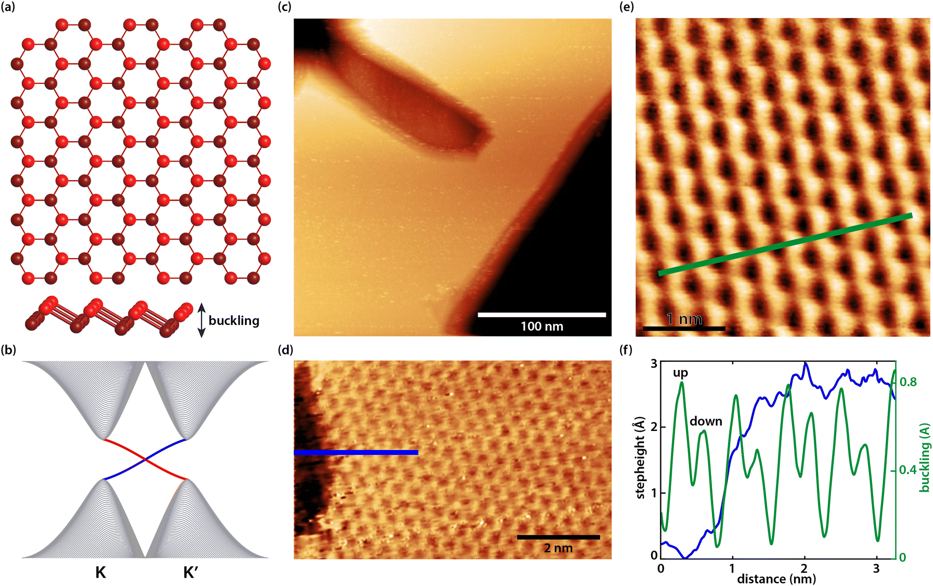 | ||
| Fig. 1 (a) Ball and stick model of the buckled honeycomb lattice of germanene (the bottom image is a side view that shows the buckling effect). (b) A schematic of the band structure of a 2DTI without an external electric field showing the bulk bands at the K and K′ points of the Brillouin zone (gray) and the edge states filling the bulk gap (blue and red). (c) Large-scale STM image of a Ge2Pt cluster covered with germanene. (d) High-resolution STM image on a germanene step edge. (e) Small-scale STM image of the buckled honeycomb lattice of germanene. (f) A graph showing the height profile across the step edge in (d) along the blue line, and a height profile along the green line in (e) revealing the buckling of the germanene lattice. | ||
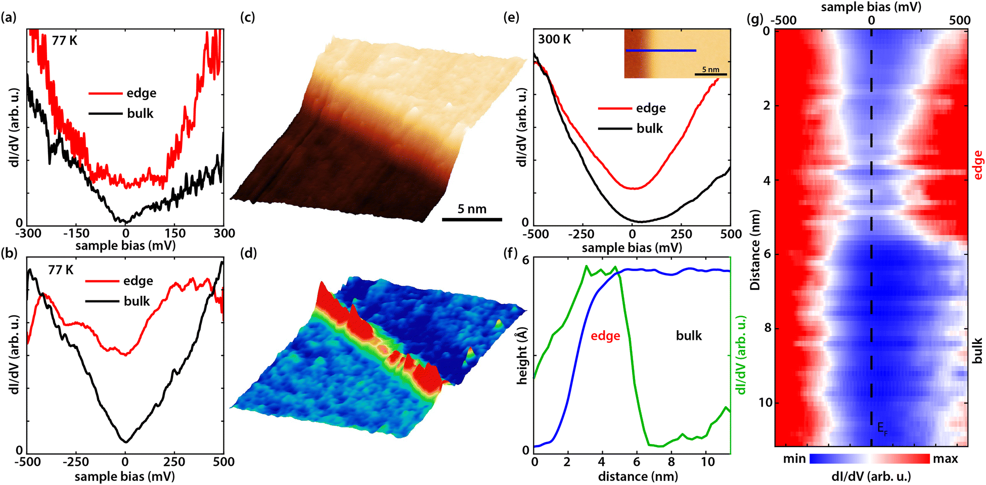 | ||
| Fig. 2 dI(V)/dV point spectra measured at 77 K on the edge and in the bulk of the germanene terrace with an external electric field of (a) ∼1.75 V nm−1 and (b) ∼1.95 V nm−1. (c) STM image of a germanene step edge and the corresponding dI(V)/dV map in (d) revealing the edge state (0.1 nA, 150 mV). (e) dI(V)/dV point spectrum measured at 300 K with an electric field of ∼1.80 V nm−1, on the edge and in the bulk of germanene shown in the inset. (f) Cross-sectional graph showing (blue) the height profile along the blue line in the inset of (e), and (green) the differential conductivity (dI(V)/dV) at the Fermi level (EF) along the same blue line. The step height is 0.54 ± 0.03 nm, corresponding to the height of two germanene layers. (g) Line dI(V)/dV spectroscopy perpendicular to the edge of the germanene terrace along the blue line in the inset of (e), the location of the edge and the bulk are indicated on the right. | ||
Fig. 2(a) and (b) show dI(V)/dV point spectra at 77 K at the edge and in the bulk of the germanene terrace at a tip-induced electric field of ∼1.75 V nm−1 and ∼ 1.95 V nm−1, respectively. In Fig. 2(a) an enhanced differential conductivity is visible at the edge compared to the bulk. Furthermore, the bulk dI(V)/dV curve indicates a band gap. Fig. 2(b) on the other hand reveals a V-shape semi-metallic signature in the bulk with an enhanced differential conductivity at the edges, which is expected for an electric field of ∼1.95 V nm−1 (ref. 37) as the tip-induced electric field closes the band gap. The V-shaped density of states (DOS) is one of the hallmarks of a 2D Dirac system. Fig. 2(c) shows a typical STM image on such a germanene edge. Fig. 2(d) shows the corresponding dI/dV map at the edge state energy revealing the pronounced metallic states at the germanene edge. On top of that, it illustrates that the edge state runs through the whole edge with small changes in intensity, possibly due to reconstructions or local change of termination.48 To check the stability of the edge states at room temperature we heated our cryostat to 300 K and repeated the experiments. Fig. 2(e) presents dI(V)/dV point spectra at 300 K at the edge and in the bulk of the germanene layer (shown in the inset) at an electric field of ∼1.80 V nm−1. The results in Fig. 2(e) show that the differential conductivity of the edge of the germanene layer is still significantly higher compared to the bulk. Note that the small gap or V-shape cannot be resolved due to thermal broadening of the spectra at room temperature.51 The full width at half maximum of the thermal broadening function is equal to 3.5kBT,48 which comes down to ∼90 meV at 300 K. On top of that, the instrumental broadening of the lock-in amplifier adds to the total convolution of the dI(V)/dV spectra. The full width at half maximum of the instrumental broadening function is given by 1.7Vm,48 where Vm is the modulation voltage. This means that we have an instrumental broadening term of ∼85 meV at 300 K (Vm = 50 meV). As a result, the total broadening at full width at half max, given by  , is ∼124 meV. Therefore, the combination of the thermal broadening and the instrumental broadening convolute the dI(V)/dV signal more than the size of the band gap (∼70 meV) of germanene for small electric fields,37 which makes it impossible to resolve the band gap. The blue curve in Fig. 2(f) represents the cross-sectional height profile across the germanene step edge along the blue line in the inset of Fig. 2(e). The height profile, reveals a step height of 0.54 ± 0.03 nm corresponding to about twice the monoatomic step height of germanene. The step height in the inset of Fig. 2(e) therefore translates to the height of two germanene layers on the buffer/Ge2Pt(101) substrate. The green curve in Fig. 2(f) reveals the dI(V)/dV cross-section at the Fermi level (EF) of the dI(V)/dV line spectroscopy measurement in Fig. 2(g), along the same blue line in the inset of Fig. 2(e). From these figures, it becomes clear that the metallic state is present up to room temperature, the edge state decays exponentially into the bulk with the decay length of about 2–3 nm.
Next, we test the effect of the tip-induced electric field on the edge states of germanene. As explained extensively in ref. 37 we apply a local electric field perpendicular to the germanene terrace using the difference in work function between the STM tip and the sample. The electric field can be estimated by Ez = (Φtip − Φgermanene)/ez, where Ez is the electric field, z the tip-sample distance, Φtip and Φgermanene the work function of the tip (ΦPtIr = 5.7 eV and ΦAu = 5.2 eV) and that of germanene (ΦGe = 4.0 eV (ref. 52)) respectively, and e the elementary charge.37,53 Changing the tip-sample separation distance will thus change the local perpendicular electric field. Similarly, we can change the electric field by coating the tip with another material with a different work function. We note here that this method is only an estimate; a systematic error of up to 50% may arise from inaccuracies in the tip-sample distance, work functions, image charges, and band bending,37 but does not change the qualitative picture. Increasing the electric field causes charge to shift from one sublattice to the other, breaking inversion symmetry. The band gap closes at a critical field (∼1.95 V nm−1) making it a topological semi-metal as demonstrated in our previous work.37 Above the critical electric field, the band gap reopens again, the topologically protected edge channels disappear, and the material becomes topologically trivial. With a perpendicular electric field, we can thus change the topological phase of germanene from a topological insulator to a topological semi-metal and then to a trivial band insulator. Fig. 3(a) and (d) present dI(V)/dV point spectra, obtained at room temperature, at the edge and in the bulk of the germanene layer at (a) an electric field below the critical field (∼1.80 V nm−1) and (d) at an electric field above the critical field (∼2.10 V nm−1). The corresponding dI(V)/dV line spectroscopy measurements are presented in Fig. 3(b) and (e), respectively. Fig. 3(c) and (f) reveal dI/dV maps on the germanene step edge for a low electric field (∼1.80 V nm−1) and a high electric field (∼2.10) V nm−1, respectively. The point spectra for an electric field of ∼1.80 V nm−1, show that the DOS at the edge is much higher than that at the bulk. The point spectra in Fig. 3(d) at an electric field above the critical electric field show that the state at the edge has disappeared and that the edge and bulk curve almost overlap. Increasing the electric field above the critical electric field (∼1.95 V nm−1) switches the edge states of germanene ‘off’ in line with earlier results at 77 K.37 For an electric field below the critical electric field, the dI(V)/dV line spectroscopy measurement in Fig. 3(b) shows that the metallic edge state is localized at the edge similar to earlier results in Fig. 2(f) and (g). In the dI(V)/dV line spectroscopy measurement for an electric field above the critical electric field, Fig. 3(e), the state at the edge is no longer present. The same can be seen in the dI/dV maps in Fig. 3(c) for an electric field of (∼1.80 V nm−1) and in Fig. 3(f) for an electric field of (∼2.10 V nm−1). Finally, to check the robustness and repeatability of this switching process, we repeated it multiple times. Fig. 4 reveals the results of this experiment. The black circles present the averaged and normalized dI/dV at the edge state energy at the germanene edge obtained during the repetitions for a tip-induced electric field of ∼1.85 V nm−1 where the metallic edge states are ‘on’ and for an electric field of ∼2.20 V nm−1 where the metallic edge states are ‘off’. The results show that the switching process of the topological edge channels by applying an external perpendicular electric field is reversible.
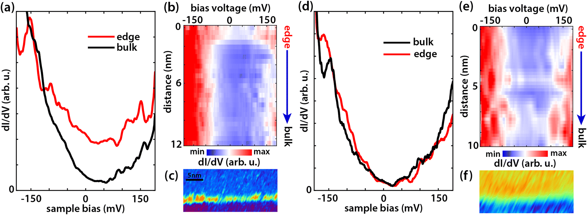 | ||
| Fig. 3 dI(V)/dV point spectra at the edge and in the bulk of the germanene terrace for (a) an electric field below the critical electric field (∼1.80 V nm−1) and (d) above the critical electric field (∼2.10 V nm−1) at room temperature (300 K). (a) Shows an increased differential conductivity at the edge compared to the bulk, while (d) does not. (b) and (e) Show line dI(V)/dV spectroscopy from the edge towards the bulk of the germanene terrace for (a) an electric field of (∼1.80 V nm−1) and (e) for (∼2.10 V nm−1). (c) and (f) Represent dI(V)/dV maps of the germanene step edge with setpoints (c) 0.1 nA, −0.1 V (∼1.80 V nm−1), and (f) 0.3 nA, −0.5V (∼2.10 V nm−1). (c) Shows a state along the step edge of the germanene terrace, while in (f) no state along the step edge can be resolved. | ||
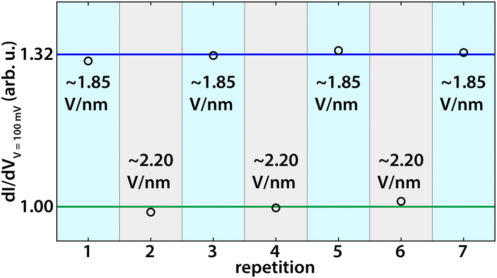 | ||
| Fig. 4 Averaged and normalized (to the 'off' state) dI/dV recorded at the edge state energy (100 mV) at the germanene step edge for varying tunnel currents/electric fields (black circles). The blue curve represents the average dI/dV for a tip-induced electric field of ∼1.85 V nm−1 when the topological edge state is ‘on.’ The green curve represents the average dI/dV for a tip-induced electric field of ∼ 2.20 V nm−1 when the topological edge state is ‘off’. | ||
Conclusions
In this study, we have demonstrated that the topological properties of germanene are preserved at room temperature. Using scanning tunneling microscopy and spectroscopy at 300 K, we observed robust metallic edge states in the germanene layer. Although thermal broadening at room temperature prevents us from resolving the band gap, the persistence of edge states confirms the stability of germanene's topological characteristics. This is further supported by the demonstration of the electric-field induced topological phase transition at room temperature, switching the germanene edge states on and off using an electric field. The ability to maintain and control its topological properties under ambient conditions makes germanene a promising candidate for next-generation electronic devices.19,42,54–57Data availability
Data for this article, including the description of the data are available at 4TU.ResearchData at doi.org/10.4121/6617eb98-b8a0-4676-ae94-1dbb7bb56e02.Conflicts of interest
There are no conflicts to declare.Acknowledgements
C. C., D. J. K. acknowledge NWO (Grants 16PR3237 and OCENW.M20.232) for financial support. P. B. acknowledges NWO Veni for financial support. D. J. K. and P. B. also acknowledge Professor H. J. W. Zandvliet for fruitful discussions.Notes and references
- C. L. Kane and E. J. Mele, Phys. Rev. Lett., 2005, 95, 146802 CrossRef CAS PubMed.
- C. L. Kane and E. J. Mele, Phys. Rev. Lett., 2005, 95, 226801 CrossRef CAS PubMed.
- M. Z. Hasan and C. L. Kane, Rev. Mod. Phys., 2010, 82, 3045–3067 CrossRef CAS.
- B. A. Bernevig, T. L. Hughes and S.-C. Zhang, Science, 2006, 314, 1757–1761 CrossRef CAS PubMed.
- B. A. Bernevig and S.-C. Zhang, Phys. Rev. Lett., 2006, 96, 106802 CrossRef PubMed.
- M. König, S. Wiedmann, C. Brüne, A. Roth, H. Buhmann, L. W. Molenkamp, X.-L. Qi and S.-C. Zhang, Science, 2007, 318, 766–770 CrossRef PubMed.
- C. Wu, B. A. Bernevig and S.-C. Zhang, Phys. Rev. Lett., 2006, 96, 106401 CrossRef PubMed.
- X.-L. Qi and S.-C. Zhang, Rev. Mod. Phys., 2011, 83, 1057–1110 CrossRef CAS.
- Y. Yao, F. Ye, X.-L. Qi, S.-C. Zhang and Z. Fang, Phys. Rev. B: Condens. Matter Mater. Phys., 2007, 75, 041401 CrossRef.
- A. Roth, C. Brüne, H. Buhmann, L. W. Molenkamp, J. Maciejko, X.-L. Qi and S.-C. Zhang, Science, 2009, 325, 294–297 CrossRef CAS PubMed.
- I. Knez, R.-R. Du and G. Sullivan, Phys. Rev. Lett., 2011, 107, 136603 CrossRef PubMed.
- T. Li, P. Wang, H. Fu, L. Du, K. A. Schreiber, X. Mu, X. Liu, G. Sullivan, G. A. Csáthy, X. Lin and R.-R. Du, Phys. Rev. Lett., 2015, 115, 136804 CrossRef PubMed.
- Z. Fei, T. Palomaki, S. Wu, W. Zhao, X. Cai, B. Sun, P. Nguyen, J. Finney, X. Xu and D. H. Cobden, Nat. Phys., 2017, 13, 677–682 Search PubMed.
- S. Tang, C. Zhang, D. Wong, Z. Pedramrazi, H.-Z. Tsai, C. Jia, B. Moritz, M. Claassen, H. Ryu, S. Kahn, J. Jiang, H. Yan, M. Hashimoto, D. Lu, R. G. Moore, C.-C. Hwang, C. Hwang, Z. Hussain, Y. Chen, M. M. Ugeda, Z. Liu, X. Xie, T. P. Devereaux, M. F. Crommie, S.-K. Mo and Z.-X. Shen, Nat. Phys., 2017, 13, 683–687 Search PubMed.
- F. Reis, G. Li, L. Dudy, M. Bauernfeind, S. Glass, W. Hanke, R. Thomale, J. Schäfer and R. Claessen, Science, 2017, 357, 287–290 CrossRef CAS PubMed.
- Y. Xu, B. Yan, H.-J. Zhang, J. Wang, G. Xu, P. Tang, W. Duan and S.-C. Zhang, Phys. Rev. Lett., 2013, 111, 136804 CrossRef PubMed.
- C. Niu, H. Wang, N. Mao, B. Huang, Y. Mokrousov and Y. Dai, Phys. Rev. Lett., 2020, 124, 066401 CrossRef CAS PubMed.
- Y. Bai, L. Cai, N. Mao, R. Li, Y. Dai, B. Huang and C. Niu, Phys. Rev. B, 2022, 105, 195142 CrossRef CAS.
- M. J. Gilbert, Commun. Phys., 2021, 4, 70 CrossRef CAS.
- N. R. Glavin, R. Rao, V. Varshney, E. Bianco, A. Apte, A. Roy, E. Ringe and P. M. Ajayan, Adv. Mater., 2020, 32, 1904302 CrossRef CAS PubMed.
- F. Matusalem, M. Marques, L. K. Teles, L. Matthes, J. Furthmüller and F. Bechstedt, Phys. Rev. B, 2019, 100, 245430 CrossRef CAS.
- E. Bianco, S. Butler, S. Jiang, O. D. Restrepo, W. Windl and J. E. Goldberger, ACS Nano, 2013, 7, 4414–4421 CrossRef CAS PubMed.
- A. Acun, L. Zhang, P. Bampoulis, M. Farmanbar, A. van Houselt, A. N. Rudenko, M. Lingenfelder, G. Brocks, B. Poelsema, M. I. Katsnelson and H. J. W. Zandvliet, J. Phys.: Condens. Matter, 2015, 27, 443002 CrossRef CAS PubMed.
- P. Bampoulis, L. Zhang, A. Safaei, R. van Gastel, B. Poelsema and H. J. W. Zandvliet, J. Phys.: Condens. Matter, 2014, 26, 442001 CrossRef CAS PubMed.
- L. Zhang, P. Bampoulis, A. N. Rudenko, Q. Yao, A. Van Houselt, B. Poelsema, M. I. Katsnelson and H. J. W. Zandvliet, Phys. Rev. Lett., 2016, 116, 256804 CrossRef CAS PubMed.
- H. J. W. Zandvliet, Xenes, Elsevier, 2022, pp. 27–48 Search PubMed.
- T. Hu, X. Hui, X. Zhang, X. Liu, D. Ma, R. Wei, K. Xu and F. Ma, J. Phys. Chem. Lett., 2018, 9, 5679–5684 CrossRef CAS PubMed.
- Z. Yang, Z. Wu, Y. Lyu and J. Hao, InfoMat, 2019, 1, 98–107 CrossRef CAS.
- H. Zhao, S. Guo, W. Zhong, S. Zhang, L. Tao and H. Zeng, Xenes, Elsevier, 2022, pp. 173–196 Search PubMed.
- A. Zhao, Xenes, Elsevier, 2022, pp. 49–72 Search PubMed.
- F. F. Zhu, W. J. Chen, Y. Xu, C. L. Gao, D. D. Guan, C. H. Liu, D. Qian, S. C. Zhang and J. F. Jia, Nat. Mater., 2015, 14, 1020–1025 CrossRef CAS PubMed.
- J. Deng, B. Xia, X. Ma, H. Chen, H. Shan, X. Zhai, B. Li, A. Zhao, Y. Xu, W. Duan, S. C. Zhang, B. Wang and J. G. Hou, Nat. Mater., 2018, 17, 1081–1086 CrossRef CAS PubMed.
- F. Bechstedt, P. Gori and O. Pulci, Prog. Surf. Sci., 2021, 96, 100615 CrossRef CAS.
- S. Wu, V. Fatemi, Q. D. Gibson, K. Watanabe, T. Taniguchi, R. J. Cava and P. Jarillo-Herrero, Science, 2018, 359, 76–79 CrossRef CAS PubMed.
- N. Shumiya, M. S. Hossain, J.-X. Yin, Z. Wang, M. Litskevich, C. Yoon, Y. Li, Y. Yang, Y.-X. Jiang, G. Cheng, Y.-C. Lin, Q. Zhang, Z.-J. Cheng, T. A. Cochran, D. Multer, X. P. Yang, B. Casas, T.-R. Chang, T. Neupert, Z. Yuan, S. Jia, H. Lin, N. Yao, L. Balicas, F. Zhang, Y. Yao and M. Z. Hasan, Nat. Mater., 2022, 21, 1111–1115 CrossRef CAS PubMed.
- S. Cahangirov, M. Topsakal, E. Aktürk, H. Sahin and S. Ciraci, Phys. Rev. Lett., 2009, 102, 236804 CrossRef CAS PubMed.
- P. Bampoulis, C. Castenmiller, D. J. Klaassen, J. van Mil, Y. Liu, C.-C. Liu, Y. Yao, M. Ezawa, A. N. Rudenko and H. J. W. Zandvliet, Phys. Rev. Lett., 2023, 130, 196401 CrossRef CAS PubMed.
- M. Ezawa, New J. Phys., 2012, 14, 033003 CrossRef.
- M. Ezawa, J. Phys. Soc. Jpn., 2015, 84, 121003 CrossRef.
- L. Matthes and F. Bechstedt, Phys. Rev. B: Condens. Matter Mater. Phys., 2014, 90, 165431 CrossRef.
- W. G. Vandenberghe and M. V. Fischetti, Nat. Commun., 2017, 8, 14184 CrossRef CAS PubMed.
- X. Qian, J. Liu, L. Fu and J. Li, Science, 2014, 346, 1344–1347 CrossRef CAS PubMed.
- Z. Zhang, B. Poelsema, H. J. W. Zandvliet and A. van Houselt, J. Phys. Chem. C, 2022, 126, 11285–11297 CrossRef CAS PubMed.
- B. Poelsema, Z. Zhang, J. S. Solomon, H. J. W. Zandvliet and A. van Houselt, Phys. Rev. Mater., 2021, 5, 125602 CrossRef CAS.
- Z. Zhang, B. Poelsema, H. J. W. Zandvliet and A. van Houselt, Phys. Rev. Mater., 2021, 5, 105601 CrossRef CAS.
- B. Poelsema, Z. Zhang, H. J. W. Zandvliet and A. van Houselt, Phys. Rev. Lett., 2023, 131, 106201 CrossRef CAS PubMed.
- R. van Bremen, P. Bampoulis, J. Aprojanz, M. Smithers, B. Poelsema, C. Tegenkamp and H. J. W. Zandvliet, J. Appl. Phys., 2018, 124, 125301 CrossRef.
- H. J. W. Zandvliet, D. J. Klaassen and P. Bampoulis, Phys. Rev. B, 2024, 109, 115419 CrossRef CAS.
- P. Bampoulis, C. Castenmiller, D. J. Klaassen, J. van Mil, P. L. de Boeij, M. Ezawa and H. J. W. Zandvliet, 2D Mater., 2024, 11, 035016 CrossRef.
- A. Auton, Red Blue Colormap, 2024, https://www.mathworks.com/matlabcentral/fileexchange/25536-red-blue-colormap Search PubMed.
- C. J. Walhout, A. Acun, L. Zhang, M. Ezawa and H. J. W. Zandvliet, J. Phys.: Condens. Matter, 2016, 28, 284006 CrossRef CAS PubMed.
- B. Borca, C. Castenmiller, M. Tsvetanova, K. Sotthewes, A. N. Rudenko and H. J. W. Zandvliet, 2D Mater., 2020, 7, 035021 CrossRef CAS.
- J. L. Collins, A. Tadich, W. Wu, L. C. Gomes, J. N. B. Rodrigues, C. Liu, J. Hellerstedt, H. Ryu, S. Tang, S.-K. Mo, S. Adam, S. A. Yang, M. S. Fuhrer and M. T. Edmonds, Nature, 2018, 564, 390–394 CrossRef CAS PubMed.
- M. S. Lodge, S. A. Yang, S. Mukherjee and B. Weber, Adv. Mater., 2021, 33, 2008029 CrossRef CAS.
- W. Han, Y. Otani and S. Maekawa, npj Quantum Mater., 2018, 3, 27 CrossRef.
- Y. Ren, Z. Qiao and Q. Niu, Rep. Prog. Phys., 2016, 79, 066501 CrossRef PubMed.
- A. Molle, J. Goldberger, M. Houssa, Y. Xu, S.-C. Zhang and D. Akinwande, Nat. Mater., 2017, 16, 163–169 CrossRef CAS PubMed.
| This journal is © The Royal Society of Chemistry 2024 |