DOI:
10.1039/D4NH00030G
(Review Article)
Nanoscale Horiz., 2024, Advance Article
Innovations of metallic contacts on semiconducting 2D transition metal dichalcogenides toward advanced 3D-structured field-effect transistors
Received
19th January 2024
, Accepted 17th June 2024
First published on 8th July 2024
Abstract
2D semiconductors, represented by transition metal dichalcogenides (TMDs), have the potential to be alternative channel materials for advanced 3D field-effect transistors, such as gate-all-around field-effect-transistors (GAAFETs) and complementary field-effect-transistors (C-FETs), due to their inherent atomic thinness, moderate mobility, and short scaling lengths. However, 2D semiconductors encounter several technological challenges, especially the high contact resistance issue between 2D semiconductors and metals. This review provides a comprehensive overview of the high contact resistance issue in 2D semiconductors, including its physical background and the efforts to address it, with respect to their applicability to GAAFET structures.
1. Introduction
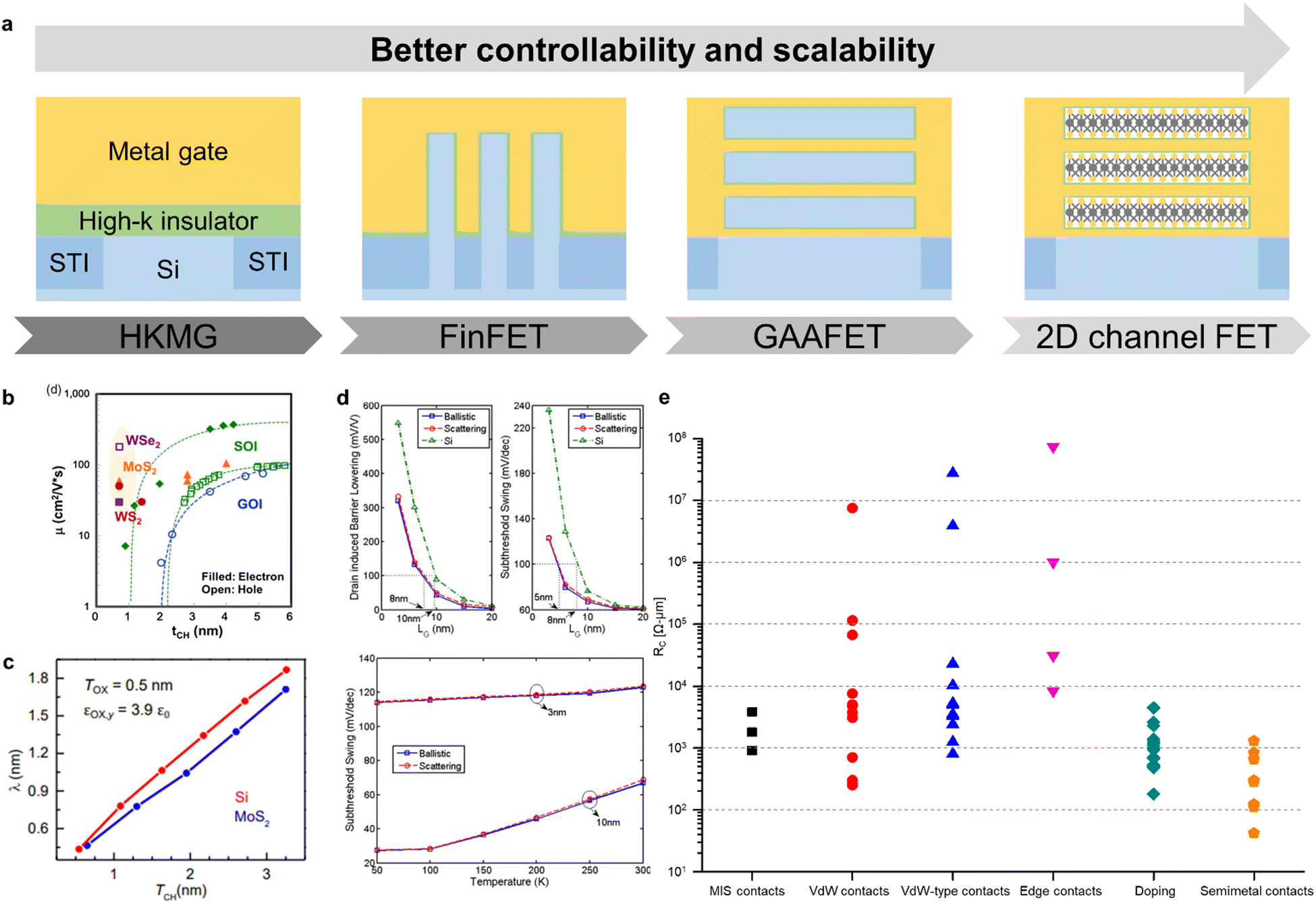
The electronics industry has been further developed through the miniaturization of transistors in integrated circuits, providing enhanced performance and greater energy efficiency in computing power.1 The continuous progression toward smaller transistor size has been enabled through the introduction of innovative materials like high-k metal gate (HKMG)2 and novel transistor designs such as fin field-effect transistors (FinFETs).3 Recently, gate-all-around field-effect transistors (GAAFETs) have emerged as a subsequent device architecture to FinFETs, with the potential to propel technological node advancements further (Fig. 1(a)).4 GAAFETs deliver enhanced performance and scalability when compared to FinFETs or conventional metal-oxide-semiconductor field-effect transistors (MOSFETs). The structure of GAAFET involves its channel surrounded by a gate on all sides, providing improved electrostatic control, faster switching speed and lower power consumption. Furthermore, it provides advanced scalability because its channels can be stacked vertically.4–6 This could also be applicable to the fabrication of complementary FETs (CFETs), in which n- and p-type MOSFETs are stacked on top of each other.7 Thus, GAAFET technology has been actively researched and developed by semiconductor manufacturers as a successor to FinFET technology.8
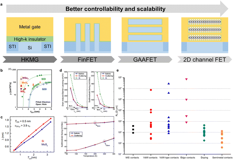 |
| | Fig. 1 (a) Schematics of a planar MOSFET with HKMG, FinFET, GAAFET, and 2D channel FET. (b) Carrier mobility versus thickness of WSe2, MoS2, WS2, silicon (Si), and germanium (Ge). Filled symbols refer to electron mobilities and open symbols to hole mobilities. The mobilities of 2D semiconductors show moderate values at sub-1 nm thickness, while those of silicon and germanium drastically decrease. Reprinted from ref. 9 with permission from John Wiley and Sons. (c) Scaling length versus channel thickness of MoS2 and Si. MoS2 shows a smaller scaling length, indicating better immunity to short channel effects (SCEs). Reprinted from ref. 10 with permission from The American Association for the Advancement of Science. (d) Drain-induced barrier lowering (DIBL) and subthreshold swing (SS) versus gate lengths of Si channel FETs (green) and MoS channel FETs (red and blue), SS versus temperature of MoS2 channel FETs. MoS2 shows lower DIBL and SS. Reprinted from ref. 11 with permission from IEEE. (e) Comparison of reported contact resistance values versus various contact engineering technologies. The data are from ref. 12–71. | |
Further downscaling of GAAFETs toward advanced technological nodes is anticipated to accompany the thinning of their channels.72,73 However, the utilization of silicon (Si) as a channel material for GAAFETs encounters a limitation in reducing the channel thickness to less than 5 nm, primarily because it results in substantial mobility degradation.74,75 Consequently, researchers have initiated investigations into 2D semiconductors, represented by transition metal dichalcogenides (TMDs),76 as a prospective substitute channel material for GAAFETs. In contrast to silicon, 2D semiconductors exhibit a reasonable carrier mobility, even if their thickness is less than 1 nm, due to their inherent atomic thinness and dangling-bond-free nature (Fig. 1(b)).9 They also have a notably lower dielectric constant compared to that of silicon, exhibiting a significantly reduced scaling length that indicates enhanced immunity to short-channel effects (Fig. 1(c) and (d)).10,11
Despite the advantages offered by 2D semiconductors, integrating them into the channel region is challenging due to the stringent requirements of a stable and matured process technology compatible with logic device technology reliant on a 300 mm wafer fabrication process. The technological hurdles that 2D semiconductors face include wafer-scale single-crystalline growth and high-quality HKMG stack formation.
Notably, the presence of high contact resistance at the metal/2D semiconductor junction emerges as a significant issue. Despite the dangling-bond-free nature of 2D semiconductors, the occurrence of Fermi-level pinning (FLP) phenomena77 at these junctions leads to a substantial injection barrier height for both electrons and holes. Moreover, there is a van der Waals (vdW) gap present between the metal and 2D semiconductors, serving as a tunnelling barrier.78 As a result, the substantial barrier height and the vdW gap impede the injection of carriers from the metal to 2D semiconductors and vice versa. This results in elevated contact resistance, typically ranging from a few to several tens of kΩ μm for multilayer 2D semiconductors. The contact resistance in monolayer 2D semiconductors experiences an increase due to their larger bandgap when compared to their bulk counterparts,76 reaching values up to several hundreds of kΩ μm.79 Furthermore, addressing the challenge of high contact resistance becomes even more formidable in advanced technological nodes, where contacts must be established in intricate and limited 3D spaces. This limitation can constrain choices for contact engineering strategies. The elevated contact resistance begins to impede the on-current, even in relatively long-channel 2D FETs (LCH = 1 μm).80 Scaled 2D channel FETs with reduced channel lengths (LCH < 1 μm) typically exhibit an on-current in the range of a few hundred μA μm−1 without the application of contact engineering technologies,81,82 which needs to be improved to meet the range of 532–753 μA μm−1 required for future technology nodes.83 Achieving this range is imperative for ensuring the circuit-level performance of 2D channel FETs and facilitating their integration into the electronics industry.
Therefore, with high interest, many researchers have been steadily conducting research to address the high contact resistance issue and such efforts led to successful reports of high currents above 1000 μA μm−1.12,13 However, although 2D channel GAAFETs,84,85 CFETs86 and 3D integration of 2D channel FETs87 have been recently demonstrated, most of the contact engineering techniques have been developed for planar-structured 2D channel FETs. Several attempts have been made to provide an overview of contact engineering technologies of 2D semiconductors.88–90 However, their adaptability to GAAFETs still needs to be investigated. In this review, we will look into the contact innovative instances that enabled such progress and provide insights into their applicability for the structure of 3D GAAFETs.
2. Origins of high contact resistance at metal/2D semiconductor junctions
2-1. Interfaces between metals and 2D semiconductors: van der Waals gap and surface contamination
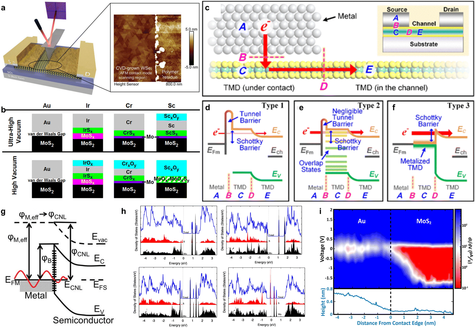
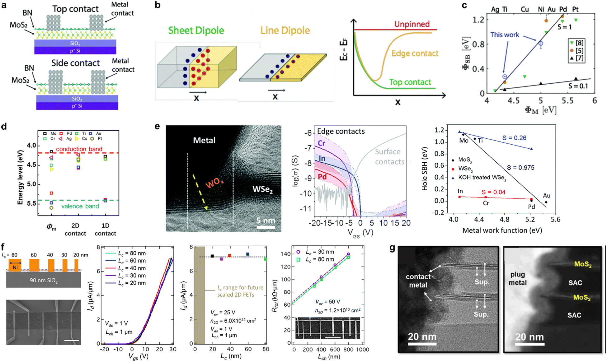
During the fabrication processes where metal–semiconductor junctions are established, the metal–semiconductor interface is susceptible to contamination. This contamination can be induced by adsorption of atmospheric gases91,92 or polymeric residues93,94 during fabrication processes (Fig. 2(a)). These contaminants not only prevent direct contact between metals and semiconductors but also lead to inadvertent changes in the electrical properties of semiconductors,93,95 thereby deviating the metal–semiconductor interfaces from their ideal configurations. Furthermore, reactive metals such as Ti, Cr, and Ir are prone to react with underlying 2D semiconductors and form an intermediate layer between metals and 2D semiconductors (Fig. 2(b)).96,97 This reaction could be beneficial for achieving lower resistance,98 similar to the successfully introduced silicidation process in Si technology.99,100 On the other hand, it can also degrade the contact interface and overall contact resistance. Thus, the reactivity of contact metals with 2D semiconductors should also be considered to form desirable metal–2D semiconductor contacts. In addition, there exists a physical separation between metals and 2D semiconductors due to the absence of dangling bonds on 2D semiconductors (Fig. 2(c)). This separation is called the van der Waals (vdW) gap and acts as an additional tunnelling barrier, further increasing the contact resistance.78,101 Utilization of inert metals such as gold (Au) can lead to the formation of type 1 junctions, whereas utilization of more reactive metals can lead to the formation of type 2 and type 3 junctions (Fig. 2(e) and (f)). Type 2 junctions represent metal/2D semiconductor junctions with medium bonding, where vdW gaps are negligible (Fig. 2(e)). Type 3 junctions indicate metal/2D semiconductor junctions with strong bonding, where 2D semiconductors under contact are metallized and vdW gaps vanish (Fig. 2(f)).
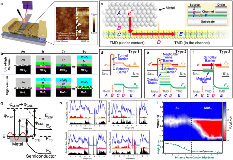 |
| | Fig. 2 (a) The surface of WSe2 before and after cleaning the post-lithography polymer residue. Reprinted from ref. 93 with permission from John Wiley and Sons. (b) Reactivity of gold (Au), iridium (Ir), chromium (Cr), and scandium (Sc) with MoS2. While Au forms van der Waals (vdW)-type contacts with MoS2, Ir, Cr, and Sc react with MoS2. Reproduced from ref. 96. (c)–(f) Schematic of metal/2D semiconductor junctions. (d) Type 1 indicates junctions with large vdW gaps and weak interaction, (e) type 2 indicates junctions with medium interaction and (f) type 3 indicates junctions with strong interaction. Reprinted from ref. 101. (g) Fermi-level pinning (FLP) phenomenon due to interface states. Reprinted from ref. 102 with permission from AIP Publishing. (h) Defect-induced gap-states (DIGS) from sulphur (S) vacancies and molybdenum (Mo) vacancies in MoS2. Reprinted from ref. 103 with permission from IOP Publishing. (i) dI/dV profiles of Au–MoS2 junctions, indicating gap states decaying with respect to the distance from the contact edge. Reprinted with permission from ref. 104. Copyright 2017 American Chemical Society. | |
2-2. Fermi-level pinning phenomenon due to MIGS and DIGS
When metals and semiconductors are in contact and in equilibrium, their Fermi level aligns through the transfer of charged carriers from one side to another. However, when there are numerous amounts of interface states within the forbidden gap of semiconductors (gap states) (Fig. 2(g)),102 a slight change in Fermi-level at the semiconductor surface can generate enough carriers that compensate for the Fermi-level difference. Therefore, the position of the Fermi-level at metal–semiconductor junctions rarely changes, regardless of a metal's Fermi-level. This phenomenon is called Fermi-level pinning (FLP) and it prevails in most metal–semiconductor junctions. The gap states exhibit either donor-like or acceptor-like states based on their charging behavior. When filled with electrons, acceptor-like states are negatively charged, whereas when empty, donor-like states are positively charged. Thus, charge neutrality necessitates the Fermi level of metals at metal/semiconductor junctions to align approximately with the branching point between acceptor-like and donor-like states. This branching point is referred to as the charge neutrality level (CNL), around which the Fermi level of metals at metal/semiconductor junctions is pinned.105–107 Typically, these gap states are classified as defect-induced gap states (DIGS) and metal-induced gap states (MIGS), according to their origins. Despite the dangling-bond-free nature of 2D semiconductors, native defects such as transition metal vacancies or chalcogen vacancies exist.108 Furthermore, defects can be generated during fabrication processes such as metal deposition.14 These defects can induce electronic states within the band gap (DIGS) (Fig. 2(h)).103 Similarly, metal contacts can also induce gap states. The wavefunctions of metal electrons can penetrate the semiconductor, decaying exponentially with respect to the distance from the interface (Fig. 2(i)).104,109 These exponentially decaying wavefunctions can have electronic states within the bandgap of semiconductors that correspond to the virtual gap states of the complex band structure of the semiconductors.110 Briefly, metal electrons’ wavefunctions penetrate the semiconductors, inducing exponentially decaying gap states (MIGS).104,109,110 DIGS and MIGS are responsible for the FLP phenomenon, forming a non-ideal Schottky barrier height (SBH) and leading to higher contact resistance.
3. Efforts to reduce contact resistance at metal/2D semiconductor junctions
3-1. Contact interface engineering
As aforementioned, the interface contaminants, the vdW gaps, and the FLP phenomenon play a major role in determining contact resistance. Among these, the FLP phenomenon (non-ideal SBH formation) is the main contributor to the high contact resistance issue occurring in metal/2D semiconductor junctions. Unlike Si technology, where the contact resistance can be greatly reduced through doping,111 no established doping techniques exist for 2D semiconductors. Therefore, alleviating the FLP phenomenon has been recognized to be crucial for overcoming the high contact resistance issue in 2D semiconductors. Utilization of interlayers at the contact interfaces can separate metals and 2D semiconductors, thereby suppressing the MIGS. Furthermore, it can protect 2D semiconductors during the fabrication process and provide clean contact interfaces, reducing the DIGS.
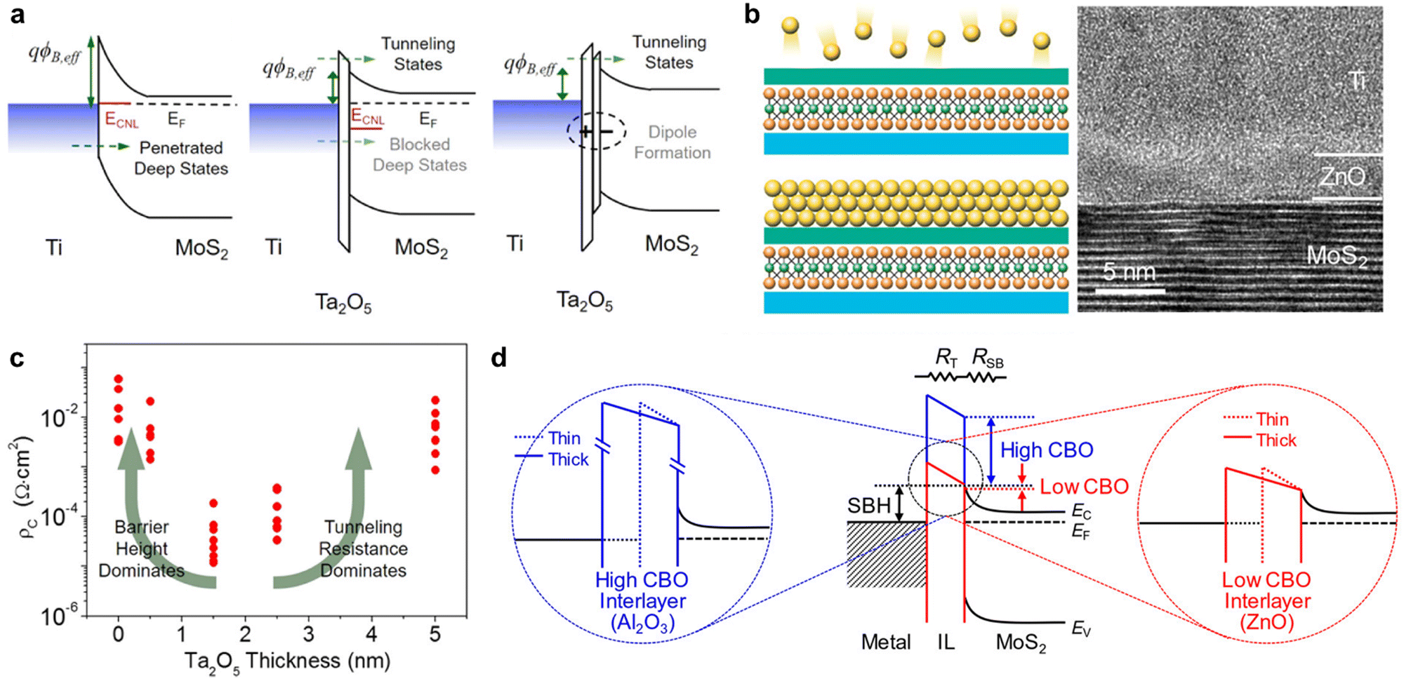
3-1-1. Metal–insulator–semiconductor contacts. Insulators can serve as effective contact interlayers, physically separating metals and 2D semiconductors. Because insulators have a larger bandgap and lower density of states than semiconductors, they suppress MIGS when used as contact interlayers (Fig. 3(a)).15
 |
| | Fig. 3 (a) Schematic of metal–insulator–semiconductor (MIS) contacts. MIGS are suppressed by inserting insulators and the interaction between metals and insulators can change the relative workfunctions of metals to semiconductors. Reprinted with permission from ref. 15. Copyright 2016 American Chemical Society. (b) Surface of 2D semiconductors protected by insulators during the metallization process and a transmission electron microscopy (TEM) image of the Ti/ZnO/MoS2 interface. Reprinted with permission from ref. 16. Copyright 2020 American Chemical Society. (c) Specific contact resistivity of Ti/Ta2O5/MoS2 junctions versus thickness of Ta2O5. Reprinted with permission from ref. 15. Copyright 2016 American Chemical Society. (d) Band diagram of MIS contacts with different conduction band offsets (CBO). ZnO shows a lower CBO than Al2O3, leading to lower tunneling resistance. Reprinted with permission from ref. 16. Copyright 2020 American Chemical Society. | |
Furthermore, insulators can protect underlying 2D semiconductors during the metal deposition process (Fig. 3(b)),16 reducing the generation of defects and DIGS. Consequently, the FLP phenomenon can be mitigated through the insertion of thin insulating layers. This contact strategy is called metal–insulator–semiconductor (MIS) contacts.15–18 One of the notable features of MIS contacts is that the interaction between metals and insulators forms interfacial dipoles and alters the relative work functions of metals to semiconductors.17,18 Cui et al. have reported that the work function of cobalt (Co) film on monolayer h-BN is 3.3 eV, which is 1.7 eV smaller than that of isolated Co.17 Similarly, Wang et al. have reported that the SBH decreases from 159 to 31 meV when few layer h-BN is inserted between Ni and MoS2, even though the Schottky–Mott rule14,112–114 would expect higher SBH for Ni–MoS2 junctions.18,89 Certainly, the thickness of insulators is one of the key factors in designing MIS contacts. As the thickness of insulators increases, the FLP phenomenon weakens more due to the greater suppression of MIGS, leading to a lower SBH. However, overall contact resistance may increase with thicker insulators due to increased tunnelling resistance across the insulators. Therefore, MIS contacts have the optimal insulator thickness for minimizing overall contact resistance (Fig. 3(c))15,16 and lowering tunnelling resistance is crucial for achieving low contact resistance in MIS contacts. Since tunnelling probability is also related to the height of the tunnelling barrier, a band offset between insulators and semiconductors should be considered when designing MIS contacts. Jang et al. have demonstrated that MIS contact with ZnO displays a lower contact resistance than that of Al2O3 due to a lower conduction band offset (Fig. 3(d)).16 Although MIS contacts exhibit small SBH on the order of a few tens of meV, reported instances demonstrate relatively high contact resistance on the order of several kΩ μm. (Table 1). Furthermore, in the advanced technological nodes, integrating insulators thick enough to prevent the FLP phenomenon can be challenging due to the limited space available for forming metal contacts. Thus, low contact resistance with ultrathin insulators should be achieved for the practical utilization of MIS contacts in advanced technological nodes.
Table 1 Comparison table for MIS contacts, vdW contacts, vdW-type contacts, edge contacts, and semimetal contacts
| Method |
Channel material |
Contact material |
Type |
Contact resistance [kΩ μm] |
Schottky barrier height [meV] |
On-current [μA μm−1] |
L [μm] |
Ref. |
| IRDS Si HP target (2037) |
Si |
— |
— |
<0.105 |
— |
753 |
0.012 |
83 |
| IRDS Si HD target (2037) |
547 |
| MIS contact |
Exfoliated 1L MoS2 |
h-BN/Co |
n |
3.8 |
16 |
∼1 (VDS = 0.01 V) |
0.2 |
17 |
| Exfoliated 4–5L MoS2 |
h-BN/Ni |
n |
1.8 |
31 |
330 (VDS = 5 V) |
0.3 |
18 |
| Exfoliated 8 nm MoS2 |
ZnO/Ti |
n |
0.9 |
32 |
<1.5 (VDS = 0.5 V) |
2 |
16 |
| CVD 4L MoS2 |
Ta2O5/Ti |
n |
— |
29 |
— |
1 |
15 |
| VdW contact |
Exfoliated 7 nm WSe2 |
NbWSe2/Ti |
p |
0.3 |
— |
320 (VDS = −1.5 V) |
0.27 |
19 |
| Exfoliated 12 nm WSe2 |
NbMoS2 |
p |
<5 |
— |
4.8 (VDS = −0.1 V) |
16 |
22 |
| Exfoliated 8–12 nm WSe2 |
Cl–SnSe2 |
p |
114 |
780 |
>4 (VDS = 1 V) |
— |
23 |
| CVD 1L MoS2 |
NbS2/Cr |
n |
<7500 |
— |
— |
10 |
20 |
| CVD 1L WSe2 |
1T′-WS2/Au |
p |
3.07 |
50 |
<1.1 (VDS = 1 V) |
15 |
25 |
| CVD 1L MoS2 |
WTe2/Ti |
n |
67 |
100 |
0.244 (VDS = 1 V) |
15 |
27 |
| CVD 1L WSe2 |
WTe2/Ti |
p |
— |
71 |
— |
— |
21 |
| CVD 2L WSe2 |
VSe2/Cr |
p |
<0.25 |
— |
1580 (VDS = 1 V) |
0.02 |
24 |
| CVD 5–6 L MoTe2 |
1T′-MoTe2/Au |
p |
0.7 |
14 |
7.8 (VDS = −1 V) |
2 |
26 |
| Exfoliated 2L MoS2 |
ZrTe2/Au |
n |
— |
−13.4 |
259 (VDS = 2 V) |
0.25 |
28 |
| Exfoliated 5–6 nm MoS2 |
Graphene/Ti/Au |
n |
3.7 |
— |
161 (VDS = 4 V) |
1 |
29 |
| Exfoliated 16 nm MoS2 |
Graphene/Ni |
n |
0.26 |
300 |
>4.5 (VDS = 0.2 V) |
1 |
30 |
| Exfoliated 5L MoS2 |
Graphene/Cr/Au |
n |
7.5 |
— |
— |
0.035 |
31 |
| Exfoliated 1L MoS2 |
Graphene |
n |
4.8 |
— |
8.1 (VDS = 0.1 V) |
0.008 |
32 |
| CVD 1L MoS2 |
Graphene |
n |
115 |
0.19 |
— |
4 |
33 |
| VdW-type contact |
Exfoliated 2L WSe2 |
Pd/Au |
p |
3.5 |
— |
>5 (VDS = 0.1 V) |
1 |
34 |
| Exfoliated <10 nm WSe2 |
In |
n |
— |
−23 |
<1 (VDS = 0.1 V) |
2.5 |
36 |
| Exfoliated <10 nm WSe2 |
Ti |
n |
— |
64 |
<0.01 (VDS = 0.1 V) |
7.4 |
| Exfoliated <10 nm WSe2 |
Au |
p |
— |
120 |
<1 (VDS = 0.1 V) |
2.9 |
| Exfoliated <10 nm WSe2 |
Pd |
p |
— |
−15 |
>1 (VDS = 0.1 V) |
2.9 |
| Exfoliated <10 nm WSe2 |
Pt |
p |
— |
−45 |
0.1 (VDS = 0.1 V) |
2.6 |
| CVD 1L WSe2 |
Au |
p |
9 |
47 |
>3 (VDS = 1 V) |
7.8 |
37 |
| Exfoliated 1L WSe2 |
Pt/Au |
p |
5 |
— |
7.4 (VDS = −1 V) |
3 |
39 |
| CVD 1L WSe2 |
Au |
— |
10.2 |
— |
— |
— |
41 |
| CVD 1L WSe2 |
Pd |
— |
5.3 |
36 |
— |
— |
| CVD 1L WSe2 |
Ag |
— |
2.75 × 10⁴ |
116 |
— |
— |
| CVD 1L WSe2 |
Ti |
— |
3900 |
103 |
— |
— |
| CVD 1L MoS2 |
In/Au |
n |
3.3 |
— |
18 (VDS = 1 V) |
2 |
35 |
| CVD 1L WSe2 |
Pt |
p |
229 |
400 |
7.6 (VDS = 1 V) |
1.5 |
40 |
| Exfoliated 4–20 nm MoS2 |
Ag |
n |
— |
20 |
660 |
0.16 |
14 |
| VdW-type contact |
Exfoliated 4–20 nm MoS2 |
Pt |
p |
— |
67 |
210 |
0.14 |
14 |
| Exfoliated 12 nm WSe2 |
Au |
p |
1.25 |
60 |
— |
1.6 |
38 |
| Edge contact |
CVD 2L MoS2 |
Ni |
n |
31 |
— |
— |
— |
42 |
| Exfoliated 1L MoS2 |
Ti |
n |
8.3 |
— |
50 (VDS = 3 V) |
1 |
43 |
| Exfoliated 4.6 nm MoS2 |
Mn |
n |
∼700 |
— |
— |
— |
46 |
| Exfoliated 7.5 nm MoS2 |
Pd |
p |
— |
10 |
3.9 (VDS = 1 V) |
9 |
44 |
| Exfoliated 82 nm MoS2 |
Au |
p |
— |
−16 |
3.5 (VDS = 1 V) |
10 |
| Exfoliated <10 nm WSe2 |
In |
p |
— |
74 |
— |
— |
45 |
| Exfoliated <10 nm WSe2 |
Cr |
p |
— |
70 |
— |
— |
| Exfoliated <10 nm WSe2 |
Pd |
p |
— |
36 |
— |
— |
| CVD 1L MoS2 |
Ni |
n |
— |
850 |
— |
— |
47 |
| CVD 1L MoS2 |
Ti |
n |
— |
210 |
— |
— |
| Semimetal contacts |
CVD 1L MoS2 |
Bi |
n |
0.123 |
0 |
1135 (VDS = 1.5 V) |
0.035 |
12 |
| CVD 1L MoS2 |
Sb |
n |
0.042 |
−10 |
1440 (VDS = 1 V) |
0.02 |
13 |
| CVD 1L MoS2 |
Sb/Au |
n |
0.300 |
— |
>200 (VDS = 1 V) |
0.1 |
66 |
| CVD 1L MoS2 |
Sb/Au |
n |
0.66 |
— |
600 (VDS = 1 V) |
0.05 |
67 |
| CVD 1L MoS2 |
Sn/Au |
n |
0.84 |
30 |
480 (VDS = 1 V) |
0.035 |
68 |
| CVD 1L MoS2 |
Bi/Au |
n |
0.28 |
0 |
461 (VDS = 1 V) |
0.06 |
69 |
| CVD 1L WS2 |
Bi/Ti/Au |
n |
1.3 |
40 |
245 (VDS = 4.1 V) |
0.32 |
70 |
| CVD 1L MoS2 |
Bi |
n |
0.111 |
0 |
1316 (VDS = 2.5 V) |
0.2 |
71 |
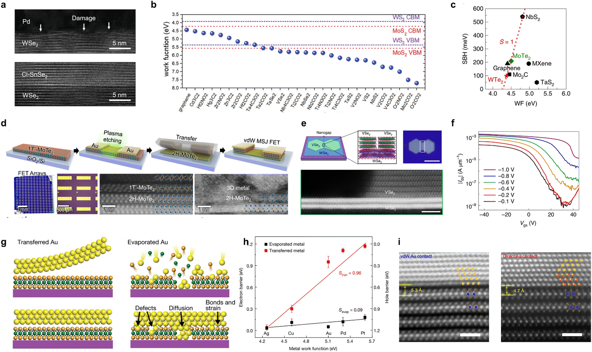
3-1-2. Van der Waals contacts. Metallic 2D materials can serve as contact interlayers as well, offering advantages over insulators in achieving lower contact resistance due to their intrinsic conductivity.115 Additionally, they interact with 2D semiconductors through the weak vdW forces, providing atomically sharp contact profiles separated by the vdW gaps (Fig. 4(a)). Therefore, the contact strategy utilizing metallic 2D materials refers to vdW contacts and eliminates the FLP phenomenon.19–27,116,117 VdW contacts between diverse 2D semiconductors and various metallic 2D materials, including heavily doped 2D semiconductors,19,22,23 inherently (semi)metallic 1T(′)-phase TMDs,20,21,24–28,116,117 and graphene29–33 have been investigated. The reported instances have demonstrated a wide range of contact resistance (Table 1), a consequence of the broad range of work functions offered by 2D materials (Fig. 4(b))118–120 and the absence of the FLP phenomenon in vdW contacts (Fig. 4(c)).27 Hence, it is crucial to carefully choose appropriate metallic 2D materials tailored to a specific 2D semiconductor to ensure low SBH and contact resistance. Utilizing graphene contacts is also advantageous in this regard. This is because the SBH between 2D semiconductors and graphene is modulated by electrostatic doping29,31 or charge transfer from metals.30,33 The Fermi-level of graphene is shifted largely by doping due to the negligible DOS around its Dirac point. VdW contacts can be achieved by transferring 2D materials onto each other (Fig. 4(d)).19,20,22,23,25,27,29–33,116 While this fabrication method is useful for quickly testing various vdW contacts and can circumvent thermal budgets through recent advancements in the transfer process of various 2D materials,121,122 it may induce larger vdW gaps, degrading overall contact resistance. Shim et al. have reported WTe2-contacted WSe2-channel transistors and compared them with palladium (Pd)-contacted WSe2-channel transistors.116 Devices with WTe2 contacts exhibit significantly lower electron and hole currents than Pd-contacted devices. This presents a substantial series resistance in WTe2-contacted devices, rather than the existence of a higher SBH at WTe2–WSe2 junctions compared to Pd–WSe2 junctions. Furthermore, transferring 2D materials would not be applicable for advanced transistor structures such as GAAs. In contrast to the transfer, direct growth of metallic 2D materials is desirable, providing clean contact interfaces with minimal vdW gaps (Fig. 3(e)).21,24,117 Notably, Wu et al. have demonstrated that metallic VSe2 can be grown directly on bilayer-WSe2, achieving a low contact resistance less than 0.25 kΩ μm and a high on-current exceeding 1.5 mA μm−1 (Fig. 4(e) and (f)).24 This on-current is among the highest values achieved thus far, even comparable to that of the Si transistors.83 However, growth of metallic 2D materials on 2D semiconductors at precise positions in the wafer-scale would be challenging, considering the current immature state of the wafer-scale growth technology for 2D materials.123 Nevertheless, their result suggests that vdW contacts, with the appropriate process technology suitable for mass production, have potential in enabling low contact resistance for 2D semiconductors.
 |
| | Fig. 4 (a) Cross-sectional TEM images of Pd–WSe2 junctions and Cl–SnSe2/WSe2 junctions. Cl–SnSe2/WSe2 junctions show intact interfaces while Pd–WSe2 junctions show damaged interfaces during the metallization process. Reprinted from ref. 23 with permission from John Wiley and Sons. (b) Workfunctions of various metallic TMDs with respect to the conduction band minimum (CBM) and valence band maximum (VBM) of MoS2 and WS2. Reprinted from ref. 120 with permission from John Wiley and Sons. (c) Schottky barrier height (SBH) between MoS2 and various metallic 2D materials, indicating suppressed Fermi-level pinning (FLP) phenomenon in vdW contacts. Reprinted from ref. 27 with permission from Springer Nature. (d) 1T′-MoTe2/2H-MoTe2 vdW contacts enabled by transferring 1T′-MoTe2 onto 2H-MoTe2 with atomically clean interfaces. Reprinted from ref. 26 (e) VSe2–WSe2 vdW contacts and (f) transfer curve of VSe2 contacted WSe2 channel FETs, displaying a high on-current exceeding 1.5 mA μm−1. Reprinted from ref. 24 with permission from Springer Nature. (g) Schematic illustration of vdW-type contacts enabled by the transfer process and metal/2D semiconductor junctions formed by the conventional evaporation process. Reprinted from ref. 14 with permission from Springer Nature. (h) Electron barrier versus metal workfunctions of vdW-type contacts and evaporated contacts. VdW-type contacts show suppressed FLP phenomenon. Reprinted from ref. 14 with permission from Springer Nature. (i) Scanning transmission electron microscopy (STEM) image of vdW-type Au–WSe2 junctions and directly deposited Au–Wse2 junctions. VdW-type Au–WSe2 junctions display enlarged vdW gaps. Reprinted from ref. 38 with permission from Springer Nature. | |
3-1-3. Van der Waals-type contacts. Conventional metals also establish junctions with 2D semiconductors, separated by the vdW gaps. These junctions can be achieved through a non-destructive formation of metals with minimal interaction with 2D semiconductors (Fig. 4(g)). This type of contacts is referred to as vdW-type contacts, and it can successfully eliminate the FLP phenomenon (Fig. 4(h)).14,34–41,124 VdW-type contacts can be achieved through various methods including transfer14,34,36,37,39,124 and utilization of decomposable buffer layers.38,41 However, these methods would not be suitable for advanced transistor structures such as GAA, where contacts need to be formed in limited and intricate 3D spaces, as discussed earlier. Therefore, vdW-type contacts with a direct metal deposition method would be more desirable. As vdW-type contacts can be established by minimizing the defect generation during the metallization process, selecting metals with low sublimation energy35 or optimizing the metallization process40 can lead to the formation of vdW-type contacts without relying on a transfer process or additional layers. Wang et al. reported that metals with low sublimation energy, such as indium (In), can form vdW-type contacts with 2D semiconductors through direct deposition.35 Notably, they also discovered that even high workfunction metals, such as platinum (Pt), can be gently deposited on 2D semiconductors without causing damage to them, when the sample temperature is maintained at room temperature.40 Their discovery indicates that any metal/2D semiconductor junctions could follow the Schottky-Mott rule if process conditions are optimized. The reported vdW-type contacts showed a relatively high contact resistance ranging from several kΩ μm to tens of kΩ μm (Table 1). This may be attributed to enlarged vdW gaps in vdW-type contacts, as Kwon et al. reported that vdW-type gold (Au)–WSe2 junctions exhibit larger vdW gaps than directly deposited Au–WSe2 junctions (Fig. 4(i)).38 These findings from vdW-type contacts highlight that achieving clean contact interfaces with minimal vdW gaps is crucial to accomplish ultra-low contact resistance for 2D semiconductors.
3-2. Edge contacts
Due to the large area-to-volume ratio of 2D semiconductors, metal/2D semiconductor junctions are typically formed on the surface of 2D semiconductors. However, surface contacts can often result in severe FLP phenomenon or the presence of large vdW gaps, leading to high contact resistance, as discussed earlier. Since 2D semiconductors consist of covalent bonds in the in-plane directions, there are unterminated bonds at their edges, similar to conventional semiconductors. When metals contact the edges, covalent bonds form between the metals and 2D semiconductors, eliminating vdW gaps (Fig. 5(a)).101 This contact strategy is called edge contacts and facilitates carrier injections from metals to semiconductors and vice versa, through strong interaction between metals and 2D semiconductors.42–45,101 Furthermore, theoretical studies have revealed that reduced contact dimensionality leads to alleviated FLP phenomenon. When gap states, which are responsible for FLP phenomenon, are charged by carriers, they can induce image charges on metal sides and form an interface dipole. In edge contacts, these dipoles are spatially localized in 1D contact interfaces and form a line of dipoles, inducing an electric field much weaker than that of a sheet of dipoles46,47,125–127 (Fig. 5(b)). Thus, the FLP phenomenon can be effectively alleviated in edge contacts. Alleviated FLP phenomenon was confirmed in various experimental studies.42,43,46,47 Yang et al. have demonstrated the suppressed FLP phenomenon in edge contacted metal/multilayer-MoS2 junctions (Fig. 5(c)).44 Hung et al. have reported that edge contacts can effectively suppress FLP phenomenon even for monolayer MoS2.21 Consequently, the quality of the contact interface remains crucial to suppress the FLP phenomenon in edge contacts. During the fabrication process, the edges of 2D semiconductors can be exposed to contaminants, which leads to stronger FLP phenomenon. Ngo et al. reported that non-stoichiometric WOx can form at the edges of WSe2 and it induces stronger FLP as WOx has a high workfunction (Fig. 5(d)).45 Notably, edge contacts are immune to contact length scaling, as their contact area does not change with contact length. Cheng et al. demonstrated that the on-current of edge-contacted MoS2 devices does not decrease even though the contact length shrinks to 20 nm (Fig. 5(e)).42 However, edge contacts typically show higher contact resistance than surface contacts (Table 1), as edge contacts cannot provide sufficient contact area.46 Surface contacts alone would not provide sufficiently low contact resistance, either, due to the limited contact space in advanced technological nodes. Therefore, wrap-around contacts that integrate edge and surface contacts might be more desirable to maximize the contact area and ensure low contact resistance, as Chung et al. have recently demonstrated in MoS2-channel devices.128
 |
| | Fig. 5 (a) Schematic diagram of edge contacts and high-resolution transmission electron microscopy (HR-TEM) image of edge contacted MoS2. Reprinted from ref. 44 with permission from John Wiley and Sons. (b) Relative energy level of the conduction band minimum with respect to the Fermi level of ideal, top contacted, and edge contacted junctions. Reprinted from ref. 47 with permission from IEEE. (c) The workfunction of metals and band alignment of top contacted and edge contacted metal/2D semiconductor junctions, indicating reduced FLP phenomenon in edge contacts. Reprinted from ref. 44 with permission from John Wiley and Sons. (d) Cross sectional HRTEM image of edge contacted metal–WSe2 junctions, displaying the presence of WOx at the interface, transfer characteristics of edge contacted WSe2-channel devices and surface contacted WSe2-channel devices, indicating persistent p-type characteristics in edge contacted devices, and hole SBH versus metal workfunctions. Reprinted from ref. 45 with permission from Royal Society of Chemistry. (e) Contact length scaling for nickel (Ni) edge contacted MoS2-channel devices, showing immunity to contact length scaling down to 20 nm. Reprinted with permission from ref. 42. Copyright 2019 American Chemical Society. | |
3-3. Doping
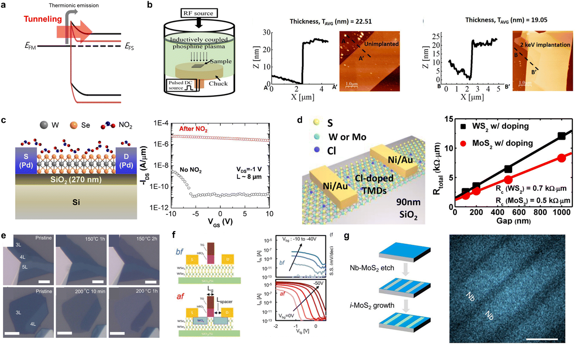
Heavily doped semiconductors can readily form Ohmic junctions with various metals, as carriers can easily tunnel thin barriers (Fig. 6(a)). In Si technology, this can be achieved by substituting Si atoms with group III or group V elements.129 However, an ion implantation, which is mostly used to dope the Si, is not readily applicable for atomically thin 2D semiconductors due to substantial defect generation during an ion bombardment process (Fig. 6(b)),130 prompting the exploration of alternative doping approaches. Since the early stage of doping research for 2D semiconductors, chemical doping has been explored due to their facileness (Table 2).48–56 Although utilization of chemicals has proven useful in inducing heavy doping on 2D semiconductors and achieving low contact resistance (Fig. 6(c) and (d)), they often suffer from poor stability and controllability, making them unsuitable for practical applications. More stable doping of 2D semiconductors can be achieved using solid-state oxide layers. Solid-state oxides can induce substantial charges on 2D semiconductors, providing more stable heavily doped 2D semiconductors (Table 2).57–64,131,132 Notably, WOx can be formed by oxidizing tungsten (W)-based TMDs, inducing substantial hole doping on the remaining W-based TMDs. Furthermore, WOx can be formed through a self-limiting oxidation process, making a sophisticated layer-by-layer oxidation of W-based TMDs possible (Fig. 6(e)).58,60,62,132 Huang et al. have demonstrated that this layer-by-layer oxidation of bilayer WSe2 can be utilized to establish a WOx spacer, inducing heavy hole doping on the spacer region of WSe2-channel FETs (Fig. 6(f)).62 However, doping the contact area through solid-state oxides is challenging, as inserting them between metals and 2D semiconductors leads to undesirable resistance.59 In contrast to this, substitutional doping can induce substantial charges on 2D semiconductors without an additional layer. In situ substitutional doping, where dopant atoms are incorporated into lattice structures during their growth, is available for 2D semiconductors. This technique provides the most stable heavily doped 2D semiconductors, compared to the other approaches (Table 2).65,133–136 However, with this in situ substitutional doping technique, selectively doping a specific area of 2D semiconductors is challenging. Therefore, a regrowth strategy, where heavily doped 2D semiconductors for contacts and intrinsic 2D semiconductors for channels are grown separately, could be useful to circumvent this challenge, as Gao et al. have demonstrated (Fig. 6(g)).135
Table 2 Comparison table for doping
| Method |
Channel material |
Contact material |
Type |
Contact resistance [kΩ μm] |
Carrier concentration [1012 cm−2] |
On-current [μA μm−1] |
L [μm] |
Ref. |
| IRDS Si HP target (2037) |
Si |
— |
— |
<0.105 |
— |
753 |
0.012 |
83 |
| IRDS Si HD target (2037) |
547 |
| NO2 doping |
Exfoliated 1L WSe2 |
Pd |
p |
— |
2.2 |
<10 (VDS = −1 V) |
9.4 |
48 |
| BV doping |
Exfoliated 5 nm MoS2 |
Ni/Au |
n |
1.1 |
12 |
8 (VDS = 0.05 V) |
0.42 |
49 |
| Cl doping |
Exfoliated 5–7L WS2 |
Ni |
n |
0.7 |
0.6 |
380 (VDS = 2 V) |
0.1 |
50 |
| Cl doping |
Exfoliated 5–7L MoS2 |
Ni |
n |
0.5 |
9.2 |
460 (VDS = 2 V) |
0.1 |
|
| NO2 doping |
Exfoliated 7 nm WSe2 |
Pd |
p |
1.27 |
11.2 |
— |
0.5 |
51 |
| LiF doping |
Exfoliated 5.3 nm WS2 |
Cr/Au |
n |
0.93 |
— |
65 (VDS = 1 V) |
0.5 |
52 |
| AuCl doping |
Exfoliated 7–11 nm MoS2 |
Pd/Au |
p |
2.3 |
1.5 |
21 |
1 |
53 |
| Nbm doping |
Exfoliated 1L MoS2 |
Au |
n |
4.4 |
2.18 |
83.4 (VDS = 1 V) |
0.5 |
54 |
| Carbonyl compound doping |
CVD 1L MoS2 |
Au |
n |
1.2 |
41 |
— |
— |
55 |
| HAuCl4 doping |
CVD 1L WSe2 |
Pd |
p |
0.7 |
17.6 |
~10 (VDS = −1 V) |
5 |
56 |
| ATO doping |
Exfoliated 1L MoS2 |
Ag/Au |
n |
0.18 |
7.4 |
240 (VDS = 2 V) |
0.45 |
57 |
| AlOx doping |
CVD 1L MoS2 |
Au |
n |
0.48 |
20 |
300 (VDS = 1 V) |
0.38 |
61 |
| SiOx doping |
CVD 1L MoS2 |
Pd |
n |
4.5 |
14 |
— |
5 |
63 |
| WOx doping |
CVD 1L WSe2 |
Pd/Au |
p |
1.45 |
0.6 |
1 (VDS = 0.1 V) |
0.5 |
64 |
| WOx doping |
Exfoliated 4L WSe2 |
Ti/Au |
p |
1.4 |
2.6 |
— |
— |
58 |
| WOx doping |
Exfoliated 8L WSe2 |
Ti/Pd |
p |
0.528 |
8.3 |
320 (VDS = −1 V) |
0.07 |
60 |
| WOx doping |
CVD 2L WSe2 |
Pd |
p |
1 |
— |
>10 |
0.5 |
62 |
| MoOx doping |
Exfoliated few L WSe2 |
Pt |
p |
0.8 |
20 |
1000 (VDS = 5 V) |
0.4 |
59 |
| Fe doping |
CVD 1L MoS2 |
Cr/Au |
n |
0.678 |
76 |
— |
10 |
65 |
 |
| | Fig. 6 (a) Band diagram of undoped (black) and doped (red) metal–semiconductor junctions. The tunnelling current increases in doped junctions through a thinned barrier due to doping. (b) A schematic of an ion implantation system and thickness reduction of MoS2 flakes measured by atomic force microscopy, due to an ion implantation process. Reprinted with permission from ref. 130. Copyright 2016 American Chemical Society. (c) A schematic diagram of NO2 doped WSe2 channel FETs and their transfer characteristics, indicating heavily doped WSe2. Reprinted with permission from ref. 48. Copyright 2012 American Chemical Society. (d) Schematic diagram of Cl doped TMDs and contact resistance of doped Ni–WS2 and Ni–MoS2 junctions. Reprinted with permission from ref. 50. Copyright 2014 American Chemical Society. (e) Self-limiting oxidation of WSe2 by O3 treatment. Reprinted with permission from ref. 132 (f) P-MOSFET enabled by self-limiting oxidation of bilayer WSe2. Only the top layer was oxidized and induce hole doping on underlying WSe2. Reprinted with permission from ref. 62. (g) Nb-doped MoS2 and pristine Mos2 junctions formed by regrowing intrinsic MoS2 after etching Nb-doped MoS2. Reprinted with permission from ref. 135. Copyright 2020 American Chemical Society. | |
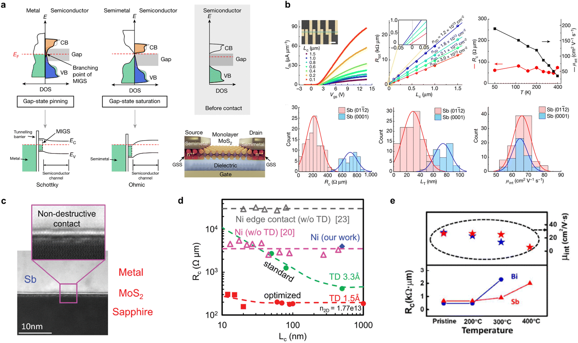
3-4. Semimetal contacts
MIGS, one of the main contributors of the FLP phenomenon, are induced by the penetration of electron wavefunctions from metals into semiconductors when metal/semiconductor junctions are formed.109,110 In contrast to metals, which possess a significant density of states (DOS) around their Fermi level, semimetals have a negligible DOS at their Fermi level, resulting in significantly reduced MIGS. According to the theory of MIGS, MIGS are contributed by either the conduction band or valence band. Conduction band-contributed MIGS are acceptor-like states and the valence band-contributed MIGS are donor-like states.107 When semimetals come into contact with semiconductors and the Fermi level of semimetals is close to the conduction band minimum of semiconductors, the contribution of the conduction band to MIGS is greatly reduced and MIGS are mainly contributed by the valence band. This shifts the branching point of MIGS, where the Fermi-level of metals is pinned around,107 into the conduction band (Fig. 7(a)).12 Therefore, the SBH of the junctions vanishes and semiconductors under contact become heavily doped by electrons, leading to ohmic contacts.12,13,66–70,137–140 Furthermore, as semimetals typically have a low melting point, vdW-type contacts are achievable with semimetals, leading to clean contact interfaces (Fig. 7(c)).66 Shen et al. have reported that semimetal bismuth (Bi) (0001) can form ohmic junctions with MoS2, reporting a negligible SBH, low contact resistance of 123 Ω μm, and high on-current of 1135 μA μm−1,12 even comparable that of the state-of-the-art Si transistors.83 They have also noted that the quality of channel material is crucial to achieve low contact resistance with semimetal contacts, since DIGS from high defect density can affect the Fermi level pinning. The crystal orientation of semimetals also affects the contact resistance. Li et al. demonstrated that semimetal antimony (Sb) (01![[1 with combining macron]](https://www.rsc.org/images/entities/char_0031_0304.gif) 2)–MoS2 junctions can outperform Sb (0001)–MoS2 junctions, as Sb (012) has a higher atomic density than Sb (0001), leading to stronger interaction between Sb (012) and MoS2 (Fig. 7(b)).13 This results in an ultra-low contact resistance of 42 Ω μm and high on current of 1.23 mA μm−1, which even outperforms that of the state-of-the-art Si technology.83 Notably, semimetal contacts also exhibit a short transfer length.12,13 Wu et al. demonstrated that the contact length of Sb–MoS2 junctions can be scaled down to 12 nm without degrading performance when process conditions are optimized to ensure a minimal vdW gap (Fig. 7(d)).66 Thus far, semimetal contacts have only been demonstrated for achieving n-type ohmic contacts, as elemental semimetals typically have a low workfunction. p-Type ohmic contacts can be achieved, if semimetals’ workfunction aligns with the valence band maximum of 2D semiconductors, as Yang et al. have theoretically demonstrated.141 They have also noted that high workfunction semimetals such as Co3Sn2S2 and TaP can form ohmic contacts for holes with WSe2. Even though semimetal contacts offer ultralow contact resistance, they encounter challenges regarding their poor thermal stability due to their low melting point, especially for Bi (271.5 °C). Although Sb shows better thermal stability due to its higher melting point (630.6 °C), the performance of Sb–MoS2 junctions starts degrading at 300 °C (Fig. 7(e)).67
2)–MoS2 junctions can outperform Sb (0001)–MoS2 junctions, as Sb (012) has a higher atomic density than Sb (0001), leading to stronger interaction between Sb (012) and MoS2 (Fig. 7(b)).13 This results in an ultra-low contact resistance of 42 Ω μm and high on current of 1.23 mA μm−1, which even outperforms that of the state-of-the-art Si technology.83 Notably, semimetal contacts also exhibit a short transfer length.12,13 Wu et al. demonstrated that the contact length of Sb–MoS2 junctions can be scaled down to 12 nm without degrading performance when process conditions are optimized to ensure a minimal vdW gap (Fig. 7(d)).66 Thus far, semimetal contacts have only been demonstrated for achieving n-type ohmic contacts, as elemental semimetals typically have a low workfunction. p-Type ohmic contacts can be achieved, if semimetals’ workfunction aligns with the valence band maximum of 2D semiconductors, as Yang et al. have theoretically demonstrated.141 They have also noted that high workfunction semimetals such as Co3Sn2S2 and TaP can form ohmic contacts for holes with WSe2. Even though semimetal contacts offer ultralow contact resistance, they encounter challenges regarding their poor thermal stability due to their low melting point, especially for Bi (271.5 °C). Although Sb shows better thermal stability due to its higher melting point (630.6 °C), the performance of Sb–MoS2 junctions starts degrading at 300 °C (Fig. 7(e)).67
 |
| | Fig. 7 (a) Schematic diagram of metal/semiconductor junctions and semimetal/semiconductor junctions. Junctions with semimetals show suppressed MIGS and almost zero SBH. Reprinted from ref. 12 with permission from Springer Nature. (b) Electrical properties of antimony (Sb) (012)–MoS2 junctions and Sb (0001)–MoS2 junctions, indicating the superior performance of Sb (012)–MoS2 junctions. Reprinted from ref. 13 with permission from Springer Nature. (c) vdW-type contacts between Sb and MoS2 due to the low melting point of Sb. Reprinted from ref. 66 with permission from IEEE. (d) Contact length scaling of Ni- and Sb–MoS2 junctions, indicating superior immunity to the contact length scaling of Sb–MoS2 junctions. Reprinted from ref. 66 with permission from IEEE. (e) Contact resistance of bismuth (Bi)– and Sb–MoS2 junctions versus annealing temperature. The performance of Sb–MoS2 junctions starts degrading at 300 °C. Reprinted from ref. 67 with permission from IEEE. | |
4. Perspectives and conclusions
We have discussed the potential of 2D semiconductors as an alternative channel material for advanced 3D-structured transistors, such as GAAFETs and CFETs. This potential arises from their decent carrier mobility even at sub 1 nm thickness and much shorter scaling length than that of silicon. However, 2D semiconductors suffer from high contact resistance due to the FLP phenomenon and vdW gaps, significantly degrading their on-current and circuit level performance. Moreover, addressing this becomes even more formidable in advanced technological nodes, where contacts must be established in intricate and limited 3D spaces. This limitation can restrict options for contact engineering strategies. In this regard, we have reviewed and evaluated the contact engineering technologies for 2D semiconductors such as MIS contacts, vdW and vdW-type contacts, doping-assisted, and semimetal contacts.
Most contact innovations have thus far been accomplished in planar-structured devices with large dimensions. This significantly deviates from advanced 3D transistor structures such as GAAFETs, where contacts need to be formed under limited and complex 3D spaces. This discrepancy could raise questions about their suitability for practical applications. Due to complex 3D space allowed for contacts, the insertion of contact interlayers except metals would not be desirable. Similarly, vdW and vdW-type contacts utilizing a transfer process would also be inapplicable. Furthermore, the shrunken device size in advanced technological nodes leaves not much area reserved for contacts. As most of the contact engineering techniques were reported with very large dimensions, significantly higher contact resistances are predicted when applied to the scaled devices. Therefore, rather than relying solely on surface contact not to provide sufficient contact area, edge or wrap-around contacts based on ALD of various metals need to be explored.
Thus far, significant advancements have been made in lowering contact resistance. In particular, ultra-low contact resistance for electrons has been achieved through the introduction of semimetal contacts, although their thermal stability issues remain. However, the contact resistance for holes remains relatively high, which needs to be improved for practical applications of 2D semiconductors. The findings from various technical innovations concluded that suppression of the FLP phenomenon alone would be insufficient to achieve ultra-low contact resistance. Thus, alternative approaches such as substitutional doping should be considered to achieve ultra-low contact resistance for holes. Finally, it should be emphasized that considering the 3D device structures is very important to achieve reliable results and facilitate the practical integration of 2D semiconductors.
Conflicts of interest
There are no conflicts to declare.
Acknowledgements
This research was supported by the National Research Foundation of Korea (NRF) (2022M3F3A2A01072215, 2021R1A2C2010026). This work was also supported by the Technology Innovation Program (RS-2023-00235609, Proposal of 3D DRAM development direction from the process development of vertical stacked cell transistors) funded by the Ministry of Trade, Industry & Energy (MOTIE, Korea) (1415187471). It was also supported by Samsung Electronics Co., Ltd (IO231207-08190-01).
Notes and references
- R. H. Dennard, F. H. Gaensslen, H.-N. Yu, V. L. Rideout, E. Bassous and A. R. LeBlanc, IEEE, J. Solid State Circ., 1974, 9, 256–268 Search PubMed.
- M. M. Frank, presented in part at the 2011 Proceedings of the European Solid-State Device Research Conference (ESSDERC), 2011.
- A. Razavieh, P. Zeitzoff and E. J. Nowak, IEEE Trans. Nanotechnol., 2019, 18, 999–1004 CAS.
- N. Loubet, T. Hook, P. Montanini, C. W. Yeung, S. Kanakasabapathy, M. Guillom, T. Yamashita, J. Zhang, X. Miao, J. Wang, A. Young, R. Chao, M. Kang, Z. Liu, S. Fan, B. Hamieh, S. Sieg, Y. Mignot, W. Xu, S. C. Seo, J. Yoo, S. Mochizuki, M. Sankarapandian, O. Kwon, A. Carr, A. Greene, Y. Park, J. Frougier, R. Galatage, R. Bao, J. Shearer, R. Conti, H. Song, D. Lee, D. Kong, Y. Xu, A. Arceo, Z. Bi, P. Xu, R. Muthinti, J. Li, R. Wong, D. Brown, P. Oldiges, R. Robison, J. Arnold, N. Felix, S. Skordas, J. Gaudiello, T. Standaert, H. Jagannathan, D. Corliss, M. H. Na, A. Knorr, T. Wu, D. Gupta, S. Lian, R. Divakaruni, T. Gow, C. Labelle, S. Lee, V. Paruchuri, H. Bu and M. Khare, presented in part at the 2017 Symposium on VLSI Technology, 2017.
- S. Barraud, B. Previtali, C. Vizioz, J. M. Hartmann, J. Sturm, J. Lassarre, C. Perrot, P. Rodriguez, V. Loup, A. Magalhaes-Lucas, R. Kies, G. Romano, M. Cassé, N. Bernier, A. Jannaud, A. Grenier and F. Andrieu, 2020.
- A. Veloso, G. Eneman, A. de Keersgieter, D. Jang, H. Mertens, P. Matagne, E. D. Litta, J. Ryckaert and N. Horiguchi, presented in part at the 2021 5th IEEE Electron Devices Technology & Manufacturing Conference (EDTM), 2021.
- J. Ryckaert, P. Schuddinck, P. Weckx, G. Bouche, B. Vincent, J. Smith, Y. Sherazi, A. Mallik, H. Mertens, S. Demuynck, T. H. Bao, A. Veloso, N. Horiguchi, A. Mocuta, D. Mocuta and J. Boemmels, presented in part at the 2018 IEEE Symposium on VLSI Technology, 2018.
- U. K. Das and T. K. Bhattacharyya, IEEE Trans. Electron Devices, 2020, 67, 2633–2638 CAS.
- S.-K. Su, C.-P. Chuu, M.-Y. Li, C.-C. Cheng, H.-S. P. Wong and L.-J. Li, Small Struct., 2021, 2, 2000103 CrossRef CAS.
- S. B. Desai, S. R. Madhvapathy, A. B. Sachid, J. P. Llinas, Q. Wang, G. H. Ahn, G. Pitner, M. J. Kim, J. Bokor, C. Hu, H.-S. P. Wong and A. Javey, Science, 2016, 354, 99–102 CrossRef CAS.
- L. Liu, Y. Lu and J. Guo, IEEE Trans. Electron Devices, 2013, 60, 4133–4139 CAS.
- P.-C. Shen, C. Su, Y. Lin, A.-S. Chou, C.-C. Cheng, J.-H. Park, M.-H. Chiu, A.-Y. Lu, H.-L. Tang, M. M. Tavakoli, G. Pitner, X. Ji, Z. Cai, N. Mao, J. Wang, V. Tung, J. Li, J. Bokor, A. Zettl, C.-I. Wu, T. Palacios, L.-J. Li and J. Kong, Nature, 2021, 593, 211–217 CrossRef CAS.
- W. Li, X. Gong, Z. Yu, L. Ma, W. Sun, S. Gao, Ç. Köroğlu, W. Wang, L. Liu, T. Li, H. Ning, D. Fan, Y. Xu, X. Tu, T. Xu, L. Sun, W. Wang, J. Lu, Z. Ni, J. Li, X. Duan, P. Wang, Y. Nie, H. Qiu, Y. Shi, E. Pop, J. Wang and X. Wang, Nature, 2023, 613, 274–279 CrossRef CAS PubMed.
- Y. Liu, J. Guo, E. Zhu, L. Liao, S.-J. Lee, M. Ding, I. Shakir, V. Gambin, Y. Huang and X. Duan, Nature, 2018, 557, 696–700 CrossRef CAS.
- S. Lee, A. Tang, S. Aloni and H. S. Philip Wong, Nano Lett., 2016, 16, 276–281 CrossRef CAS PubMed.
- J. Jang, Y. Kim, S.-S. Chee, H. Kim, D. Whang, G.-H. Kim and S. J. Yun, ACS Appl. Mater. Interfaces, 2020, 12, 5031–5039 CrossRef CAS PubMed.
- X. Cui, E.-M. Shih, L. A. Jauregui, S. H. Chae, Y. D. Kim, B. Li, D. Seo, K. Pistunova, J. Yin, J.-H. Park, H.-J. Choi, Y. H. Lee, K. Watanabe, T. Taniguchi, P. Kim, C. R. Dean and J. C. Hone, Nano Lett., 2017, 17, 4781–4786 CrossRef CAS PubMed.
- J. Wang, Q. Yao, C.-W. Huang, X. Zou, L. Liao, S. Chen, Z. Fan, K. Zhang, W. Wu, X. Xiao, C. Jiang and W.-W. Wu, Adv. Mater., 2016, 28, 8302–8308 CrossRef CAS PubMed.
- H.-J. Chuang, B. Chamlagain, M. Koehler, M. M. Perera, J. Yan, D. Mandrus, D. Tománek and Z. Zhou, Nano Lett., 2016, 16, 1896–1902 CrossRef CAS PubMed.
- H. Bark, Y. Choi, J. Jung, J. H. Kim, H. Kwon, J. Lee, Z. Lee, J. H. Cho and C. Lee, Nanoscale, 2018, 10, 1056–1062 RSC.
- C.-S. Lee, S. J. Oh, H. Heo, S.-Y. Seo, J. Kim, Y. H. Kim, D. Kim, O. F. Ngome Okello, H. Shin, J. H. Sung, S.-Y. Choi, J. S. Kim, J. K. Kim and M.-H. Jo, Nano Lett., 2019, 19, 1814–1820 CrossRef CAS PubMed.
- K. Andrews, U. Rijal, A. Bowman, H.-J. Chuang, M. R. Koehler, J. Yan, D. G. Mandrus, P.-Y. Chen and Z. Zhou, ACS Appl. Nano Mater., 2021, 4, 5598–5610 CrossRef CAS.
- J. Jang, H.-S. Ra, J. Ahn, T. W. Kim, S. H. Song, S. Park, T. Taniguch, K. Watanabe, K. Lee and D. K. Hwang, Adv. Mater., 2022, 34, 2109899 CrossRef CAS PubMed.
- R. Wu, Q. Tao, J. Li, W. Li, Y. Chen, Z. Lu, Z. Shu, B. Zhao, H. Ma, Z. Zhang, X. Yang, B. Li, H. Duan, L. Liao, Y. Liu, X. Duan and X. Duan, Nat. Electron., 2022, 5, 497–504 CrossRef CAS.
- X. Zhang, H. Yu, W. Tang, X. Wei, L. Gao, M. Hong, Q. Liao, Z. Kang, Z. Zhang and Y. Zhang, Adv. Mater., 2022, 34, 2109521 CrossRef CAS PubMed.
- S. Song, A. Yoon, S. Jang, J. Lynch, J. Yang, J. Han, M. Choe, Y. H. Jin, C. Y. Chen, Y. Cheon, J. Kwak, C. Jeong, H. Cheong, D. Jariwala, Z. Lee and S.-Y. Kwon, Nat. Commun., 2023, 14, 4747 CrossRef CAS PubMed.
- S. Song, Y. Sim, S.-Y. Kim, J. H. Kim, I. Oh, W. Na, D. H. Lee, J. Wang, S. Yan, Y. Liu, J. Kwak, J.-H. Chen, H. Cheong, J.-W. Yoo, Z. Lee and S.-Y. Kwon, Nat. Electron., 2020, 3, 207–215 CrossRef CAS.
- X. Wen, W. Lei, X. Li, B. Di, Y. Zhou, J. Zhang, Y. Zhang, L. Li, H. Chang and W. Zhang, Nano Lett., 2023, 23, 8419–8425 CrossRef CAS PubMed.
- Y. Du, L. Yang, J. Zhang, H. Liu, K. Majumdar, P. D. Kirsch and P. D. Ye, IEEE Electron Device Lett., 2014, 35, 599–601 CAS.
- W. S. Leong, X. Luo, Y. Li, K. H. Khoo, S. Y. Quek and J. T. L. Thong, ACS Nano, 2015, 9, 869–877 CrossRef CAS PubMed.
- Y. Liu, H. Wu, H.-C. Cheng, S. Yang, E. Zhu, Q. He, M. Ding, D. Li, J. Guo, N. O. Weiss, Y. Huang and X. Duan, Nano Lett., 2015, 15, 3030–3034 CrossRef CAS.
- L. Xie, M. Liao, S. Wang, H. Yu, L. Du, J. Tang, J. Zhao, J. Zhang, P. Chen, X. Lu, G. Wang, G. Xie, R. Yang, D. Shi and G. Zhang, Adv. Mater., 2017, 29, 1702522 CrossRef PubMed.
- S.-S. Chee, D. Seo, H. Kim, H. Jang, S. Lee, S. P. Moon, K. H. Lee, S. W. Kim, H. Choi and M.-H. Ham, Adv. Mater., 2019, 31, 1804422 CrossRef PubMed.
- Y. Jung, M. S. Choi, A. Nipane, A. Borah, B. Kim, A. Zangiabadi, T. Taniguchi, K. Watanabe, W. J. Yoo, J. Hone and J. T. Teherani, Nat. Electron., 2019, 2, 187–194 CrossRef.
- Y. Wang, J. C. Kim, R. J. Wu, J. Martinez, X. Song, J. Yang, F. Zhao, A. Mkhoyan, H. Y. Jeong and M. Chhowalla, Nature, 2019, 568, 70–74 CrossRef CAS PubMed.
- T. D. Ngo, Z. Yang, M. Lee, F. Ali, I. Moon, D. G. Kim, T. Taniguchi, K. Watanabe, K.-Y. Lee and W. J. Yoo, Adv. Electron. Mater., 2021, 7, 2001212 CrossRef CAS.
- X. Zhang, Z. Kang, L. Gao, B. Liu, H. Yu, Q. Liao, Z. Zhang and Y. Zhang, Adv. Mater., 2021, 33, 2104935 CrossRef CAS PubMed.
- G. Kwon, Y.-H. Choi, H. Lee, H.-S. Kim, J. Jeong, K. Jeong, M. Baik, H. Kwon, J. Ahn, E. Lee and M.-H. Cho, Nat. Electron., 2022, 5, 241–247 CrossRef CAS.
- Y. Liu, S. Liu, Z. Wang, B. Li, K. Watanabe, T. Taniguchi, W. J. Yoo and J. Hone, Nat. Electron., 2022, 5, 579–585 CrossRef CAS.
- Y. Wang, J. C. Kim, Y. Li, K. Y. Ma, S. Hong, M. Kim, H. S. Shin, H. Y. Jeong and M. Chhowalla, Nature, 2022, 610, 61–66 CrossRef PubMed.
- L. Kong, R. Wu, Y. Chen, Y. Huangfu, L. Liu, W. Li, D. Lu, Q. Tao, W. Song, W. Li, Z. Lu, X. Liu, Y. Li, Z. Li, W. Tong, S. Ding, S. Liu, L. Ma, L. Ren, Y. Wang, L. Liao, X. Duan and Y. Liu, Nat. Commun., 2023, 14, 1014 CrossRef CAS PubMed.
- Z. Cheng, Y. Yu, S. Singh, K. Price, S. G. Noyce, Y.-C. Lin, L. Cao and A. D. Franklin, Nano Lett., 2019, 19, 5077–5085 CrossRef CAS.
- A. Jain, Á. Szabó, M. Parzefall, E. Bonvin, T. Taniguchi, K. Watanabe, P. Bharadwaj, M. Luisier and L. Novotny, Nano Lett., 2019, 19, 6914–6923 CrossRef CAS PubMed.
- Z. Yang, C. Kim, K. Y. Lee, M. Lee, S. Appalakondaiah, C.-H. Ra, K. Watanabe, T. Taniguchi, K. Cho, E. Hwang, J. Hone and W. J. Yoo, Adv. Mater., 2019, 31, 1808231 CrossRef.
- T. D. Ngo, M. S. Choi, M. Lee, F. Ali and W. J. Yoo, J. Mater. Chem. C, 2022, 10, 846–853 RSC.
- H. Choi, B. H. Moon, J. H. Kim, S. J. Yun, G. H. Han, S.-G. Lee, H. Z. Gul and Y. H. Lee, ACS Nano, 2019, 13, 13169–13175 CrossRef CAS PubMed.
- T. Y. T. Hung, S. Y. Wang, C. P. Chuu, Y. Y. Chung, A. S. Chou, F. S. Huang, T. Chen, M. Y. Li, C. C. Cheng, J. Cai, C. H. Chien, W. H. Chang, H. S. P. Wong and L. J. Li, Presented in part at the 2020 IEEE International Electron Devices Meeting (IEDM), 12–18 Dec. 2020, 2020.
- H. Fang, S. Chuang, T. C. Chang, K. Takei, T. Takahashi and A. Javey, Nano Lett., 2012, 12, 3788–3792 CrossRef CAS PubMed.
- D. Kiriya, M. Tosun, P. Zhao, J. S. Kang and A. Javey, J. Am. Chem. Soc., 2014, 136, 7853–7856 CrossRef CAS PubMed.
- L. Yang, K. Majumdar, H. Liu, Y. Du, H. Wu, M. Hatzistergos, P. Y. Hung, R. Tieckelmann, W. Tsai, C. Hobbs and P. D. Ye, Nano Lett., 2014, 14, 6275–6280 CrossRef CAS PubMed.
- P. Zhao, D. Kiriya, A. Azcatl, C. Zhang, M. Tosun, Y.-S. Liu, M. Hettick, J. S. Kang, S. McDonnell, S. Kc, J. Guo, K. Cho, R. M. Wallace and A. Javey, ACS Nano, 2014, 8, 10808–10814 CrossRef CAS PubMed.
- H. M. W. Khalil, M. F. Khan, J. Eom and H. Noh, ACS Appl. Mater. Interfaces, 2015, 7, 23589–23596 CrossRef CAS PubMed.
- X. Liu, D. Qu, J. Ryu, F. Ahmed, Z. Yang, D. Lee and W. J. Yoo, Adv. Mater., 2016, 28, 2345–2351 CrossRef CAS PubMed.
- J. Miao, L. Wu, Z. Bian, Q. Zhu, T. Zhang, X. Pan, J. Hu, W. Xu, Y. Wang, Y. Xu, B. Yu, W. Ji, X. Zhang, J. Qiao, P. Samorì and Y. Zhao, ACS Nano, 2022, 16, 20647–20655 CrossRef CAS PubMed.
- P.-H. Ho, J.-R. Chang, C.-H. Chen, C.-H. Hou, C.-H. Chiang, M.-C. Shih, H.-C. Hsu, W.-H. Chang, J.-J. Shyue, Y.-P. Chiu and C.-W. Chen, ACS Nano, 2023, 17, 2653–2660 CrossRef CAS PubMed.
- P.-H. Ho, Y.-Y. Yang, S.-A. Chou, R.-H. Cheng, P.-H. Pao, C.-C. Cheng, I. Radu and C.-H. Chien, Nano Lett., 2023, 23, 10236–10242 CrossRef CAS PubMed.
- A. Rai, A. Valsaraj, H. C. P. Movva, A. Roy, R. Ghosh, S. Sonde, S. Kang, J. Chang, T. Trivedi, R. Dey, S. Guchhait, S. Larentis, L. F. Register, E. Tutuc and S. K. Banerjee, Nano Lett., 2015, 15, 4329–4336 CrossRef CAS.
- M. Yamamoto, S. Nakaharai, K. Ueno and K. Tsukagoshi, Nano Lett., 2016, 16, 2720–2727 CrossRef CAS PubMed.
- L. Cai, C. J. McClellan, A. L. Koh, H. Li, E. Yalon, E. Pop and X. Zheng, Nano Lett., 2017, 17, 3854–3861 CrossRef CAS PubMed.
- C.-S. Pang, T. Y. T. Hung, A. Khosravi, R. Addou, Q. Wang, M. J. Kim, R. M. Wallace and Z. Chen, Adv. Electron. Mater., 2020, 6, 1901304 CrossRef CAS.
- C. J. McClellan, E. Yalon, K. K. H. Smithe, S. V. Suryavanshi and E. Pop, ACS Nano, 2021, 15, 1587–1596 CrossRef CAS PubMed.
- T. Y. T. Hung, M. Z. Li, W. S. Yun, S. A. Chou, S. K. Su, E. Chen, S. L. Liew, Y. M. Yang, K. I. Lin, V. Hou, T. Y. Lee, H. Wang, A. Cheng, M. T. Lin, H. S. P. Wong and I. P. Radu, Presented in part at the 2022 International Electron Devices Meeting (IEDM), 3–7 Dec. 2022, 2022.
- P.-H. Ho, R.-H. Cheng, P.-H. Pao, S.-A. Chou, Y.-H. Huang, Y.-Y. Yang, Y.-S. Wu, Y.-C. Su, P.-S. Mao, S.-K. Su, B.-J. Chou, E. Chen, T. Y. T. Hung, M.-Y. Li, C.-C. Cheng, W.-Y. Woon, S. Liao, W.-H. Chang and C.-H. Chien, ACS Nano, 2023, 17, 12208–12215 CrossRef CAS PubMed.
- T. D. Ngo, T. Huynh, I. Moon, T. Taniguchi, K. Watanabe, M. S. Choi and W. J. Yoo, Nano Lett., 2023, 23, 11345–11352 CrossRef CAS PubMed.
- H. Li, M. Cheng, P. Wang, R. Du, L. Song, J. He and J. Shi, Adv. Mater., 2022, 34, 2200885 CrossRef CAS PubMed.
- W.-C. Wu, T. Y. T. Hung, D. M. Sathaiya, G. Arutchelvan, C.-F. Hsu, S.-K. Su, A. S. Chou, E. Chen, Y.-Y. Shen, S. L. Liew, V. Hou, T. Y. Lee, J. Cai, C.-C. Wu, J. Wu, H. S. P. Wong, C.-C. Cheng, W.-H. Chang, I. P. Radu and C.-H. Chien, IEEE Trans. Electron Devices, 2023, 70, 6680–6686 CAS.
- A. S. Chou, T. Wu, C. C. Cheng, S. S. Zhan, I. C. Ni, S. Y. Wang, Y. C. Chang, S. L. Liew, E. Chen, W. H. Chang, C. I. Wu, J. Cai, H. S. P. Wong and H. Wang, Presented in part at the 2021 IEEE International Electron Devices Meeting (IEDM), 11–16 Dec. 2021, 2021.
- A.-S. Chou, C.-C. Cheng, S.-L. Liew, P.-H. Ho, S.-Y. Wang, Y.-C. Chang, C.-K. Chang, Y.-C. Su, Z.-D. Huang, F.-Y. Fu, C.-F. Hsu, Y.-Y. Chung, W.-H. Chang, L.-J. Li and C.-I. Wu, IEEE Electron Device Lett., 2021, 42, 272–275 CAS.
- W. Li, D. Fan, L. Shao, F. Huang, L. Liang, T. Li, Y. Xu, X. Tu, P. Wang, Z. Yu, Y. Shi, H. Qiu and X. Wang, presented in part at the 2021 International Electron Devices Meeting (IEDM), Dec, 2021.
- L. Jin and S. J. Koester, IEEE Electron Device Lett., 2022, 43, 639–642 CAS.
- A. Mondal, C. Biswas, S. Park, W. Cha, S.-H. Kang, M. Yoon, S. H. Choi, K. K. Kim and Y. H. Lee, Nat. Nanotechnol., 2024, 19, 34–43 CrossRef CAS PubMed.
- V. Anabela, M. Philippe, J. Doyoung, H.-B. Trong, C. Adrian, S. Eddy, E. Geert, K. An De, M. Hans and H. Naoto, ECS Meeting Abstracts, 2020, MA2020-01, 1369.
- D. Jang, D. Yakimets, G. Eneman, P. Schuddinck, M. G. Bardon, P. Raghavan, A. Spessot, D. Verkest and A. Mocuta, IEEE Trans. Electron Devices, 2017, 64, 2707–2713 CAS.
- X. He, J. Fronheiser, P. Zhao, Z. Hu, S. Uppal, X. Wu, Y. Hu, R. Sporer, L. Qin, R. Krishnan, E. M. Bazizi, R. Carter, K. Tabakman, A. K. Jha, H. Yu, O. Hu, D. Choi, J. G. Lee, S. B. Samavedam and D. K. Sohn, presented in part at the 2017 IEEE International Electron Devices Meeting (IEDM), 2017.
- C. W. Yeung, J. Zhang, R. Chao, O. Kwon, R. Vega, G. Tsutsui, X. Miao, C. Zhang, C.-W. Sohn, B. K. Moon, A. Razavieh, J. Frougier, A. Greene, R. Galatage, J. Li, M. Wang, N. Loubet, R. Robison, V. Basker, T. Yamashita and D. Guo, presented in part at the 2018 IEEE International Electron Devices Meeting (IEDM), 2018.
- S. Manzeli, D. Ovchinnikov, D. Pasquier, O. V. Yazyev and A. Kis, Nat. Rev. Mater., 2017, 2, 17033 CrossRef CAS.
- C. Kim, I. Moon, D. Lee, M. S. Choi, F. Ahmed, S. Nam, Y. Cho, H.-J. Shin, S. Park and W. J. Yoo, ACS Nano, 2017, 11, 1588–1596 CrossRef CAS PubMed.
- Y. Wang and M. Chhowalla, Nat. Rev. Phys., 2022, 4, 101–112 CrossRef CAS.
- W. Cao, H. Bu, M. Vinet, M. Cao, S. Takagi, S. Hwang, T. Ghani and K. Banerjee, Nature, 2023, 620, 501–515 CrossRef CAS PubMed.
- A. Sebastian, R. Pendurthi, T. H. Choudhury, J. M. Redwing and S. Das, Nat. Commun., 2021, 12, 693 CrossRef CAS PubMed.
- G. Arutchelvan, Q. Smets, D. Verreck, Z. Ahmed, A. Gaur, S. Sutar, J. Jussot, B. Groven, M. Heyns, D. Lin, I. Asselberghs and I. Radu, Sci. Rep., 2021, 11, 6610 CrossRef CAS PubMed.
- D. Lin, X. Wu, D. Cott, D. Verreck, B. Groven, S. Sergeant, Q. Smets, S. Sutar, I. Asselberghs and I. Radu, Presented in part at the 2020 IEEE International Electron Devices Meeting (IEDM), 12–18 Dec. 2020, 2020.
- International Roadmap for Devices and Systems (IRDST™) 2022 Edition, https://irds.ieee.org/editions/2022.
- Y. Y. Chung, B. J. Chou, C. F. Hsu, W. S. Yun, M. Y. Li, S. K. Su, Y. T. Liao, M. C. Lee, G. W. Huang, S. L. Liew, Y. Y. Shen, W. H. Chang, C. W. Chen, C. C. Kei, H. Wang, H. S. P. Wong, T. Y. Lee, C. H. Chien, C. C. Cheng and I. P. Radu, Presented in part at the 2022 International Electron Devices Meeting (IEDM), 3–7 Dec. 2022, 2022.
- A. Penumatcha, K. P. O’Brien, K. Maxey, W. Mortelmans, R. Steinhardt, S. Dutta, C. J. Dorow, C. H. N. A, K. Kitamura, T. Zhong, T. Tronic, P. Buragohain, C. Rogan, C. C. Lin, M. Kavrik, J. Lux, A. Oni, A. Vyatskikh, S. Lee, N. Arefin, P. Fischer, S. Clenndenning, M. Radosavljevic, M. Metz and U. Avci, Presented in part at the 2023 International Electron Devices Meeting (IEDM), 9–13 Dec. 2023, 2023.
- X. Xiong, S. Liu, H. Liu, Y. Chen, X. Shi, X. Wang, X. Li, R. Huang and Y. Wu, Presented in part at the 2022 International Electron Devices Meeting (IEDM), 3–7 Dec. 2022, 2022.
- D. Jayachandran, R. Pendurthi, M. U. K. Sadaf, N. U. Sakib, A. Pannone, C. Chen, Y. Han, N. Trainor, S. Kumari, T. V. Mc Knight, J. M. Redwing, Y. Yang and S. Das, Nature, 2024, 625, 276–281 CrossRef CAS PubMed.
- W. Liao, S. Zhao, F. Li, C. Wang, Y. Ge, H. Wang, S. Wang and H. Zhang, Nanoscale Horiz., 2020, 5, 787–807 RSC.
- D. S. Schulman, A. J. Arnold and S. Das, Chem. Soc. Rev., 2018, 47, 3037–3058 RSC.
- P. Zhang, Y. Zhang, Y. Wei, H. Jiang, X. Wang and Y. Gong, J. Semicond., 2020, 41, 071901 CrossRef CAS.
- Z. Li, R. Huang, X. Chen, H. Wang, B. Feng, G. He, Z. Huang, F. Li, J. Liu, L. Zhang, T. Liu and S. Ding, Phys. Status Solidi A, 2021, 218, 2000603 CrossRef CAS.
- J. D. Mottram, D. C. Northrop, C. M. Reed and A. Thanailakis, J. Phys. D: Appl. Phys., 1979, 12, 773 CrossRef CAS.
- J. Liang, K. Xu, B. Toncini, B. Bersch, B. Jariwala, Y.-C. Lin, J. Robinson and S. K. Fullerton-Shirey, Adv. Mater. Interfaces, 2019, 6, 1801321 CrossRef.
- H. Kuo-You, C. Ang Sheng, L. Shang-Yi, C. Wei-Yu, H. Chin-Li, L. Chia-Shuo, H. Mon-Shu and I. W. Chih, Appl. Phys. Express, 2018, 11, 075102 CrossRef.
- H. Kailiang, Z. Miao, L. Xueyuan, X. Qingzhen and L. Honggang, Nanotechnology, 2019, 30, 365301 CrossRef PubMed.
- C. M. Smyth, R. Addou, S. McDonnell, C. L. Hinkle and R. M. Wallace, J. Phys. Chem. C, 2016, 120, 14719–14729 CrossRef CAS.
- C. M. Smyth, R. Addou, C. L. Hinkle and R. M. Wallace, J. Phys. Chem. C, 2020, 124, 14550–14563 CrossRef CAS.
- A. Pelella, O. Kharsah, A. Grillo, F. Urban, M. Passacantando, F. Giubileo, L. Iemmo, S. Sleziona, E. Pollmann, L. Madauß, M. Schleberger and A. Di Bartolomeo, ACS Appl. Mater. Interfaces, 2020, 12, 40532–40540 CrossRef CAS PubMed.
- H. I. Liu, J. A. Burns, C. L. Keast and P. W. Wyatt, IEEE Trans. Electron Devices, 1998, 45, 1099–1104 CrossRef CAS.
- Y. C. Yeo, Presented in part at the 2013 IEEE 5th International Nanoelectronics Conference (INEC), 2–4 Jan. 2013, 2013.
- J. Kang, W. Liu, D. Sarkar, D. Jena and K. Banerjee, Phys. Rev. X, 2014, 4, 031005 CAS.
- R. Islam, G. Shine and K. C. Saraswat, Appl. Phys. Lett., 2014, 105, 182103 CrossRef.
- S. Kc, R. C. Longo, R. Addou, R. M. Wallace and K. Cho, Nanotechnology, 2014, 25, 375703 CrossRef PubMed.
- A. Kerelsky, A. Nipane, D. Edelberg, D. Wang, X. Zhou, A. Motmaendadgar, H. Gao, S. Xie, K. Kang, J. Park, J. Teherani and A. Pasupathy, Nano Lett., 2017, 17, 5962–5968 CrossRef CAS PubMed.
- J. T. Asubar, Z. Yatabe, D. Gregusova and T. Hashizume, J. Appl. Phys., 2021, 129(12), 121102 CrossRef CAS.
- R. Islam, G. Shine and K. C. Saraswat, Appl. Phys. Lett., 2014, 105(18), 182103 CrossRef.
- J. Tersoff, Phys. Rev. Lett., 1984, 52, 465–468 CrossRef CAS.
- D. Rhodes, S. H. Chae, R. Ribeiro-Palau and J. Hone, Nat. Mater., 2019, 18, 541–549 CrossRef CAS PubMed.
- W. Monch, Rep. Prog. Phys., 1990, 53, 221 CrossRef.
- V. Heine, Phys. Rev., 1965, 138, A1689–A1696 CrossRef.
- Y. Song, H. Zhou and Q. Xu, Solid State Sci., 2011, 13, 294–305 CrossRef CAS.
- R. T. Tung, Appl. Phys. Rev., 2014, 1(1), 011304 Search PubMed.
- W. Schottky, Z. Phys., 1939, 113, 367–414 CrossRef CAS.
- N. F. Mott, Proc. R. Soc. London, Ser. A, 1939, 171, 27–38 Search PubMed.
- B. Zhao, D. Shen, Z. Zhang, P. Lu, M. Hossain, J. Li, B. Li and X. Duan, Adv. Funct. Mater., 2021, 31, 2105132 CrossRef CAS.
- J. Shim, S. w Jang, J.-H. Lim, H. Kim, D.-H. Kang, K.-H. Kim, S. Seo, K. Heo, C. Shin, H.-Y. Yu, S. Lee, D.-H. Ko and J.-H. Park, Nanoscale, 2019, 11, 12871–12877 RSC.
- X. Li, H. Long, J. Zhong, F. Ding, W. Li, Z. Zhang, R. Song, W. Huang, J. Liang, J. Liu, R. Wu, B. Li, B. Zhao, X. Yang, Z. Zhang, Y. Liu, Z. Wei, J. Li and X. Duan, Nat. Electron., 2023, 6, 842–851 CrossRef CAS.
- T. Shen, J.-C. Ren, X. Liu, S. Li and W. Liu, J. Am. Chem. Soc., 2019, 141, 3110–3115 CrossRef CAS PubMed.
- J. You, C. Si, J. Zhou and Z. Sun, J. Phys. Chem. C, 2019, 123, 3719–3726 CrossRef CAS.
- X. Liu, M. S. Choi, E. Hwang, W. J. Yoo and J. Sun, Adv. Mater., 2022, 34, 2108425 CrossRef CAS PubMed.
- S. Ghosh, Q. Smets, S. Banerjee, T. Schram, K. Kennes, R. Verheyen, P. Kumar, M. E. Boulon, B. Groven, H. M. Silva, S. Kundu, D. Cott, D. Lin, P. Favia, T. Nuytten, A. Phommahaxay, I. Asselberghs, C. D. L. Rosa, G. S. Kar and S. Brems, Presented in part at the 2023 IEEE Symposium on VLSI Technology and Circuits (VLSI Technology and Circuits), 11–16 June 2023, 2023.
- K. Rogdakis, N. Karakostas and E. Kymakis, Energy Environ. Sci., 2021, 14, 3352–3392 RSC.
- X. Xu, T. Guo, H. Kim, M. K. Hota, R. S. Alsaadi, M. Lanza, X. Zhang and H. N. Alshareef, Adv. Mater., 2022, 34, 2108258 CrossRef CAS PubMed.
- E. J. Telford, A. Benyamini, D. Rhodes, D. Wang, Y. Jung, A. Zangiabadi, K. Watanabe, T. Taniguchi, S. Jia, K. Barmak, A. N. Pasupathy, C. R. Dean and J. Hone, Nano Lett., 2018, 18, 1416–1420 CrossRef CAS PubMed.
- F. Léonard and J. Tersoff, Phys. Rev. Lett., 2000, 84, 4693–4696 CrossRef PubMed.
- H. Yu, A. Kutana and B. I. Yakobson, Nano Lett., 2016, 16, 5032–5036 CrossRef CAS PubMed.
- H. Yu, S. Gupta, A. Kutana and B. I. Yakobson, J. Phys. Chem. Lett., 2021, 12, 4299–4305 CrossRef CAS PubMed.
- W.-S. Y. Yun-Yan Chung, B.-J. Chou, C.-F. Hsu, S.-M. Yu, G. Arutchelvan, M.-Y. Li, B.-J. L. Tsung-En Lee, C.-Y. Li, A. Wei, D. Mahaveer Sathaiya, C.-T. Chung, S.-L. Liew, W.-H. C. Vincent, D.-H. Hou, B.-H. Liu, C.-W. Chen, C.-Y. Su, C.-C. Kei, C.-C. W. Jin Cai, J. Wu, T.-Y. Lee, C.-H. Chien, C.-C. Cheng and I. P. Radu, 2023 International Electron Devices Meeting (IEDM), 2023.
- M. Vaqueiro-Contreras, B. Hallam and C. Chan, IEEE J. Photovolt., 2023, 13, 373–384 Search PubMed.
- A. Nipane, D. Karmakar, N. Kaushik, S. Karande and S. Lodha, ACS Nano, 2016, 10, 2128–2137 CrossRef CAS PubMed.
- A. Leonhardt, D. Chiappe, V. V. Afanas’ev, S. El Kazzi, I. Shlyakhov, T. Conard, A. Franquet, C. Huyghebaert and S. de Gendt, ACS Appl. Mater. Interfaces, 2019, 11, 42697–42707 CrossRef CAS PubMed.
- M. Yamamoto, S. Dutta, S. Aikawa, S. Nakaharai, K. Wakabayashi, M. S. Fuhrer, K. Ueno and K. Tsukagoshi, Nano Lett., 2015, 15, 2067–2073 CrossRef CAS PubMed.
- J. Suh, T.-E. Park, D.-Y. Lin, D. Fu, J. Park, H. J. Jung, Y. Chen, C. Ko, C. Jang, Y. Sun, R. Sinclair, J. Chang, S. Tongay and J. Wu, Nano Lett., 2014, 14, 6976–6982 CrossRef CAS PubMed.
- K. Zhang, B. M. Bersch, J. Joshi, R. Addou, C. R. Cormier, C. Zhang, K. Xu, N. C. Briggs, K. Wang, S. Subramanian, K. Cho, S. Fullerton-Shirey, R. M. Wallace, P. M. Vora and J. A. Robinson, Adv. Funct. Mater., 2018, 28, 1706950 CrossRef.
- H. Gao, J. Suh, M. C. Cao, A. Y. Joe, F. Mujid, K.-H. Lee, S. Xie, P. Poddar, J.-U. Lee, K. Kang, P. Kim, D. A. Muller and J. Park, Nano Lett., 2020, 20, 4095–4101 CrossRef CAS PubMed.
- S. Li, J. Hong, B. Gao, Y.-C. Lin, H. E. Lim, X. Lu, J. Wu, S. Liu, Y. Tateyama, Y. Sakuma, K. Tsukagoshi, K. Suenaga and T. Taniguchi, Adv. Sci., 2021, 8, 2004438 CrossRef CAS PubMed.
- K. P. O'Brien, C. J. Dorow, A. Penumatcha, K. Maxey, S. Lee, C. H. Naylor, A. Hsiao, B. Holybee, C. Rogan, D. Adams, T. Tronic, S. Ma, A. Oni, A. S. Gupta, R. Bristol, S. Clendenning, M. Metz and U. Avci, presented in part at the 2021 International Electron Devices Meeting (IEDM), Dec, 2021.
- Y. Wan, E. Li, Z. Yu, J.-K. Huang, M.-Y. Li, A.-S. Chou, Y.-T. Lee, C.-J. Lee, H.-C. Hsu, Q. Zhan, A. Aljarb, J.-H. Fu, S.-P. Chiu, X. Wang, J.-J. Lin, Y.-P. Chiu, W.-H. Chang, H. Wang, Y. Shi, N. Lin, Y. Cheng, V. Tung and L.-J. Li, Nat. Commun., 2022, 13, 4149 CrossRef CAS PubMed.
- K. P. O. B. A. Penumatcha, K. Maxey, W. Mortelmans, R. Steinhardt, S. Dutta, C. J. Dorow, C. H. Naylor, A. Kitamura, T. Zhong, T. Tronic, P. Buragohain, C. Rogan, C.-C. Lin, M. Kavrik, J. Lux, A. Oni, A. Vyatskikh, S. Lee, N. Arefin, P. Fischer, S. Clenndenning, M. Radosavljevic, M. Metz and U. Avci, presented in part at the 2023 International Electron Devices Meeting (IEDM), 2023.
- C.-H. H. Ang-Sheng Chou, Y.-T. Lin, G. Arutchelvan, E. Chen, T. Y. T. Hung, C.-F. Hsu, S.-A. Chou, O. M. T.-E. Lee, G. Doornbos, Y.-C. Su, A. Azizi, D. Mahaveer Sathaiya, J. Cai, J.-F. Wang, Y.-Y. Chung, K. N. W.-C. Wu, W.-S. Yun, Y.-W. Hsu, M.-C. Hsu, F.-R. Hou, Y.-Y. Shen, C.-H. Chien, and J. W. Chung-Cheng Wu, H.-S. Philip Wong, W.-H. Chang, M. van Dal, C.-C. Cheng, C.-I. Wu and I. P. Radu, presented in part at the 2023 International Electron Devices Meeting (IEDM), 2023.
- N. Yang, Y. C. Lin, C. P. Chuu, S. Rahman, T. Wu, A. S. Chou, S. L. Liew, K. Fujiwara, H. Y. Chen, J. Ikeda, A. Tsukazaki, D. H. Hou, W. Y. Woon, S. Liao, S. Huang, X. Qian, J. Guo, I. Radu, H. S. P. Wong and H. Wang, Presented in part at the 2022 International Electron Devices Meeting (IEDM), 3–7 Dec. 2022, 2022.
Footnote |
| † These authors contributed equally to this work. |
|
| This journal is © The Royal Society of Chemistry 2024 |

 *ab
*ab