
Defect-engineered room temperature negative differential resistance in monolayer MoS2 transistors†
Wen-Hao
Chang
a,
Chun-I
Lu
a,
Tilo H.
Yang
 a,
Shu-Ting
Yang
a,
Kristan Bryan
Simbulan
ab,
Chih-Pin
Lin
c,
Shang-Hsien
Hsieh
d,
Jyun-Hong
Chen
e,
Kai-Shin
Li
e,
Chia-Hao
Chen
df,
Tuo-Hung
Hou
c,
Ting-Hua
Lu
a and
Yann-Wen
Lan
*a
a,
Shu-Ting
Yang
a,
Kristan Bryan
Simbulan
ab,
Chih-Pin
Lin
c,
Shang-Hsien
Hsieh
d,
Jyun-Hong
Chen
e,
Kai-Shin
Li
e,
Chia-Hao
Chen
df,
Tuo-Hung
Hou
c,
Ting-Hua
Lu
a and
Yann-Wen
Lan
*a
aDepartment of Physics, National Taiwan Normal University, Taipei 116, Taiwan. E-mail: ywlan@ntnu.edu.tw
bDepartment of Mathematics and Physics, University of Santo Tomas, Manila 1008, Philippines
cDepartment of Electronics Engineering & Institute of Electronics, National Yang Ming Chiao Tung University, Hsinchu 300, Taiwan
dNational Synchrotron Radiation Research Center, Hsinchu 300, Taiwan
eTaiwan Semiconductor Research Institute, National Applied Research Laboratories, Hsinchu 300, Taiwan
fDepartment of Electrophysics, National Yang Ming Chiao Tung University, Hsinchu 300, Taiwan
First published on 18th October 2022
Abstract
The negative differential resistance (NDR) effect has been widely investigated for the development of various electronic devices. Apart from traditional semiconductor-based devices, two-dimensional (2D) transition metal dichalcogenide (TMD)-based field-effect transistors (FETs) have also recently exhibited NDR behavior in several of their heterostructures. However, to observe NDR in the form of monolayer MoS2, theoretical prediction has revealed that the material should be more profoundly affected by sulfur (S) vacancy defects. In this work, monolayer MoS2 FETs with a specific amount of S-vacancy defects are fabricated using three approaches, namely chemical treatment (KOH solution), physical treatment (electron beam bombardment), and as-grown MoS2. Based on systematic studies on the correlation of the S-vacancies with both the device's electron transport characteristics and spectroscopic analysis, the NDR has been clearly observed in the defect-engineered monolayer MoS2 FETs with an S-vacancy (VS) amount of ∼5 ± 0.5%. Consequently, stable NDR behavior can be observed at room temperature, and its peak-to-valley ratio can also be effectively modulated via the gate electric field and light intensity. Through these results, it is envisioned that more electronic applications based on defect-engineered layered TMDs will emerge in the near future.
New conceptsIn this research, defect-engineered monolayer MoS2 field-effect transistors are fabricated using physical and chemical treatments. Based on the results of electrical characteristics and spectroscopic analysis to determine the amount of sulfur vacancy defects, the negative differential resistance (NDR) can be reliably obtained in the monolayer MoS2 FETs with a sulfur vacancy amount of ∼5 ± 0.5%. Furthermore, this NDR behavior is stable at room temperature, and its peak-to-valley ratio can be effectively modulated via the gate electric field and light intensity. |
Introduction
Since the discovery of the Esaki tunneling diode,1,2 the negative differential resistance (NDR) effect has been widely applied in designing various devices such as logic switches,3 computer memory,4–6 and high-frequency oscillators.7,8 In addition to typical semiconductor-based tunneling diodes, ultra-thin field-effect transistors (FETs), fabricated with low dimensional material channels, such as carbon nanotubes,9,10 graphene11–13 or graphite,14 have also been reported to exhibit NDR behavior. Likewise, vertically-integrated two-dimensional (2D) layered van der Waals (vdW) heterostructures that involve the recently well-studied 2D transition metal dichalcogenides (TMDs), among others, possess the NDR effect and have been documented in several material arrangements, including MoS2-MoTe2,15 MoS2-WSe2,16,17 and MoS2-WSe2-graphene.18 However, to simplify the fabrication process and to have more practical applications in the future, it is better to possess the NDR effect at room temperature using a single type of material via a simple method. According to theoretical calculations in monolayer 2D materials, the NDR effect is predicted to exist in the presence of, and be more profoundly affected by, either deformations or defects (such as S-vacancies in MoS2) rather than under defect-free conditions.19 Therefore, defect engineering in 2D materials using several techniques, including molecular modulation,20 oxygen plasma,21 ion irradiation,22–24 or electron bombardment,25,26 have been proposed to achieve NDR behavior.In this work, initially, two post-treatment approaches are used, namely soaking in alkaline solution (KOH) and electron beam bombardment, to determine the amount of defects in monolayer MoS2 that would cause NDR behavior. To evaluate the correlation of the percentage of S-vacancy defects with the electrical characteristics and spectroscopic analysis, we perform electrical measurements, and carry out Raman, photoluminescence (PL), and X-ray photoemission spectroscopy (XPS) analysis on monolayer MoS2 that contains defects. Based on the results of the abovementioned approaches, the NDR is observed in the defect-engineered MoS2 with an S-vacancy VS amount of ∼4.5–5% at room temperature. The amount of S-vacancies is determined from the atomic S/Mo ratio in the experimental XPS data.24 Accordingly, using the direct growth method with a specific amount of S-vacancies, the as-grown monolayer MoS2 FETs clearly show stable NDR behavior that can be actively modulated via the gate electric field and light intensity. Density-functional theory (DFT) simulations were also conducted to confirm the occurrence of the NDR phenomenon at the said amount of S-vacancies in monolayer MoS2. Therein, the band structure will have additional defect states formed in the bandgap, which will assist the electron tunneling. With the NDR effect successfully observed in FETs formed using defect-containing monolayer MoS2, given a specific amount of S-vacancy defects, we believe that defect engineering on 2D materials could attract more attention in exploring diverse applications for quantum technologies in the future.
Results and discussion
Fig. 1a presents a schematic of defect-engineered monolayer MoS2, where the red dashed circles indicate S-vacancies. The defect-containing monolayer MoS2 with a specific amount of S-vacancies can be created using the three approaches highlighted in this work, in particularly, (a) chemical treatment with KOH, (b) electron beam bombardment, and (c) control of the S/Mo ratio during the chemical vapor deposition (CVD) synthesis process. In order to figure out the amount of S-vacancies that can cause NDR behavior, we first study the PL and Raman spectra (excitation with a 532 nm laser) of the KOH-treated monolayer MoS2 at various soaking times as shown, respectively, in Fig. 1b and c. The interesting dependencies of the optical properties of KOH-treated MoS2 on the soaking time are manifested by the exponentially decreasing behavior of the PL intensity of the A excitons (blue squares) and the blueshift in the peak energy position (red dots) as the soaking time is increased, as shown in Fig. 1d.22,24 The blueshifting of the A exciton peak can be attributed to the defect-induced strain on the monolayer MoS2.27 To compare the Raman shifts, the spectra are normalized to the intensity of the A1g peak, as presented in Fig. 1c. Consistent with previously reported results, the separation between the E2g and A1g modes of pristine monolayer MoS2 is ∼18.76 cm−1 at room temperature, as presented in Fig. S1a of the ESI.†![[thin space (1/6-em)]](https://www.rsc.org/images/entities/char_2009.gif) 28Fig. 1e demonstrates the Raman shift as a function of the KOH soaking time, and shows that the E2g peak (in-plane mode) redshifts and the A1g peak (out-of-plane mode) blueshifts. A comparison of the overall spectra, including the silicon peak for all conditions, is given to address concerns about the influence of the measurement setup. It turns out that the Si Raman peak measured in our system remains at the same position, as demonstrated in Fig. S1b of the ESI.† The redshifting of the E2g peak and the blueshifting of the A1g peak can also be attributed to defect-induced strain.27,29,30 These phenomena are different from the electron doping effect, which may result in an almost unaffected E2g peak and a redshifted A1g peak.31 Similar defects that affect the Raman shifts have also been discussed in monolayer MoS2 treated using ion23,24 or electron26 irradiation.
28Fig. 1e demonstrates the Raman shift as a function of the KOH soaking time, and shows that the E2g peak (in-plane mode) redshifts and the A1g peak (out-of-plane mode) blueshifts. A comparison of the overall spectra, including the silicon peak for all conditions, is given to address concerns about the influence of the measurement setup. It turns out that the Si Raman peak measured in our system remains at the same position, as demonstrated in Fig. S1b of the ESI.† The redshifting of the E2g peak and the blueshifting of the A1g peak can also be attributed to defect-induced strain.27,29,30 These phenomena are different from the electron doping effect, which may result in an almost unaffected E2g peak and a redshifted A1g peak.31 Similar defects that affect the Raman shifts have also been discussed in monolayer MoS2 treated using ion23,24 or electron26 irradiation.
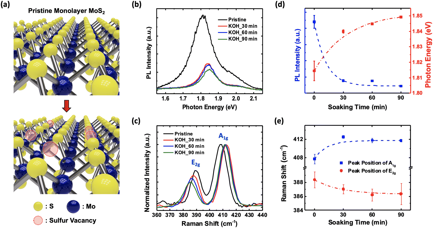 | ||
| Fig. 1 (a) Schematic illustrations of the pristine and defect-containing monolayer MoS2 that contains S-vacancies indicated by red dashed circles. (b and c) Photoluminescence (PL; b) and Raman (c) spectra of monolayer MoS2 treated with KOH for varying soaking times. (d) PL intensity and photon energy of the A exciton as a function of soaking time, showing a decrease in intensity (blue squares) and a blue shift (red dots), respectively, with increasing soaking time. (e) Raman shift as a function of soaking time, displaying the redshifting of the E2g mode and the blueshifting of the A1g mode. The error bars for three samples are shown in (d) and (e). | ||
To evaluate the percentage of S-vacancies in the KOH-treated MoS2 at various soaking times, we exhibit the evolution of the XPS spectrum in the Mo 3d (left panel) and S 2p (right panel) regions, recorded from pristine MoS2 (bottom panel) to the 90 minute-treated (top panel) samples as demonstrated in Fig. 2a. The additional peaks of Mo 3d3/2 and Mo 3d5/2 that appear at slightly lower binding energy values for the 90 minute treatment (top panel) correspond to the defect-containing MoS2 with S-vacancies.32–34 For the semiquantitative analysis of the S/Mo ratio, the XPS spectra are fitted with Lorentzian functions to acquire the area underneath the curves and the S/Mo ratio is normalized to 2, assuming that the S-vacancy in pristine MoS2 is negligible. By following the equation proposed by Bertolazzi et al.,24 the S-vacancy (VS) amount can be expressed as VS = 1 − r/2, where r is the S/Mo ratio. Fig. 2b exhibits a decrease in the normalized S/Mo ratio (left y-axis) and an increase in VS (right y-axis) with increasing soaking time. With these observed relationships, it can be said that, in Fig. 2c, the peak positions of both Mo 3d5/2 and S 2p3/2 shift to lower binding energies with an increasing amount of S-vacancies, resulting in metallic-like behavior.22 Accordingly, to further verify whether the aforementioned defect-induced phenomena also exist in the other two defect-engineered techniques, we also performed XPS experiments on the electron-beam-bombarded MoS2. After testing several electron beam bombardment conditions (as displayed in Fig. S2, ESI†), we irradiated monolayer MoS2 at varying dosages under a fixed electron acceleration voltage (Vacc = 15 kV) and current (I = 0.49 nA) as presented in Fig. S3 of the ESI.† The XPS results of the electron-beam-bombarded MoS2 are consistent with the results observed in the chemically-treated MoS2, wherein a decreasing normalized S/Mo ratio is accompanied by a lowering binding energy as the e-beam dosage is increased (more details can be seen in Fig. S4, ESI†).
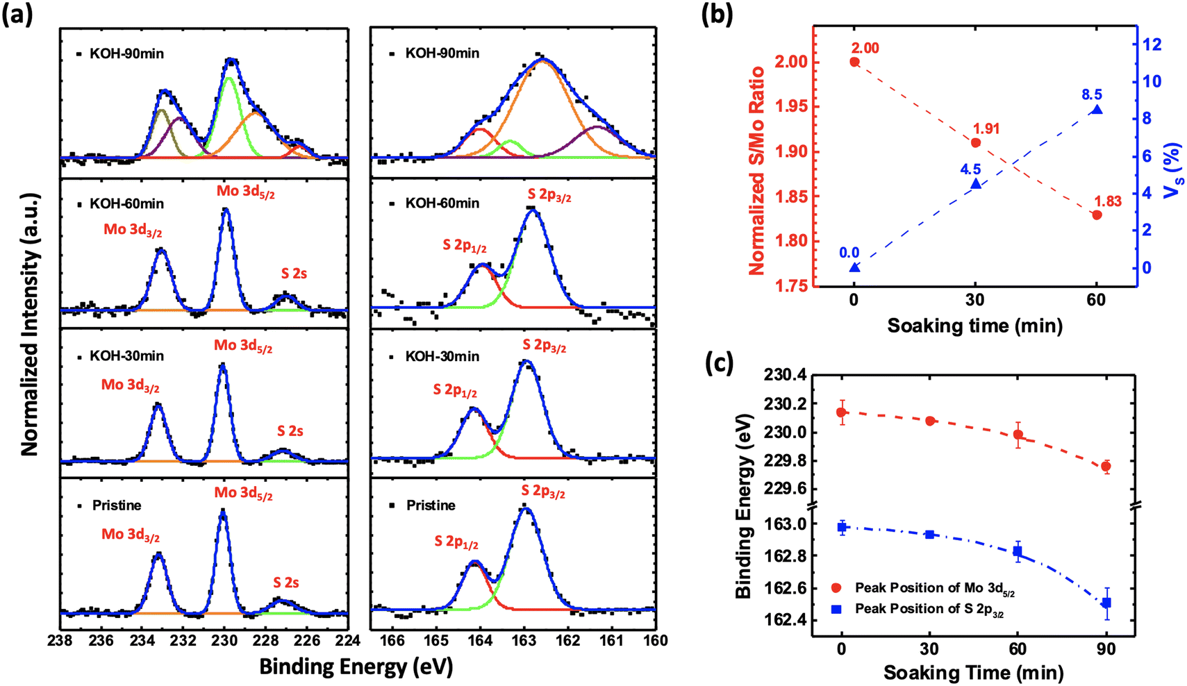 | ||
| Fig. 2 (a) X-ray photoemission spectroscopy (XPS) of Mo 3d (left panel) and S 2p (right panel) at various KOH soaking times. (b) Normalized S/Mo ratio and S-vacancy (VS) as a function of soaking time showing an increasing percentage of VS with increasing soaking time. (c) Peak positions of Mo 3d5/2 and S 2p3/2 shift to lower binding energy values with increasing soaking time. | ||
Based on the aforementioned results that include PL, Raman and XPS, defect-engineered MoS2 FETs with an appropriate amount of S-vacancies can be controlled and adopted to observe NDR behavior using either chemical or physical treatments. Fig. 3a–c present the Id–Vg characteristics of three MoS2 FET devices, which are chemically treated with KOH in 0, 15 and 30 minute durations, respectively, corresponding to S-vacancies from 0 to 4.5%. The optical microscope (OM) images of the measured devices are shown in the insets. The Id–Vg curves progressively become less gate dependent when the duration of the treatment is lengthened, indicating a transition from semiconducting to metallic-like properties. This result can be attributed to the defect states induced by the S-vacancies, which may shift the Fermi level toward the conduction band edge, resulting in metallic-like behavior.35,36 Accordingly, Fig. 3d–f display the corresponding Id–Vg characteristics, respectively, where the NDR effect can be seen clearly in Fig. 3f. It turns out that with a specific amount of S-vacancies (∼4.5%), similar results can also be observed in another 30 minute KOH-treated device presented in Fig. S5 (ESI†). The inset shown in Fig. 3f displays the shifting of the NDR peak positions, which is represented by the correlating bias voltage versus the applied gate voltage. It shows the linear dependence of the NDR peak positions to the gate voltage in the range of −60 V to + 40 V. The gate voltage could possibly shift the Fermi level and align it with the defect/quantum states, causing more tunneling electrons, while the increasing bias voltage may generate more diffusing holes. Consequently, the competition between electrons and holes could result in a shifting of the NDR peak position with increasing Vg.14,17,37 To prove that the S-vacancies in defect-containing MoS2 could result in defect states that can further affect the device's electron transport, we also performed electrical measurements on devices bombarded with different electron beam dosages and observed the resulting NDR behavior at a dosage of ∼5 × 10⁵ μC cm−2, which corresponds to VS ≈ 5% (determined from Fig. S4b, ESI†), as demonstrated in Fig. S6 (ESI†). However, the electrical signal becomes noisy due to the severe damage caused by the physical electron beam bombardment.
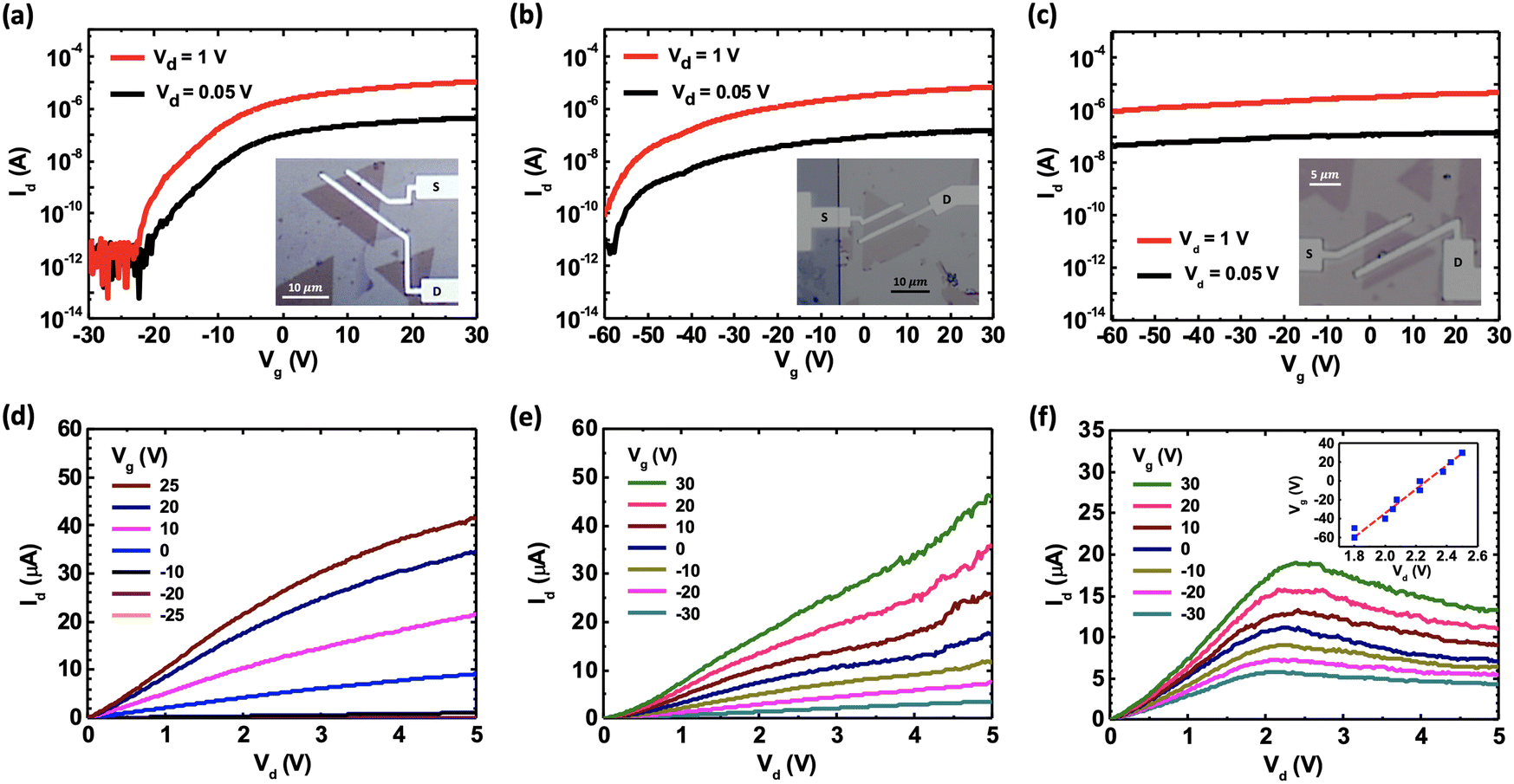 | ||
| Fig. 3 (a–c) Id–Vg characteristics of the MoS2 FET devices showing an evolution from semiconducting to metallic-like behavior with increasing KOH soaking time (0, 15 and 30 minutes, respectively). The insets show the OM images of the respective measured devices. (d–f) Corresponding Id–Vg characteristics demonstrating typical n-type semiconducting behavior. The NDR effect appears in the metallic-like MoS2 device as shown in (f), in which the inset displays the peak positions, represented by their corresponding bias voltage versus gate voltage showing a linear correlation. | ||
In order to minimize the noisy signal caused by the damage caused by the electron beam bombardment, using as-grown monolayer MoS2 with specific amounts of S-vacancies is an appropriate method to achieve stable NDR behavior. We thus synthesized such MoS2 flakes with a particular range of S/Mo ratios using the CVD method under low S supply conditions.38 Accordingly, the as-grown monolayer MoS2 samples with different amounts of S-vacancies, from ∼1% to ∼6%, along with their corresponding XPS results are shown in Fig. S7 (ESI†). Based on the aforementioned results of NDR behavior under the specified S-vacancy conditions, we intentionally fabricated such a MoS2 device with VS ≈ 5%, which was precisely determined through its XPS data shown in Fig. S8 (ESI†). In this device, the observation of NDR can be seen in the Id–Vg curves at different gate voltages without light illumination, as shown in Fig. 4a, while a clearer NDR performance is perceived at a fixed gate voltage Vg = +10 V with different light illumination power values as presented in Fig. 4b. A larger peak to valley ratio is observed since more majority carriers can be induced in the n-type monolayer MoS2 at either Vg = +10 V or at higher light illumination powers. More details of the device's electrical characteristics at different light power values and gate voltages can be seen in Fig. S9 (ESI†). Additionally, another as-grown MoS2 FET with VS ≈ 4.5%, identically confirmed by XPS data, also exhibits NDR behavior, as presented in Fig. S10 (ESI†). Consequently, by growing to achieve a certain range of S-vacancies (∼5 ± 0.5%), the NDR behavior can be reproduced in another MoS2 device, as displayed in Fig. S11 (ESI†). Since the competition between the field-dependent carrier density and the drift velocity determines whether or not the NDR can be observed, we speculate that the defect states at the interface between MoS2 and the electrodes affect the contact resistance, which could further dominate the tunneling mechanism.14,39 However, the hugely different current level appearing in the two types of device, namely the KOH-treated MoS2 and the as-grown MoS2, which correspond to μA and pA current levels, respectively, is probably due to either the channel resistance or contact issues. It is obvious that the devices with a shorter channel length of ∼2 μm have a higher current level, as shown in Fig. 3a–c, than that with a longer channel length of ∼65 μm, as presented in Fig. 4a. Furthermore, according to ref. 40 and our recent experimental results, using semimetallic bismuth (Bi) instead of titanium (Ti) as the buffer layer of the electrodes can achieve almost ohmic contact behavior. Therefore, we believe that the devices designed and fabricated with the shorter channel length and Bi-MoS2 contacts can help to reach a higher current level for approaching the requirement of real applications.
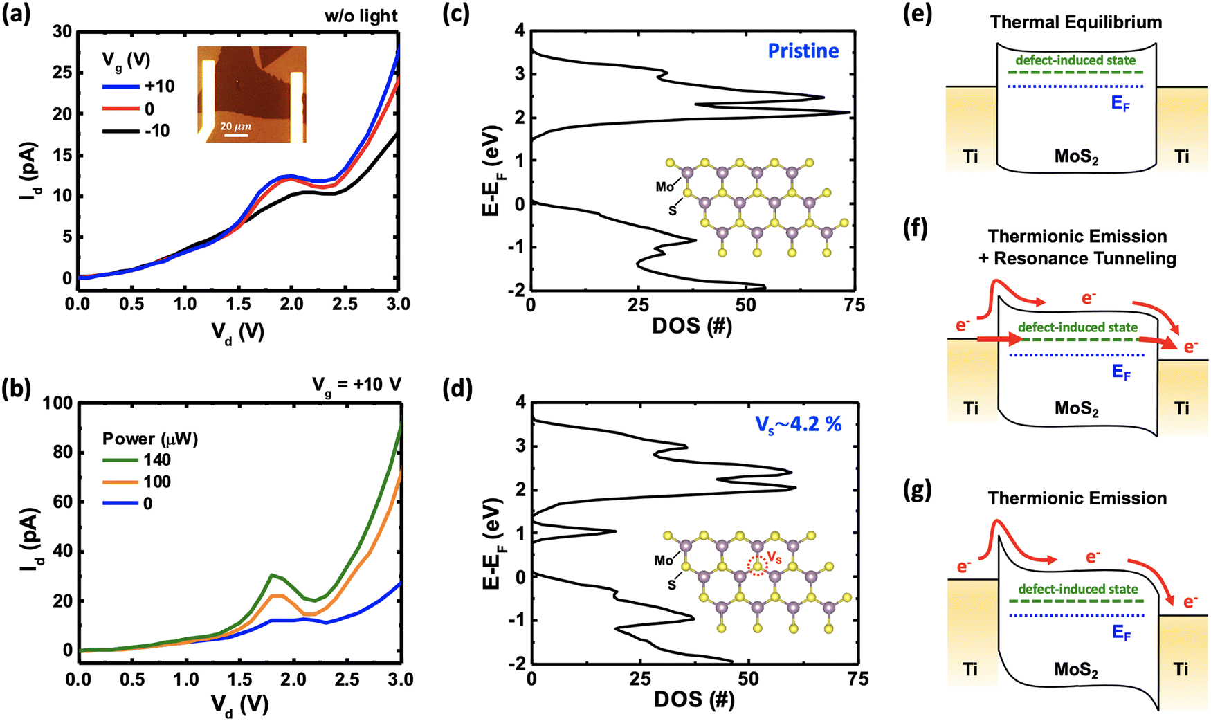 | ||
| Fig. 4 (a) Id–Vd curves at different gate voltages without light illumination. The inset presents the OM image of the measured device. (b) Id–Vd curves illuminated with different light power values at a fixed gate voltage Vg = +10 V. (c and d) Density of states (DOS) of pristine monolayer MoS2 and that with VS ≈ 4.2%, respectively. (e–g) Schematics of band diagrams for different stages of the NDR mechanism. | ||
In order to figure out the possible mechanism, the density of states (DOS) of monolayer MoS2 with S-vacancies is evaluated and a density-functional theory (DFT) simulation is performed using the Vienna ab initio simulation package (VASP).41,42Fig. 4c and d present the simulated DOS of monolayer MoS2 for the pristine sample and that with VS ≈ 4.2%, respectively, in which an additional defect-induced DOS can clearly be seen in the band gap as illustrated in Fig. 4d. A similar defect-induced DOS is obtained for VS from ∼4 to 6%, and it could be responsible for the observation of the NDR behavior. More details about the simulated DOS of MoS2 from pristine condition up to that with VS ≈ 12.6% are presented in Fig. S12 (ESI†), wherein the energy bands move toward to the Fermi level and the number of defect states increases in the bandgap with increasing S-vacancies.30 Consequently, the increasing number of defect states helps more electrons to tunnel through the barrier causing the defect-containing MoS2 FETs to exhibit metallic-like properties. To clearly understand the potential mechanism for NDR behavior, the band diagrams are proposed as demonstrated in Fig. 4e–g. Fig. 4e is the band diagram at thermal equilibrium conditions for MoS2 with an appropriate number of S-vacancies contacted with the metal of Ti, in which an additional defect-induced state is located in the band gap. When a small bias voltage (Vd) is applied to the device with a suitable gate voltage (Vg), the defect-induced state will be aligned to the Fermi level of Ti. Subsequently, the current (Id) will increase due to both the thermionic emission and resonance tunneling mechanisms as presented in Fig. 4f. However, if the bias voltage (Vd) is increased slightly further, the defect-induced state is not aligned with the Fermi level of Ti, and only thermionic emission contributes to the electron transport as demonstrated in Fig. 4g, leading to the decreased current forming an NDR peak as shown in Fig. 4a and b. Therefore, with an appropriate amount of S-vacancies, the NDR behavior can be theoretically predicted and experimentally observed.
Conclusions
The NDR effect is observed in monolayer MoS2 FETs via defect engineering approaches, including chemical treatment with KOH, electron beam bombardment, and as-grown MoS2 with a specific amount of S-vacancies. Based on systematic studies for the correlation of the S-vacancies with both the electrical characteristics and spectroscopic analysis (PL, Raman and XPS), the NDR effect has been clearly observed at room temperature in defect-engineered monolayer MoS2 FETs with VS ≈ 5 ± 0.5%. Moreover, stable NDR behavior can also be effectively modulated via the gate electric field and light intensity. We believe that these results may provide an alternative route to develop more electronic applications based on defect-containing monolayer TMDs in the future.Methods
Material synthesis
MoS2 was synthesized on a sapphire substrate via the chemical vapor deposition (CVD) method at 190 °C. Initially, molybdenum trioxide (MoO3) powder was placed in a quartz boat located at the heating zone center of the furnace, and the sapphire substrate was placed next to the quartz boat. Sulfur (S) powder was prepared in another quartz boat at the upstream side of the furnace. An argon gas flow was then used to bring both the S and MoO3 vapors towards the sapphire substrate.Device fabrication
After synthesizing the monolayer MoS2, PMMA was coated on the MoS2 film at a spin speed of 4000 rpm for 55 seconds. The sapphire/MoS2/PMMA substrate was subsequently immersed in an ammonia solution for one to two hours to separate the MoS2/PMMA film from the sapphire substrate.43,44 After transferring the MoS2/PMMA film onto the Si/SiO2 substrate, the PMMA protection layer was removed using acetone. The sample was then immersed in an N-methyl-2-pyrrolidone solution for wet cleaning to remove residues or contamination on the MoS2 surface.45 A new layer of PMMA was coated on the Si/SiO2/MoS2 substrate at a spin speed of 4000 rpm for 55 seconds for the e-beam lithography process. Finally, the Ti (20 nm)/Au (50 nm) electrodes were deposited using a thermal evaporator.XPS experiments
The XPS data for KOH-treated MoS2 were recorded using a Thermo Fisher Scientific Theta Probe at the Taiwan Semiconductor Research Institute. Monochromatic anode X-rays (1486.6 eV photon energy) were focused down to ∼15 μm. Additionally, the XPS data for e-beam bombarded MoS2 and as-grown MoS2 were obtained using the scanning photoelectron microscopy (SPEM) endstation at beamline 09A1 of the National Synchrotron Radiation Research Center's Taiwan Light Source. Monochromatic soft X-rays (400 eV photon energy) were focused down to ∼200 nm using Fresnel-zone-plate-based focusing optics. By raster-scanning the sample relative to the focused beam and collecting the photoelectrons, SPEM can produce the surface elemental distribution image. Based on the SPEM image, we moved the focused beam to a specific location of interest to record the high-resolution photoelectron spectra of the microscopic area. All samples were annealed at about 450 K for 8 hours prior to SPEM measurement. The measurements were recorded under ultra-high vacuum (UHV) conditions near 300 K.Density functional theory simulations
The density of states (DOS) for monolayer MoS2 with different S-vacancy concentrations was investigated through density-functional theory (DFT) simulations using the Vienna ab initio simulation package (VASP). A 3 × 4 × 1 supercell of MoS2 with a vacuum layer of 18 Å was used as a good approximation for the isolated 2D slab. An 11 × 11 × 1 k-points and a 500 eV cut-off energy were selected in all supercells. The relaxed lattice constant of monolayer MoS2 without sulfur vacancies is 3.18 Å. The DOS of MoS2 with sulfur vacancies ranging from 4.2% to 12.6% was then calculated by removing one to three sulfur atoms in the 3 × 4 × 1 supercell.Author contributions
In this work, W.-H. Chang, T. H. Yang and S.-T. Yang performed the device fabrication and data analysis. The XPS experiments conducted in TSRI were supported by J.-H. Chen and K.-S. Li. The XPS experiments conducted at the NSRRC were supported by C.-I. Lu, S.-H. Hsieh and C.-H. Chen. The DFT simulations were supported by C.-P. Lin and T.-H. Hou. The manuscript was prepared and reviewed by W.-H. Chang, C.-I. Lu, K. B. Simbulan and T.-H. Lu. This project was conceived and led by Y.-W. Lan.Conflicts of interest
There are no conflicts of interest to declare.Acknowledgements
The authors thank members of TLS 09A1 at the National Synchrotron Radiation Research Center's Taiwan Light Source for their suggestions on the analysis of XPS data and earlier test measurements. We thank Mr. Kui-Hon Ou Yang and Prof. Minn-Tsong Lin at National Taiwan University for their suggestions and help with conducting the XPS experiments. We also thank members of the Taiwan Semiconductor Research Institute for their help with XPS measurements. This work was supported by the Ministry of Science and Technology, Taiwan under contract no. MOST 108-2112-M-003-010-MY3 and MOST 111-2119-M-008-003-MBK.References
- L. Esaki, Phys. Rev., 1958, 109, 603–604 CrossRef CAS.
- L. Esaki and R. Tsu, IBM J. Res. Dev., 1970, 14, 61–65 CAS.
- M. Herzig, M. Weiher, A. Ascoli, R. Tetzlaff, T. Mikolajick and S. Slesazeck, J. Phys. D: Appl. Phys., 2019, 52, 325104 CrossRef CAS.
- S. Chen, P. B. Griffin and J. D. Plummer, IEEE Trans. Electron Devices, 2009, 56, 634–640 CAS.
- S. Wang, A. Pan, C. Grezes, P. K. Amiri, K. L. Wang, C. O. Chui and P. Gupta, IEEE Trans. Electron Devices, 2017, 64, 4084–4090 CAS.
- K.-H. Kim, H.-Y. Park, J. Shim, G. Shin, M. Andreev, J. Koo, G. Yoo, K. Jung, K. Heo, Y. Lee, H.-Y. Yu, K. R. Kim, J. H. Cho, S. Lee and J.-H. Park, Nanoscale Horiz., 2020, 5, 654–662 RSC.
- R. J. Hwu, A. Djuandi and S. C. Lee, IEEE Trans. Microwave Theory Tech., 1993, 41, 890–893 CrossRef CAS.
- V. Ulansky, A. Raza and H. Oun, Electronics, 2019, 8, 409 CrossRef.
- F. Léonard and J. Tersoff, Phys. Rev. Lett., 2000, 85, 4767–4770 CrossRef PubMed.
- M. Rinkiö, A. Johansson, V. Kotimäki and P. Törmä, ACS Nano, 2010, 4, 3356–3362 CrossRef PubMed.
- Y. Wu, D. B. Farmer, W. Zhu, S.-J. Han, C. D. Dimitrakopoulos, A. A. Bol, P. Avouris and Y.-M. Lin, ACS Nano, 2012, 6, 2610–2616 CrossRef CAS PubMed.
- P. Sharma, L. S. Bernard, A. Bazigos, A. Magrez and A. M. Ionescu, ACS Nano, 2015, 9, 620–625 CrossRef CAS PubMed.
- S. Rathi, I. Lee, M. Kang, D. Lim, Y. Lee, S. Yamacli, H.-I. Joh, S. Kim, S.-W. Kim, S. J. Yun, S. Choi and G.-H. Kim, Sci. Rep., 2018, 8, 7144 CrossRef PubMed.
- S.-T. Yang, T. H. Yang, C.-I. Lu, W.-H. Chang, K. B. Simbulan and Y.-W. Lan, Carbon, 2021, 176, 440–445 CrossRef CAS.
- N. T. Duong, S. Bang, S. M. Lee, D. X. Dang, D. H. Kuem, J. Lee, M. S. Jeong and S. C. Lim, Nanoscale, 2018, 10, 12322–12329 RSC.
- T. Roy, M. Tosun, X. Cao, H. Fang, D.-H. Lien, P. Zhao, Y.-Z. Chen, Y.-L. Chueh, J. Guo and A. Javey, ACS Nano, 2015, 9, 2071–2079 CrossRef CAS PubMed.
- C.-Y. Lin, X. Zhu, S.-H. Tsai, S.-P. Tsai, S. Lei, Y. Shi, L.-J. Li, S.-J. Huang, W.-F. Wu, W.-K. Yeh, Y.-K. Su, K. L. Wang and Y.-W. Lan, ACS Nano, 2017, 11, 11015–11023 CrossRef CAS PubMed.
- Y.-C. Lin, R. K. Ghosh, R. Addou, N. Lu, S. M. Eichfeld, H. Zhu, M.-Y. Li, X. Peng, M. J. Kim, L.-J. Li, R. M. Wallace, S. Datta and J. A. Robinson, Nat. Commun., 2015, 6, 7311 CrossRef CAS PubMed.
- A. Sengupta and S. Mahapatra, J. Appl. Phys., 2013, 114, 194513 CrossRef.
- K. Cho, M. Min, T.-Y. Kim, H. Jeong, J. Pak, J.-K. Kim, J. Jang, S. J. Yun, Y. H. Lee, W.-K. Hong and T. Lee, ACS Nano, 2015, 9, 8044–8053 CrossRef CAS PubMed.
- M. R. Islam, N. Kang, U. Bhanu, H. P. Paudel, M. Erementchouk, L. Tetard, M. N. Leuenberger and S. I. Khondaker, Nanoscale, 2014, 6, 10033–10039 RSC.
- Q. Ma, P. M. Odenthal, J. Mann, D. Le, C. S. Wang, Y. Zhu, T. Chen, D. Sun, K. Yamaguchi, T. Tran, M. Wurch, J. L. McKinley, J. Wyrick, K. Magnone, T. F. Heinz, T. S. Rahman, R. Kawakami and L. Bartels, J. Phys.: Condens. Matter, 2013, 25, 252201 CrossRef PubMed.
- S. Mignuzzi, A. J. Pollard, N. Bonini, B. Brennan, I. S. Gilmore, M. A. Pimenta, D. Richards and D. Roy, Phys. Rev. B: Condens. Matter Mater. Phys., 2015, 91, 195411 CrossRef.
- S. Bertolazzi, S. Bonacchi, G. Nan, A. Pershin, D. Beljonne and P. Samorì, Adv. Mater., 2017, 29, 1606760 CrossRef PubMed.
- H.-P. Komsa, J. Kotakoski, S. Kurasch, O. Lehtinen, U. Kaiser and A. V. Krasheninnikov, Phys. Rev. Lett., 2012, 109, 035503 CrossRef PubMed.
- W. M. Parkin, A. Balan, L. Liang, P. M. Das, M. Lamparski, C. H. Naylor, J. A. Rodríguez-Manzo, A. T. C. Johnson, V. Meunier and M. Drndić, ACS Nano, 2016, 10, 4134–4142 CrossRef CAS PubMed.
- E. Scalise, M. Houssa, G. Pourtois, V. V. Afanas’ev and A. Stesmans, Phys. E, 2014, 56, 416–421 CrossRef CAS.
- H. Li, Q. Zhang, C. C. R. Yap, B. K. Tay, T. H. T. Edwin, A. Olivier and D. Baillargeat, Adv. Funct. Mater., 2012, 22, 1385–1390 CrossRef CAS.
- C. Rice, R. J. Young, R. Zan, U. Bangert, D. Wolverson, T. Georgiou, R. Jalil and K. S. Novoselov, Phys. Rev. B: Condens. Matter Mater. Phys., 2013, 87, 081307 CrossRef.
- H. Li, C. Tsai, A. L. Koh, L. Cai, A. W. Contryman, A. H. Fragapane, J. Zhao, H. S. Han, H. C. Manoharan, F. Abild-Pedersen, J. K. Nørskov and X. Zheng, Nat. Mater., 2016, 15, 48–53 CrossRef CAS PubMed.
- B. Chakraborty, A. Bera, D. V. S. Muthu, S. Bhowmick, U. V. Waghmare and A. K. Sood, Phys. Rev. B: Condens. Matter Mater. Phys., 2012, 85, 161403 CrossRef.
- I. S. Kim, V. K. Sangwan, D. Jariwala, J. D. Wood, S. Park, K.-S. Chen, F. Shi, F. Ruiz-Zepeda, A. Ponce, M. Jose-Yacaman, V. P. Dravid, T. J. Marks, M. C. Hersam and L. J. Lauhon, ACS Nano, 2014, 8, 10551–10558 CrossRef CAS PubMed.
- K. C. Kwon, C. Kim, Q. V. Le, S. Gim, J.-M. Jeon, J. Y. Ham, J.-L. Lee, H. W. Jang and S. Y. Kim, ACS Nano, 2015, 9, 4146–4155 CrossRef CAS PubMed.
- D. M. Sim, M. Kim, S. Yim, M.-J. Choi, J. Choi, S. Yoo and Y. S. Jung, ACS Nano, 2015, 9, 12115–12123 CrossRef CAS.
- S. McDonnell, R. Addou, C. Buie, R. M. Wallace and C. L. Hinkle, ACS Nano, 2014, 8, 2880–2888 CrossRef CAS PubMed.
- C.-P. Lin, P.-C. Chen, J.-H. Huang, C.-T. Lin, D. Wang, W.-T. Lin, C.-C. Cheng, C.-J. Su, Y.-W. Lan and T.-H. Hou, ACS Appl. Electron. Mater., 2019, 1, 684–691 CrossRef CAS.
- G. P. Lansbergen, R. Rahman, C. J. Wellard, I. Woo, J. Caro, N. Collaert, S. Biesemans, G. Klimeck, L. C. L. Hollenberg and S. Rogge, Nat. Phys., 2008, 4, 656–661 Search PubMed.
- J. Chen, X. Zhao, G. Grinblat, Z. Chen, S. J. R. Tan, W. Fu, Z. Ding, I. Abdelwahab, Y. Li, D. Geng, Y. Liu, K. Leng, B. Liu, W. Liu, W. Tang, S. A. Maier, S. J. Pennycook and K. P. Loh, Adv. Mater., 2018, 30, 1704674 CrossRef.
- P. X. Tran, J. Electron. Mater., 2018, 47, 5905–5912 CrossRef CAS.
- P.-C. Shen, C. Su, Y. Lin, A.-S. Chou, C.-C. Cheng, J.-H. Park, M.-H. Chiu, A.-Y. Lu, H.-L. Tang, M. M. Tavakoli, G. Pitner, X. Ji, Z. Cai, N. Mao, J. Wang, V. Tung, J. Li, J. Bokor, A. Zettl, C.-I. Wu, T. Palacios, L.-J. Li and J. Kong, Nature, 2021, 593, 211–217 CrossRef CAS PubMed.
- J. Hafner, J. Comput. Chem., 2008, 29, 2044–2078 CrossRef CAS.
- Y. Tsai and Y. Li, IEEE Trans. Electron Devices, 2018, 65, 733–738 CAS.
- C.-P. Lin, P.-S. Liu, L. Lyu, M. Li, C.-C. Cheng, T.-H. Lee, W. Chang, L. Li and T. Hou, N-type Doping Effect of Transferred MoS2 and WSe2 Monolayer, Extended Abstracts of the 2015 International Conference on Solid State Devices and Materials, Sapporo, 2015, pp. 642–643.
- K. B. C. Simbulan, P. C. Chen, Y. Y. Lin and Y. W. Lan, J. Visualized Exp., 2018, 138, e57885 Search PubMed.
- P.-C. Chen, C.-P. Lin, C.-J. Hong, C.-H. Yang, Y.-Y. Lin, M.-Y. Li, L.-J. Li, T.-Y. Yu, C.-J. Su, K.-S. Li, Y.-L. Zhong, T.-H. Hou and Y.-W. Lan, Nano Res., 2019, 12, 303–308 CrossRef CAS.
Footnote |
| † Electronic supplementary information (ESI) available. See DOI: https://doi.org/10.1039/d2nh00396a |
| This journal is © The Royal Society of Chemistry 2022 |