
 Open Access Article
 This Open Access Article is licensed under a
 Creative Commons Attribution 3.0 Unported Licence
Atomic layer deposition of PbCl2, PbBr2 and mixed lead halide (Cl, Br, I) PbXnY2−n thin films†
Georgi
Popov
 *a,
Goran
Bačić
b,
Charlotte
Van Dijck
a,
Laura S.
Junkers
a,
Alexander
Weiß
a,
Miika
Mattinen
a,
Anton
Vihervaara
a,
Mykhailo
Chundak
a,
Pasi
Jalkanen
c,
Kenichiro
Mizohata
c,
Markku
Leskelä
a,
Jason D.
Masuda
d,
Seán T.
Barry
b,
Mikko
Ritala
*a and
Marianna
Kemell
a
*a,
Goran
Bačić
b,
Charlotte
Van Dijck
a,
Laura S.
Junkers
a,
Alexander
Weiß
a,
Miika
Mattinen
a,
Anton
Vihervaara
a,
Mykhailo
Chundak
a,
Pasi
Jalkanen
c,
Kenichiro
Mizohata
c,
Markku
Leskelä
a,
Jason D.
Masuda
d,
Seán T.
Barry
b,
Mikko
Ritala
*a and
Marianna
Kemell
a
aDepartment of Chemistry, University of Helsinki, P. O. Box 55, FI-00014 Helsinki, Finland. E-mail: georgi.popov@helsinki.fi; mikko.ritala@helsinki.fi
bDepartment of Chemistry, Carleton University, 1125 Colonel By Drive, Ottawa, Ontario K1S 5B6, Canada
cDepartment of Physics, University of Helsinki, P. O. Box 43, FI-00014 Helsinki, Finland
dDepartment of Chemistry, Saint Mary's University, 923 Robie Street, Halifax, Nova Scotia B3H 3C3, Canada
First published on 16th September 2022
Abstract
Atomic layer deposition offers outstanding film uniformity and conformality on substrates with high aspect ratio features. These qualities are essential for mixed-halide perovskite films applied in tandem solar cells, transistors and light-emitting diodes. The optical and electronic properties of mixed-halide perovskites can be adjusted by adjusting the ratios of different halides. So far ALD is only capable of depositing iodine-based halide perovskites whereas other halide processes are lacking. We describe six new low temperature (≤100 °C) ALD processes for PbCl2 and PbBr2 that are crucial steps for the deposition of mixed-halide perovskites with ALD. Lead bis[bis(trimethylsilyl)amide]–GaCl3 and –TiBr4 processes yield the purest, crystalline, uniform and conformal films of PbCl2 and PbBr2 respectively. We show that these two processes in combination with a PbI2 process from the literature deposit mixed lead halide films. The four less optimal processes revealed that reaction by-products in lead halide deposition processes may cause film etching or incorporate themselves into the film.
1. Introduction
This work describes new atomic layer deposition (ALD) processes for lead chloride and bromide thin films. These halide thin films act as precursors for halide perovskite thin films.1 Halide perovskites are a group of compounds with a crystal structure similar to the mineral perovskite and the general formula ABX3, where A is typically an amine or caesium, B is lead or tin, and X is a halide, namely chloride, bromide or most commonly iodide. Halide perovskites possess remarkable optoelectronic properties and have rapidly established themselves as the next generation photovoltaic materials.2,3 However, the potential of halide perovskites is not limited to photovoltaics.4 At present, they display impressive performance in many devices5 including light-emitting diodes (LEDs),6 X-ray scintillators7 and transistors.8We believe that in certain applications ALD can become the method of choice for depositing halide perovskites. ALD offers uniformity and conformality that other deposition methods struggle to achieve. These advantages allow ALD to excel in applications, such as microelectronics, that rely on complex high aspect ratio structures.9 In the halide perovskite case, high aspect ratio structures either enable key functionality of the device or enhance performance.5
Previously we have developed ALD processes for PbI2![[thin space (1/6-em)]](https://www.rsc.org/images/entities/char_2009.gif) 10 and CsI11 based on metal bis(trimethylsilyl)amides (btsa) and tin tetraiodide. In these processes a ligand exchange reaction between the metal (btsa) and SnI4 yields the desired metal iodide and volatile heteroleptic tin by-products (Sn(btsa)xI4−x). The PbI2 and CsI processes also allowed us to deposit thin films of CH3NH3PbI3 (MAPbI3)10 and CsPbI3.11 However, most halide perovskite applications rely on mixed halide perovskites i.e., partial substitution of ions in the perovskite composition, for example substitution of iodine with bromine or chlorine in MAPbI3.5–8,12 Currently (June 2022), to our knowledge, our iodide ALD processes,10,11 the work of Natarajan et al. on copper chloride13 as well as the recent work of Vagott et al. on PbI214 constitute the entirety of existing literature on direct ALD of metal chlorides and iodides.15 No metal bromide ALD processes have been reported. This work expands the range of metal halides that can be deposited with ALD to lead chloride and bromide.
10 and CsI11 based on metal bis(trimethylsilyl)amides (btsa) and tin tetraiodide. In these processes a ligand exchange reaction between the metal (btsa) and SnI4 yields the desired metal iodide and volatile heteroleptic tin by-products (Sn(btsa)xI4−x). The PbI2 and CsI processes also allowed us to deposit thin films of CH3NH3PbI3 (MAPbI3)10 and CsPbI3.11 However, most halide perovskite applications rely on mixed halide perovskites i.e., partial substitution of ions in the perovskite composition, for example substitution of iodine with bromine or chlorine in MAPbI3.5–8,12 Currently (June 2022), to our knowledge, our iodide ALD processes,10,11 the work of Natarajan et al. on copper chloride13 as well as the recent work of Vagott et al. on PbI214 constitute the entirety of existing literature on direct ALD of metal chlorides and iodides.15 No metal bromide ALD processes have been reported. This work expands the range of metal halides that can be deposited with ALD to lead chloride and bromide.
We hypothesized that the chemistry that we used for iodides is straightforward to extend to chlorides and bromides, but we encountered a number of challenges and a chloride process required a previously unthought halide precursor. The use of metal halide as a halide precursor originates from the metal fluoride ALD chemistry developed by Pilvi et al. who used TiF4 and TaF5 as fluorine precursors. In the fluoride ALD process the use of metal fluorides as fluorine sources allows to avoid the use of anhydrous HF gas. In our case, the lack of commercial availability of the anhydrous HCl, HBr and HI gases compelled us to investigate alternatives like the use of metal halides as halide precursors. The technical challenges we faced originated from the halide precursors. Tin(IV) iodide is a convenient iodide precursor for the metal iodide deposition, but the analogous chloride and bromide had either performance or delivery issues. To circumvent these issues, we studied alternative halide precursors: titanium(IV) halides and gallium(III) chloride as well as an alternative lead precursor: bis[lead(II) N,N′-di-tert-butyl-1,1-dimethylsilanediamide] ([Pb(gem)]2). Here, we describe these studies and their outcome: ALD processes for PbCl2 and PbBr2. Both processes use Pb(btsa)2 as the lead precursor, whereas GaCl3 and TiBr4 are the respective halide precursors.
2. Results and discussion
Table 1 shows key characteristics of the processes we studied. Pb(btsa)2 combined with either GaCl3 or TiBr4 result in good processes whereas the other chemistries either lack key ALD characteristics or deposit thin films with undesired properties.| Material | Lead precursor | Halide precursor | Crystallinity | Metal impurities | Refractive indexa | Process characteristics |
|---|---|---|---|---|---|---|
| a At 580 nm. | ||||||
| PbCl2 | Pb(btsa)2 | SnCl4 | Crystalline | <0.1 at% Sn | 2.3 | No saturation, etching |
| TiCl4 | Crystalline | 11.2 at% Ti | 1.9 | Saturation with respect to the halide precursor but not the metal precursor | ||
| GaCl3 | Crystalline | 1.0 at% Ga | 2.2 | Saturation | ||
| (Pb(gem))2 | SnCl4 | Crystalline | 15.9 at% Sn | 1.9 | Saturation | |
| PbBr2 | Pb(btsa)2 | SnBr4 | Amorphous | 7.8 at% Sn | 1.9 | Saturation with respect to the halide precursor but not the metal precursor |
| TiBr4 | Crystalline | 0.5 at% Ti | 2.5 | Saturation | ||
2.1 Pb(btsa)2–SnCl4 process
At 65 °C, Pb(btsa)2 and SnCl4 yielded crystalline and pure PbCl2 (Fig. S1a and b,† refractive index 2.3, literature value 2.316), but the films suffered from severe thickness non-uniformity (Fig. S1c†). Standard deviations in thickness across the substrate (σd) ranged from 14 to 88%. The films were thinner at the precursor inlet edge of the substrate and most uniform films required short pulse durations with no purge in between (Fig. S1d†). Long pulse or purge durations as well as higher deposition temperatures caused an expansion of the thinner region across the substrate and ultimately no deposition at all (Fig. S1e–h†).
Our experimental results suggested that an intermediate product with the formula Sn(btsa)x(Cl)4−x of the reaction between Pb(btsa)2 and SnCl4 was responsible for the etching rather than the precursors themselves. Neither Pb(btsa)2 or SnCl4 pulsed onto an already deposited PbCl2 film (2000 cycles at 65 °C, precursor pulse and purge durations were 1 and 3 s respectively) caused any measurable decrease in the film thickness or change in the thickness profile. Additionally, sublimation of PbCl2 could not explain the etching as other processes can deposit PbCl2 films that are stable inside our reactors up to at least 135 °C. These observations were further supported by a quantum chemical study (vide infra) presented in Section 2.5.
2.2 Pb(btsa)2–TiCl4 process
Because SnCl4 did not yield a good process we turned to TiCl4 as a next possible chloride precursor. Tetrahalides (Cl, Br, I) of tin and titanium have similar structure, size, and properties, although titanium tetrahalides are slightly less volatile than the tin analogues.The thinning effect observed with SnCl4 did not occur in the case of TiCl4. On the contrary the films were thicker at the precursor inlet edge with a visible thickness gradient (σd = 40%). Short pulse and long purge durations as well as a thin ALD Al2O3 underlayer (2 nm) deposited with trimethylaluminum (TMA) and H2O, improved the thickness uniformity (Fig. S2a and d†).
Key ALD characteristics were missing from the Pb(btsa)2 and TiCl4 process. The growth per cycle (GPC) saturated with respect to the TiCl4 pulse and purge durations but not with respect to the Pb(btsa)2 pulse durations (Fig. S2c and d†). At the deposition temperature of 75 °C the thickness increased linearly with the increasing number of deposition cycles (Fig. S2f†). The GPC decreased with increasing deposition temperature (Fig. S2g†).
The films are not pure PbCl2 and are chlorine deficient (Fig. S2h†). Titanium and oxygen are present in significant amounts, whereas carbon and nitrogen are not. Changes in process parameters did not yield any significant changes in film composition. No well-defined grains or grain boundaries are visible with FESEM (Fig. S2b†). XRD reveals PbCl2 reflections (FWHM 0.5° of 2θ) for the 30–80 nm thick films deposited in the 65–110 °C temperature range (Fig. S2i†). The measured refractive index (1.9) does not match that of PbCl2 (2.316).
We speculate that the formation of a ternary chloride, for instance PbTiCl6, along with PbCl2 can explain the impurity and poor crystallinity of the films. The Pb:Ti:O ratio is roughly 1:1:3 if we subtract the PbCl2 part from the composition given in Fig. S2h.† Only PbCl2 reflections are present in the XRD patterns, therefore the oxygen containing part of the film likely consists of one or more of the amorphous phases of PbO, TiO2 and PbTiO3. The oxygen containing part can form when the ternary chloride is exposed to ambient air (eqn (1) and (2)).
| PbTiCl6(s) + 3H2O(g) → PbO(s) + TiO2(s) + 6HCl(g) | (1) |
| PbTiCl6(s) + 3H2O(g) → PbTiO3(s) + 6HCl(g) | (2) |
Literature covers many ternary fluoride II–IV compounds with double ReO3 type (DROT) perovskite structure17 as well as some II–IV chlorides with various structures.18–20 Alternatively, one or more air sensitive and non-volatile Pb and Ti containing by-products can account for the observed oxygen containing composition.
2.3 (Pb(gem))2–SnCl4 process
(Pb(gem))2 is a new precursor for the ALD field. (Pb(gem))2 has excellent thermal stability up to at least 300 °C21 and is more volatile than Pb(btsa)2 (Fig. 1 and Fig. S3†). These properties make (Pb(gem))2 usable in a wide temperature range. Wrackmeyer et al. describe that in solution Pb(gem) and SnCl4 react to form PbCl2 and Sn(gem)Cl2 (eqn (3) and (4)),22 which encouraged us to explore the same chemistry in ALD. We also speculated that avoiding the (btsa) ligand would allow us to circumvent the etching issue in the Pb(btsa)2–SnCl4 process.| Pb(gem) + 2SnCl4 → PbCl2 + (gem)(SnCl3)2 | (3) |
| (gem)(SnCl3)2 → SnCl4 + Sn(gem)Cl2 | (4) |
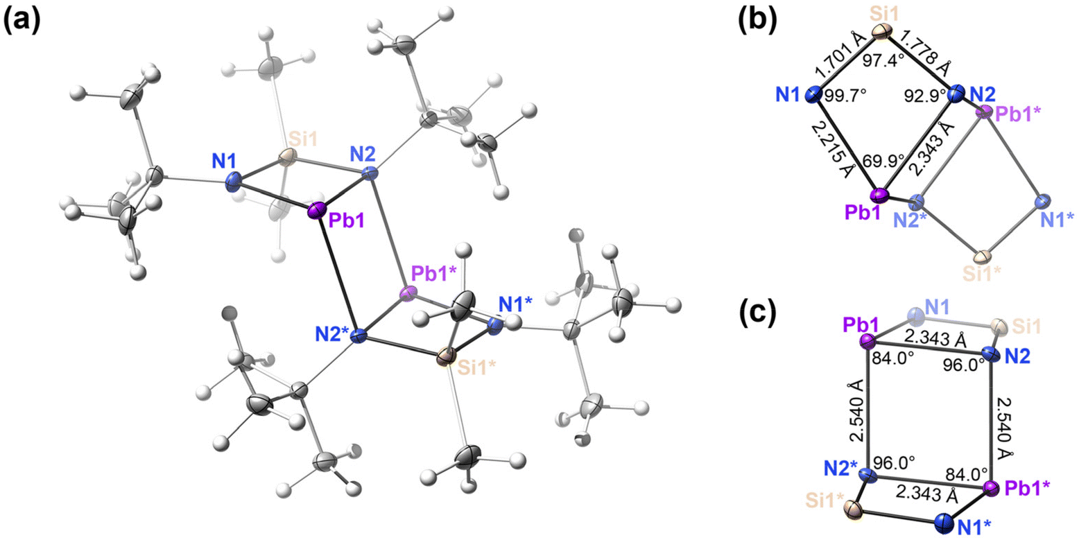 | ||
| Fig. 1 (a) Asymmetric unit of (Pb(gem))2 in the solid state as determined by single-crystal X-ray diffraction (scXRD), (b and c) interatomic distances and angles of the central inorganic ladderane structure with carbons and hydrogens omitted for clarity. Ellipsoids were drawn at the 50% probability isosurface, except hydrogens which were drawn as spheres. | ||
The films deposited with the (Pb(gem))2–SnCl4 process had a visible thickness gradient. The thickness decreased in the direction of the precursor flow (Fig. S4a†). The thickness gradient was observed at all deposition temperatures but varied in steepness. This change in steepness caused notable scatter in the GPC vs. deposition temperature data (Fig. S4c†). Assuming this scatter does not obscure the trend in GPC, the GPC is constant up to 135 °C. No deposition occurs at temperatures above 135 °C. At 85 °C the GPC saturates with respect to both precursor pulse durations but increases with increasing purge duration (Fig. S4d–f†). The film thickness depends linearly on the number of deposition cycles (Fig. S4g†).
The films made from (Pb(gem))2 and SnCl4 contained significant amounts of tin, oxygen, carbon and hydrogen (Fig. S4h†), but the Pb to Cl ratio was nevertheless 1 to 2. The films were amorphous at deposition temperatures below 85 °C, whereas broad (FWHM 1.0° of 2θ) PbCl2 reflections appeared at 85 °C and higher deposition temperatures (Fig. S4i†). FESEM images show small grains embedded in a featureless matrix (Fig. S4b†). The measured refractive index (1.9) differs significantly from the literature value for PbCl2 (2.3, ref. 16).
The composition of the films made with the (Pb(gem))2–SnCl4 process suggests that the source of the impurities is a different one than in the Pb(btsa)2–TiCl4 process. The notable Sn, O, and H contents as well as the Pb to Cl ratio matching stoichiometric PbCl2 may indicate that by-products, which contain the (gem) ligand (see eqn (3) and (4)), are incorporated into the film during deposition. The reason for the by-product incorporation could be their insufficient volatility in the temperature range where the PbCl2 deposition occurs. The oxygen content can be attributed to the reaction of these incorporated by-products with ambient air.
To summarize, (Pb(gem))2 offers many advantages over Pb(btsa)2, such as simpler synthesis, better storage and thermal stability.21,23 But these advantages cannot be exploited when (Pb(gem))2 is paired with SnCl4 to deposit PbCl2. For instance, the remarkable thermal stability which (Pb(gem))2 exhibits up to 300 °C, has no importance since deposition only occurs at temperatures below 135 °C. Furthermore, (Pb(gem))2 and SnCl4 generate non-volatile by-products (eqn (3) and (4)),22 that negatively affect film qualities such as thickness uniformity, purity and crystallinity (Fig. S4a, h and i†). Nevertheless, (Pb(gem))2 could still be a viable alternative for the deposition of lead compounds if paired with co-reactants that do not generate non-volatile by-products.
2.4 Pb(btsa)2–GaCl3 process
We investigated other metal chlorides as possible chlorine precursors because of the issues we observed with SnCl4 and TiCl4. GaCl3 stood out in our literature study. Several studies describe GaCl3 as a volatile gallium precursor that can be used in ALD of gallium compounds.24–26 Reports on GaCl3 reacting with metal bis(trimethylsilyl)amides to form the corresponding metal chloride and volatile by-products were also promising.27–30Delivery of GaCl3 required some creativity. Typically, in our F120 ALD reactors, volatile solids are delivered from open glass boats that are placed inside the reactor and heated to the source temperature. The volatility of GaCl3, however, allowed its delivery at room temperature, i.e. without additional heating. Films deposited with GaCl3 delivered from an open glass boat, that we use for solid precursors, were rough with nonuniform thickness (Fig. S5a†). Despite these detrimental features the gallium content in the films was small (<2 at%, EDS).
We suspected that the poor quality of the films was caused by overdosing of GaCl3 as well as incomplete purging. GaCl3 consumption was thrice as high than the typical precursor consumption in our reactors. Longer purge durations and higher deposition temperature slightly improved the uniformity. Normally the next step would be to lower the precursor source temperature, but GaCl3 was already being delivered without heating. Instead, we attempted to lower GaCl3 dose by limiting its flow out of the glass boat with an orifice. A 7 × 5 mm orifice decreased the thickness non-uniformity (σd) to 26% (Fig. S5b and S6a†). While this improvement was significant, the thickness non-uniformity was still exceeded what we consider acceptable for our flow-type reactors (σd ≤ 5%). Even smaller orifice sizes would, however, imped the loading of solid GaCl3. To overcome this obstacle, we used GaCl3 solution instead of the solid GaCl3. Dissolving GaCl3 allowed it's loading via a syringe and further reduction of the size of the orifice down to 1 mm. Hexane was the solvent of choice, as it is inert towards GaCl3 and evaporates during the reactor pump down, leaving solid GaCl3 in the source boat (Video S1†).
With an optimized GaCl3 delivery system the films were uniform (σd = 4.6%, Fig. S5c and S6b†) and the Pb(btsa)2–GaCl3 process had the characteristics typical for an ALD process. Deposition of PbCl2 occurred in the 65–145 °C temperature range. There is no deposition temperature range where the GPC is constant, but only slight GPC changes occur between 65 and 105 °C (Fig. 2a). At 85 °C, the GPC saturates with respect to both precursor pulse durations and is independent of the purge durations, provided they are long enough (Fig. 2b–e). The film thickness at 85 °C increases linearly with an increasing number of cycles, apart from an initial steeper slope, that can be attributed to enhanced nucleation on Si (Fig. 2f).
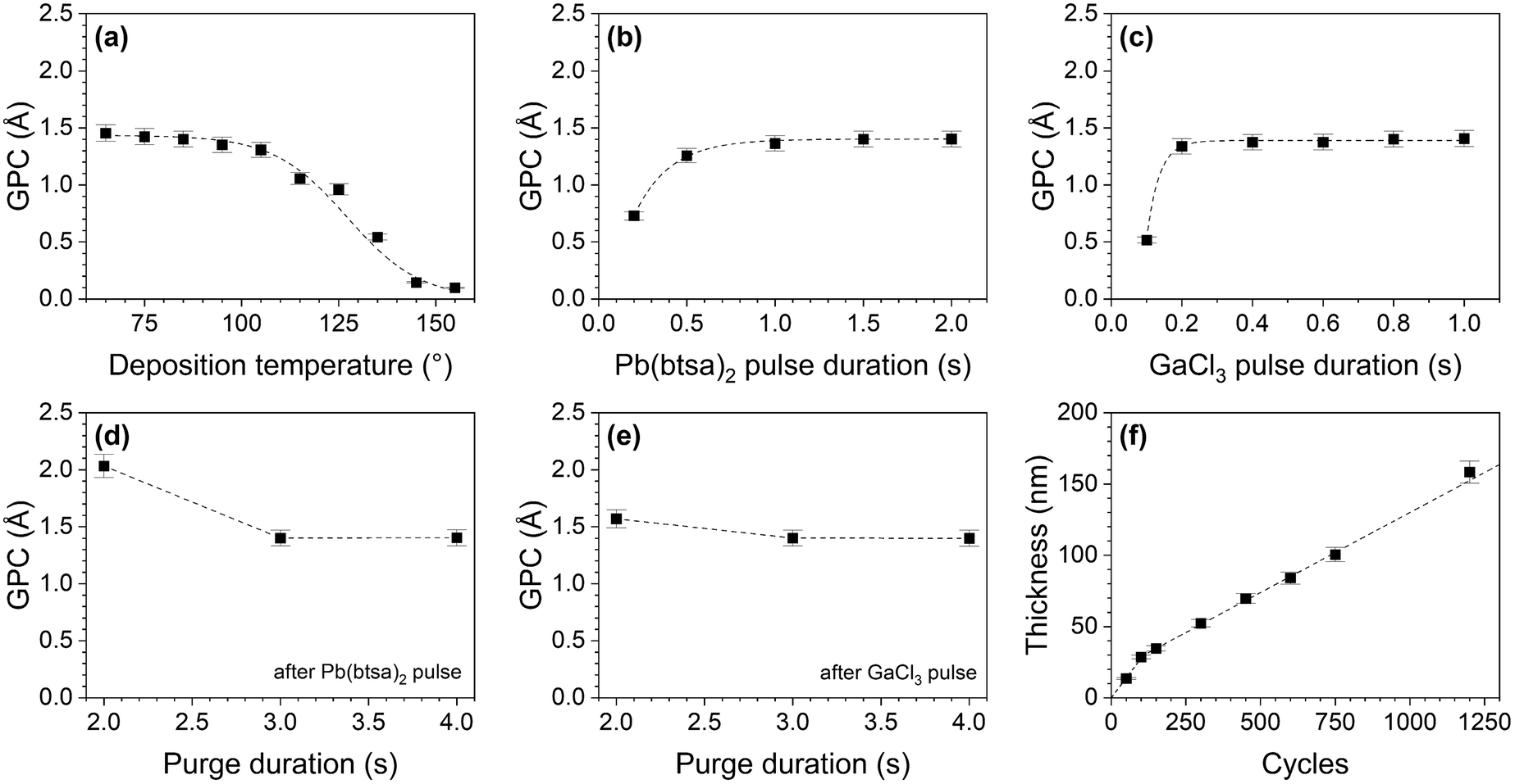 | ||
| Fig. 2 Growth per cycle (GPC) of PbCl2 on silicon as a function of (a) deposition temperature, (b) Pb(btsa)2 pulse duration, (c) GaCl3 pulse duration, (d) purge duration after Pb(btsa)2 pulse and (e) purge duration after GaCl3 pulse. (f) PbCl2 film thickness as a function of deposition cycles. Unless otherwise evident the depositions were made at 85 °C, with 600 cycles of 1.5 s Pb(btsa)2 pulse, 0.8 s GaCl3 pulse and 3.0 s purge durations. Thicknesses were measured with ellipsometry. | ||
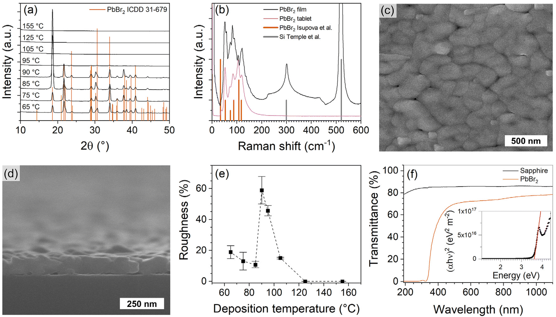
The films are crystalline PbCl2 at all deposition temperatures (Fig. 3a and Fig. S7†). No impurity phases were observed in XRD patterns and Raman spectra of the films (Fig. 3b). Composition analysis with ToF-ERDA shows that the films contain only 1.0 at% gallium as well as some oxygen, hydrogen and traces of nitrogen and carbon (Fig. S8†). The oxygen is concentrated at the film surface and is likely present due to the exposure of the samples to ambient air. This is underpinned by a pungent smell in the containers used for storing PbCl2 films for prolonged times and the observation of opaqueness and minor discoloration of a PbCl2 film after it was stored in ambient conditions (Fig. S9a†). EDS of the air-stored sample showed increased oxygen content, whereas XRD only showed a slight decrease in the intensity of the PbCl2 reflections and no impurity phases (Fig. S9b and c†). Therefore, inert storage conditions are needed to prevent degradation of the PbCl2 films.
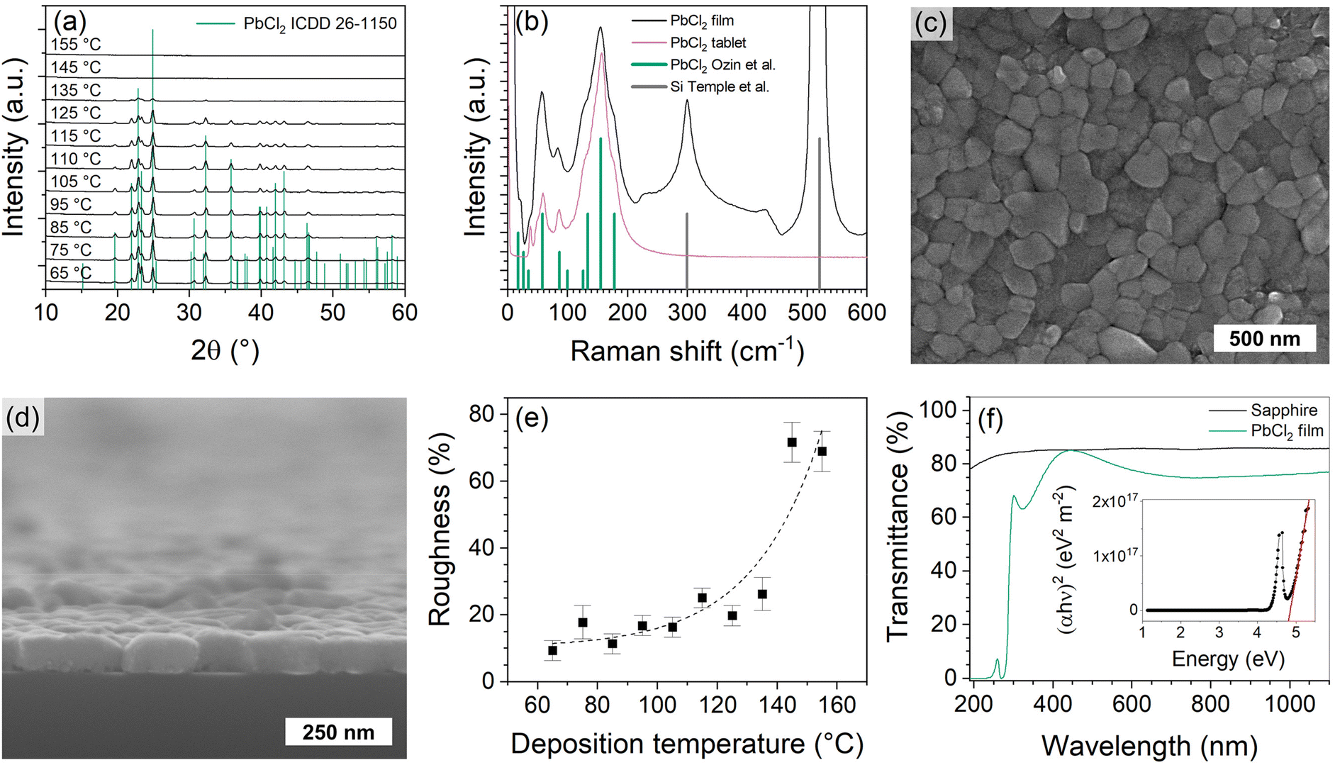 | ||
| Fig. 3 (a) XRD patterns of PbCl2 films deposited at different temperatures. Enlarged and indexed XRD patterns are shown in Fig. S7.† (b) Raman spectra of a PbCl2 film on a thermal SiO2/Si substrate and of a tablet pressed from commercial PbCl2 powder (99.999%, Alfa Aesar). The PbCl2 film was deposited with 1200 cycles. Literature patterns for PbCl278 and Si79 are shown for reference. FESEM image of a PbCl2 film taken (c) top-down and (d) from cross-section. (e) PbCl2 film roughness relative to the thickness as a function of deposition temperature. (f) Transmittance of a PbCl2 film deposited on sapphire and of a bare sapphire wafer as reference. Inset shows the Tauc plot constructed from the transmittance spectrum of the PbCl2 film in (f). The extra features in the transmittance spectrum and the peak in the Tauc plot at 4.5 eV are caused by interference in the film. See Fig. S12† for more details. Unless otherwise evident the depositions were made at 85 °C, with 600 cycles of 1.5 s Pb(btsa)2 pulse, 0.8 s GaCl3 pulse and 3.0 s purge durations. | ||
X-ray photoelectron spectroscopy (XPS) spectra show the same elements as ToF-ERDA (Fig. S10a†) with Pb and Cl being the main constituents. The Pb 4f spectrum consists of two doublets (Fig. S10b†). The higher intensity doublet at 139.2 and 144 eV corresponds to PbCl231 and the lower intensity one at 136.9 eV and 141.7 eV to metallic Pb0.32 Literature is scarce on degradation and XPS studies of binary lead compounds but in the studies on lead halide perovskites, Pb0 was commonly observed and associated with Pb0 defect clusters induced by degradation of the compound in ambient air.33–37 Cl 2p spectrum consists of a single doublet corresponding to PbCl2 (Fig. S10c†).38 Ga 2p spectrum also consists of a single doublet corresponding to Ga2O3 (Fig. S10d†).39,40 GaCl3 is hygroscopic and in ambient air reacts with H2O to form Ga2O3 and HCl.41 Gallium containing by-products formed in the ALD processes are expected to react similarly. Therefore, Ga2O3 most likely originates from either GaCl3 or by-products incorporated into the film during the deposition that subsequently reacted with moisture upon exposure to ambient air. The O 1s spectrum consists of four peaks dominated by contaminants accumulated on the film surface from ambient air (Fig. S10e†). These peaks can be tentatively assigned as follows: at 531.2 eV to Ga2O3 and organic carbon contaminants, 532.2 eV to OH groups, 533 eV to organic carbon contaminants and 534.1 eV to H2O.39,42
PbCl2 films consist of columnar grains (Fig. 3c and d). With the same number of deposition cycles, the size of the grains decreases with increasing deposition temperature (Fig. S11†). An 85 nm thick PbCl2 film deposited at 85 °C had a surface roughness (Rq) of 10 nm, which is 12% of the film thickness. Such roughness is typical for crystalline metal halide films deposited with ALD.10,11 As the deposition temperature increases the relative roughness starts to increase exponentially, because the GPC decreases, causing films deposited with the same number of cycles to become thinner and discontinuous (Fig. 3e).
The optical properties of the PbCl2 films are in good agreement with the literature. The films are transparent in the visible range and absorb in the UV range (Fig. 3f and Fig. S12†). The optical band-gap, extracted from the Tauc plot (Fig. 3f, inset), is 4.9 eV (lit. 4.7–4.9 eV)43–46 and the refractive index of the films was 2.2 (lit. 2.3).16
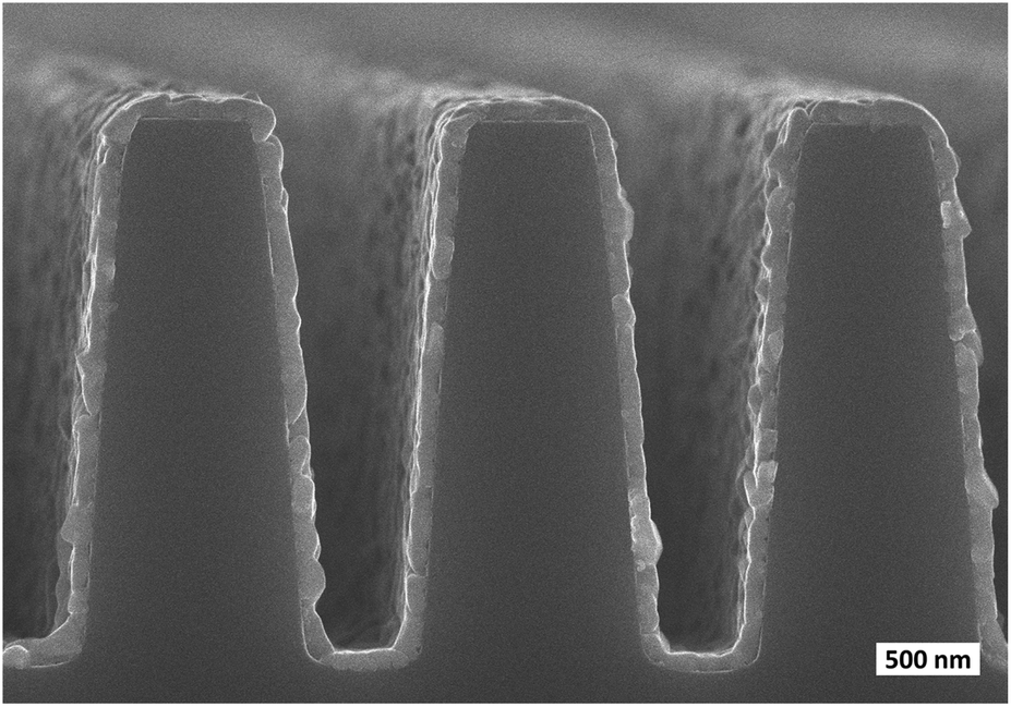
PbCl2 film grew conformally on a patterned Si substrate without any additional optimization of the process parameters (Fig. 4). The film was smooth and consisted of columnar grains similar to the ones observed on the planar Si substrate (Fig. 3c and d).
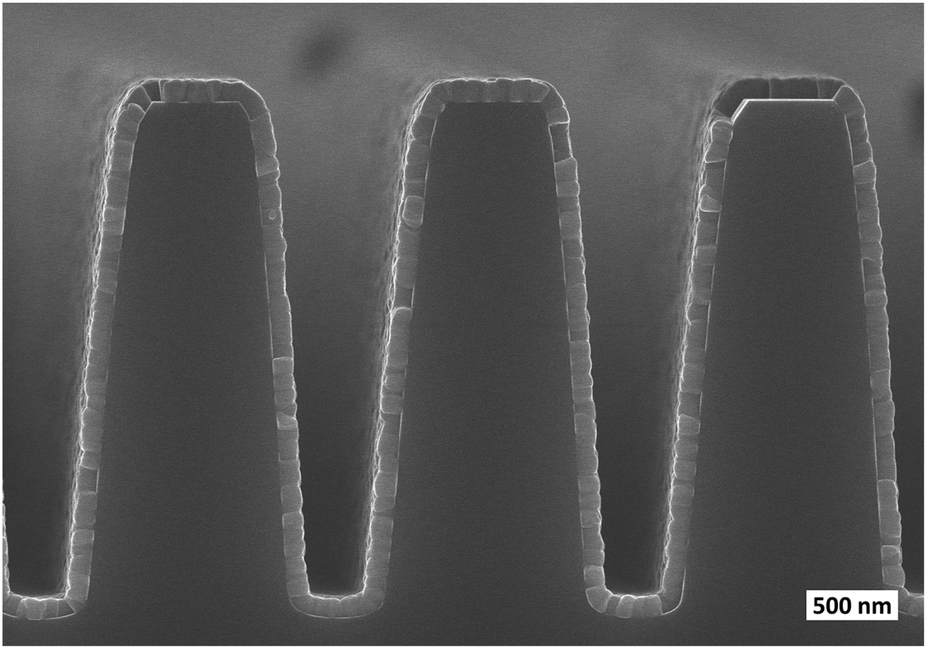 | ||
| Fig. 4 FESEM image of a PbCl2 film deposited on a patterned Si substrate. The trench aspect ratio is 1:2:5 (bottom width to top width to depth). PbCl2 film was deposited at 85 °C with 600 cycles of 1.5 s Pb(btsa)2 pulse, 0.8 s GaCl3 pulse and 3.0 s purge durations. | ||
2.5 Pb(btsa)2–SnBr4 process
Just like for GaCl3, there were initial challenges in the SnBr4 delivery. When delivered from an open glass boat held at room temperature, SnBr4 sublimed completely during the reactor heating stage prior to the deposition experiment. On the other hand, SnBr4 was insufficiently volatile to be delivered from an external precursor container under its own vapour pressure. For these reasons we resorted to the orifice boats developed for GaCl3. No differences in film properties were observed between films deposited with solid SnBr4 delivered from a boat with a 7 × 5 mm orifice and films deposited with an 80 wt% SnBr4 solution in hexane delivered from a boat with a 1 mm orifice. Based on the lack of differences we chose 7 × 5 mm orifice boats for SnBr4 delivery as their loading was more convenient.With 0.07 Å per cycle, the Pb(btsa)2–SnBr4 process had the lowest GPC among the processes presented in this work. This GPC decreased further with increasing deposition temperature (Fig. S13c†). At 65 °C the GPC saturated with respect to the SnBr4 pulse duration and was independent of the purge duration but did not saturate with respect to the Pb(btsa)2 pulse duration (Fig. S13d–f†). The film thickness increased linearly with the number of deposition cycles (Fig. S13g†) and the films had a visible thickness gradient (Fig. S13a†).
The films were amorphous at all deposition temperatures with two very wide features (FWHM 8.4° of 2θ) visible in the XRD patterns (Fig. S13i†). FESEM revealed that the films are smooth and lack any features, as expected from amorphous films (Fig. S13b†). The measured refractive index of 1.9 was lower than the literature values (2.4–2.6)16 reported for PbBr2. Furthermore, the films contained impurities that were mainly Sn, O and H (Fig. S13h†). The Pb to Br ratio, on the other hand, was close to stoichiometric and the observed element concentrations were similar to those in the (Pb(gem))2–SnCl4 process. Following the same reasoning, we speculate that the addressed impurity contents are caused by an incorporation of an air sensitive by-product during the deposition.
To explain the differences between the Pb(btsa)2–SnX4 deposition behaviour (Table 1) we performed a quantum chemical investigation using ORCA 5 and the general-purpose composite density functional theory (DFT) method r2SCAN-3c47 (Table 2). In general, reactions that produce crystalline PbX2(s) were highly favourable (ΔG ≤ −110 kJ mol−1), including disproportionation of the heteroleptic Pb(btsa)X(g) to Pb(btsa)2(g) and PbX2(s), which supports our observations here and previously10 that SnX4 can deposit crystalline PbX2.
| Reaction | Type | X = Cl | Br | I |
|---|---|---|---|---|
| Pb(btsa)2 + SnX4 → PbX2(s) + Sn(btsa)2X2 | Deposition | −228 | −213 | −192 |
| Pb(btsa)2 + Sn(btsa)X3 → PbX2(s) + Sn(btsa)3X | Deposition | −137 | −124 | −110 |
| Pb(btsa)2 + SnX4 → Pb(btsa)X + Sn(btsa)X3 | Intermediate | −68 | −63 | −50 |
| Pb(btsa)2 + PbX2(s) → 2Pb(btsa)X | Intermediate | 107 | 95 | 91 |
| 3Pb(btsa)2 + SnX4 → 3Pb(btsa)X + Sn(btsa)3X | Intermediate | −97 | −92 | −69 |
| Pb(btsa)X + Sn(btsa)3X → Pb(btsa)2 + Sn(btsa)2X2 | Etch | −24 | −26 | −33 |
We then investigated by quantum chemical calculations the reaction that causes etching with SnCl4, but deposition with SnBr4 and SnI4. We speculated that Pb(btsa)2 itself was the only etch product capable of removing Pb(II) ions from the film at such low temperatures, and found that the only favourable reaction resulting in Pb(btsa)2 formation is between Pb(btsa)X(g) and Sn(btsa)3X(g). The free energy change of this reaction is, contrary to the experimental evidence, larger for the iodide than the bromide or chloride, but the difference was too small (ΔG ∼ 4 kJ mol−1) to be considered definitive evidence at the chosen level of theory. Besides, the free energy change of the reactions for each halide was small (−33 < ΔG < −24 kJ mol−1). However, the formation of the reactive intermediates Sn(btsa)3X(g) and Pb(btsa)X(g) from 3 eq. of Pb(btsa)2(g) and 1 eq. of SnX4(g) was most favourable for the chloride (ΔG = −97 kJ mol−1), followed closely by the bromide (ΔG = −92 kJ mol−1), while it was far less favourable for the iodide (ΔG = −69 kJ mol−1). As the reason for the etching observed when using SnCl4 and the impurities observed when using SnBr4, we propose a higher volatility of the intermediate heteroleptic Sn(IV) amide chlorides than the analogous bromides. This common trend between analogous group 17 compounds would cause the chlorides to evaporate (i.e., cause etching) while the bromides would not (i.e., incorporate air-sensitive impurities). On the other hand, it seems far less favourable for the heteroleptic intermediates to form for the iodide, which results in ALD of pure PbI2 films from Pb(btsa)2 and SnI4.10
2.6 Pb(btsa)2–TiBr4 process
The Pb(btsa)2–TiBr4 process deposits uniform PbBr2 films (Fig. 5a and b inset). The GPC is independent of the deposition temperature in the 65–85 °C range and decreases abruptly when the deposition temperature increases above 85 °C (Fig. 5b). At 75 °C the GPC is independent of the purge durations when they are 0.5 s and longer (Fig. 5c) and saturates with respect to both precursor pulse durations (Fig. 5d and e). The film thickness at 75 °C increases linearly with an increasing number of cycles, apart from an initial steeper slope, that we attribute to enhanced nucleation on Si (Fig. 5f).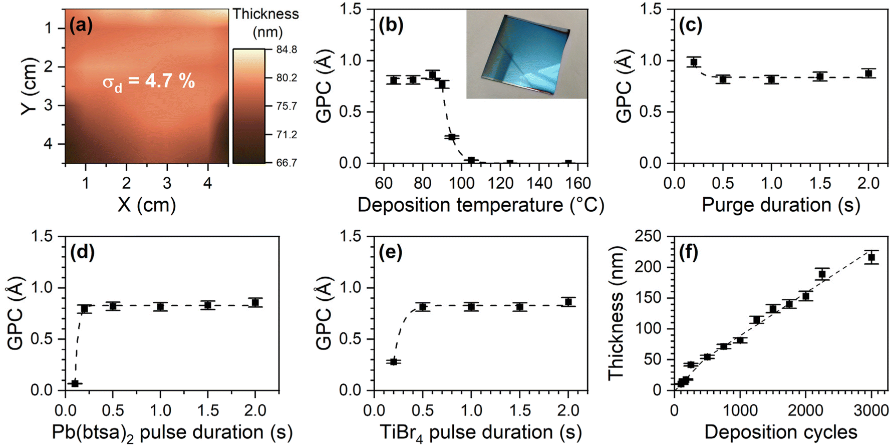 | ||
| Fig. 5 (a) Ellipsometry thickness maps of a PbBr2 film deposited on 5 × 5 cm Si substrate (0.5 cm edge exclusion). PbBr2 GPC as a function of (b) deposition temperature as well as (c) purge, (d) Pb(btsa)2 pulse and (e) TiBr4 pulse duration. (f) Shows PbBr2 film thickness as a function of deposition cycles. The inset in (b) is a digital photograph of a PbBr2 film. In (c) both purge durations were adjusted in a single deposition experiment. Unless otherwise evident the films were deposited at 75 °C with 1000 cycles. The pulse durations were 1.0 s and 1.5 s long for Pb(btsa)2 and TiBr4 respectively and were separated by 1.0 s long purges. Thicknesses were measured by ellipsometry. | ||
XRD and Raman show that the films deposited with the Pb(btsa)2–TiBr4 process were crystalline PbBr2 (Fig. 6a and b). Grain boundaries in the PbBr2 films are not as evident as in the PbCl2 films made with GaCl3 (Fig. 6c, d and Fig. S15†). Upon growth, PbBr2 grains partially coalesce together into clusters that give the films their botryoidal texture. A higher deposition temperature promotes the fusion of grains, causing the films to become smoother (Fig. 6e). At 90 °C the GPC decreases abruptly (Fig. 5b), the films deposited with the same number of cycles become thinner and discontinuous which causes an increase in relative roughness. No deposition occurs at temperatures higher than 105 °C (Fig. 5b and Fig. S15f–h†). An 81 nm thick film deposited at 75 °C, had an 11 nm surface roughness (Rq) which is 13% of the film thickness and is in the range of what we typically observe for crystalline halide films made via ALD.10,11
 | ||
| Fig. 6 (a) XRD patterns of PbBr2 films deposited at different temperatures. Enlarged and indexed XRD patterns are shown in Fig. S14.† (b) Raman spectra of PbBr2 film on thermal SiO2/Si substrate and of a tablet pressed from commercial PbBr2 powder (99.998%, Alfa Aesar). The PbBr2 film was deposited with 1600 cycles. Literature patterns for PbBr280 and Si79 are shown for reference. FESEM image of a PbBr2 film taken (c) top-down and (d) from cross-section. (e) PbBr2 film roughness relative to thickness as a function of deposition temperature. (f) Transmittance of a PbBr2 film deposited on sapphire and of a bare sapphire wafer. Reflectance spectrum is shown in Fig. S19.† Inset shows the Tauc plot constructed from the transmittance spectrum of the PbBr2 film in (f). Unless otherwise evident the depositions were made at 75 °C, with 1000 cycles of 1.0 s Pb(btsa)2 pulse, 1.5 s TiBr4 pulse and 1.0 s purge durations. | ||
ToF-ERDA shows that small amounts of titanium (0.5 at%) are present in the films as well as some lighter elements with oxygen having the highest concentration (Fig. S16†). The same elements are also visible in the XPS spectra (Fig. S17a†). Like the Pb 4f spectra of the PbCl2 film, the Pb 4f spectrum of the PbBr2 film consists of two doublets (Fig. S17b†). The higher intensity doublet (139.1 and 144 eV) corresponds to PbBr248 and the lower intensity one (136.9 and 141.8 eV) to Pb0.32 The Br 3d spectrum features a single doublet corresponding to PbBr2.48 Titanium Ti 2p spectrum is also a single doublet that fits TiO2 (Fig. S17d†).49 A component corresponding to the oxygen in the TiO2 is also present in the O 1s spectrum (530.6 eV, Fig. S17e†).49 Otherwise, the O 1s spectrum of the PbBr2 film (Fig. S17e†) is comprised of similar oxygen containing surface contaminants as in the case of PbCl2 (Fig. S10e†).42 Since the deposition process is oxygen free, the oxygen content most likely originates from the exposure of the PbBr2 film to air. In case of PbBr2 films, XRD shows that lead oxybromide hydrate starts to form upon prolonged exposure to air (Fig. S18†).
The optical properties of the PbBr2 films correspond to those reported for PbBr2 in literature. The refractive index is 2.5 (lit. 2.4–2.6)16 and the band gap extracted from the Tauc plot, that was constructed from the transmittance data (Fig. 6g), is 3.7 eV (lit. 3.8–4.2 eV43–46,50). A comparison of film compositions and refractive indices across the studied processes (Table 1) suggests that a significant impurity content causes a significant deviation of the observed refractive index from that of the bulk compound. Mind, that a small decrease in the refractive index relative to the bulk value is common for thin film samples.51,52
Just like PbCl2 deposited with GaCl3, PbBr2 deposited with TiBr4 grew conformally on a patterned Si substrate with no need for any additional optimization of process parameters (Fig. 8). Due to the crystallite texture that the PbBr2 process yields, the PbBr2 film is rougher than the PbCl2 film (Fig. 4).
We constructed simple UV photodetectors (photoresistors, Fig. 7a–c) to test whether Pb(btsa)2–GaCl3 and Pb(btsa)2–TiBr4 processes deposit films of sufficient quality for optoelectronic devices. As expected for the wide band-gap materials, the dark current was small (10−11 A) and under UV illumination the current increased several orders of magnitude (Fig. 7d). The PbCl2 based photodetector exhibited a larger increase in current under the UV illumination compared to the PbBr2 based device. These simple devices show that the halide films can be used in optoelectronic devices.
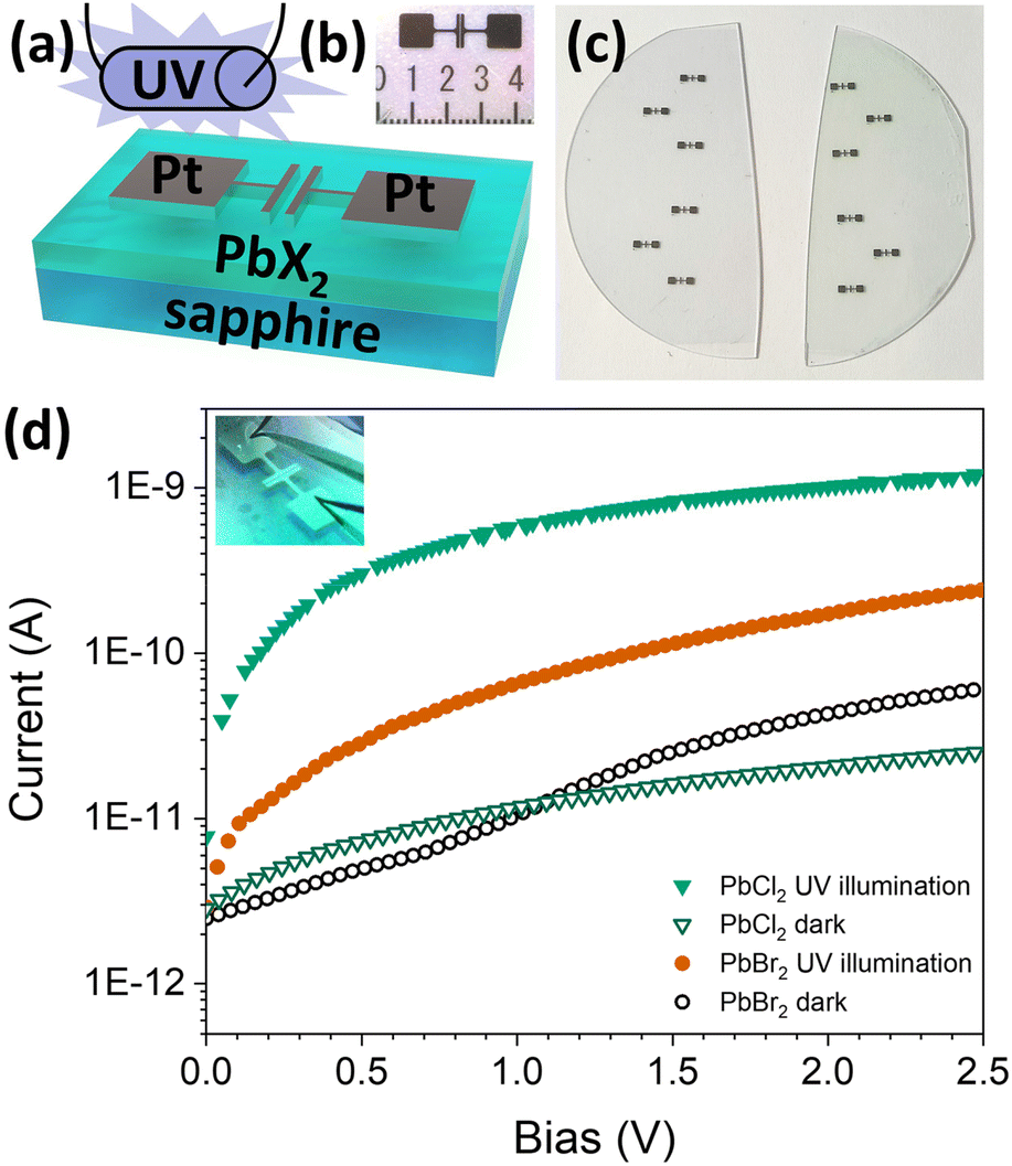 | ||
| Fig. 7 (a) Schematic structure and (b) photograph of the sapphire/lead halide/Pt photodetector structure. Millimetre ruler is shown for reference. (c) Photograph of the PbCl2 based (left) and PbBr2 based (right) device structures. (d) I–V curves of a PbCl2 and PbBr2 devices from (c) in dark and under UV illumination. Inset photograph shows a PbBr2 based device with needle probe contacts under UV illumination. The PbCl2 film was deposited at 85 °C with 600 cycles consisting of 1.5 s Pb(btsa)2 pulse, 0.8 s GaCl3 pulse and 3.0 s purge durations. The PbBr2 film was deposited at 75 °C with 2900 cycles consisting of 1.0 s Pb(btsa)2 pulse, 1.5 s TiBr4 pulse and 1.0 s purge durations. | ||
 | ||
| Fig. 8 FESEM image of a PbBr2 film deposited on a patterned Si substrate. The trench aspect ratio is 1:2:5 (bottom width to top width to depth). PbBr2 film was deposited at 75 °C with 1000 cycles of 1.0 s Pb(btsa)2 pulse, 1.5 s TiBr4 pulse and 1.0 s purge durations. | ||
2.7 Mixed lead halides
PbCl2 and PbBr2 are isostructural with the cotunnite structure (Fig. S20a and b†)53 whereas PbI2 has a 2D structure with a large number of polytypes that differ from each other in how the 2D layers stack on top of each other (Fig. S20c and d†).54 Each pair of the binary lead halide compounds can form a ternary compound: PbBrCl, PbICl and PbBrI. Also, the ternary compounds adopt the cotunnite structure (Fig. S20e–g†).We used the supercycle approach to test whether the binary halide processes are compatible with each other and whether mixed lead halides can be deposited. The processes that we chose were Pb(btsa)2–GaCl3 for PbCl2, Pb(btsa)2–TiBr4 for PbBr2 and Pb(btsa)2–SnI4 for PbI2.10 The deposition experiments consisted of 50 supercycles which in turn consisted of 20 binary process cycles of two lead halides yielding a total of 1000 deposition cycles (Fig. 9). We varied the ratio between the binary lead halide process cycles and studied how that affected the element concentrations, phase composition and optical properties of the films.
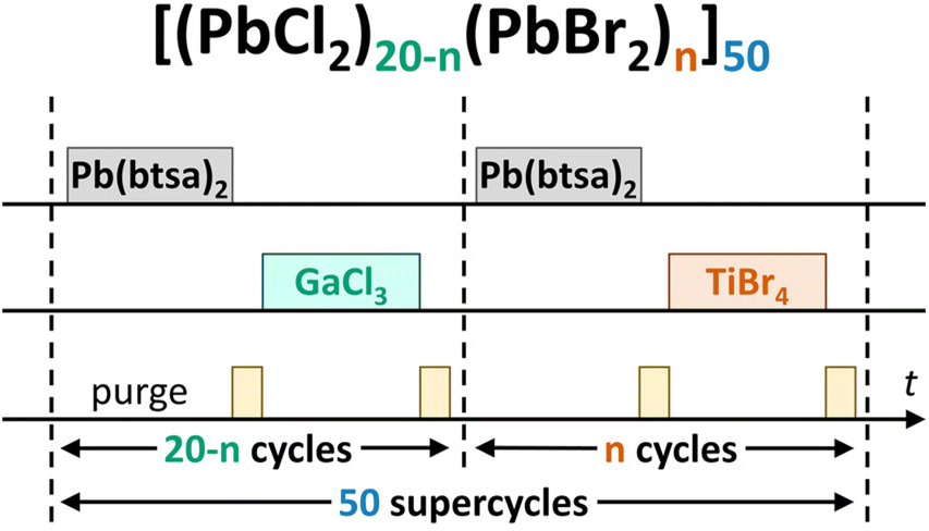 | ||
| Fig. 9 Scheme of a pulse sequence used to deposit mixed lead halides. PbCl2 and PbBr2 binary processes are used as an example. The total number of deposition cycles was always 1000, as n ≤ 20. | ||
Composition of the mixed lead halide films does not have a linear dependence on the ratio of the binary lead halide processes. This lack of the linear dependence is common for the supercycle approach.55–58 In the PbCl2–PbBr2 and PbBr2–PbI2 systems, the composition is shifted heavily in favour of the heavier halide (Fig. 10a and g). Only a couple of cycles of the heavier halide in the supercycle cause a significant composition deviation. The effect is stronger in the PbCl2–PbBr2 system. On the other hand, in the PbCl2–PbI2 system the deviation in the halide content from the ratio of the binary process cycles is more gradual with a plateau at around 1:1 halide ratio for the intermediate cycle ratios (Fig. 10d). In the supercycle approach a difference in GPCs of the binary processes can cause nonlinear dependence of the composition on the ratio of binary process cycles. In our case, however, the GPC trend is reverse with PbCl2 having the highest GPC and PbI2 the lowest. Another possible explanation is that in mixed halide processes a halide exchange reaction occurs, followed by distribution of the heavier halide in the film via diffusion.
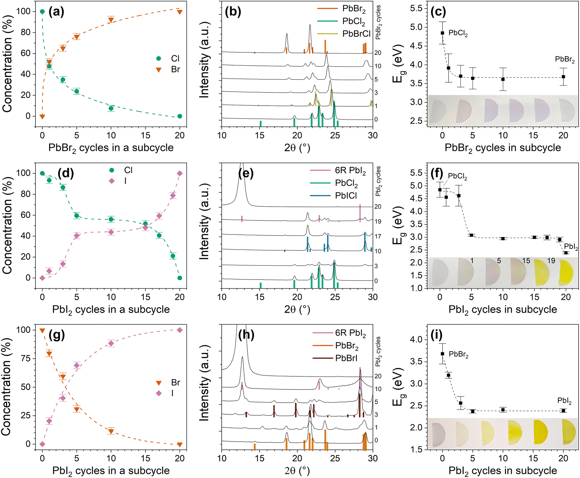 | ||
| Fig. 10 (a) Halide concentration, (b) XRD patterns and (c) bandgaps of PbBrxCl2−x films. (d–f) and (g–i) Show same sets of data for PbIxCl2−x and PbBrxI2−x respectively. Insets show digital photographs of mixed halide films deposited on sapphire that were used for transmittance measurements. Bandgaps were extracted from Tauc plots constructed from this transmittance data. Halide concentrations are obtained from EDS measurements and normalized to the total halide content. Relevant XRD reference patterns, including PbBr2 (ICDD 31-679), PbCl2 (ICDD 26-1150), PbBrCl (ICDD 24-1088), 6R PbI2 (COD 9009142), PbICl (ICDD 43-949) and PbBrI (ICSD 22138) are shown. All films were deposited at 75 °C. XRD patterns in a wider 2θ range are shown in Fig. S21.† | ||
The PbCl2–PbBr2 system is a solid solution. At all the examined cycle ratios, the films are phase pure PbBrxCl2−x (Fig. 10b and Fig. S21a†). Mixed halide cotunnites also form in the PbCl2–PbI2 and PbBr2–PbI2 systems but minor reflections of one or both binary phases are always present in the XRD patterns of the films (Fig. 10e, h and Fig. S21b, c†). The films look homogenous when examined with SEM (Fig. S22†). This, however, does not contradict the presence of the binary phases as they can segregate at the grain boundaries instead of forming separate macro-scaled domains.
In all the systems changes in the optical properties of the films follow changes in the composition of the films (Fig. 10c, f and i). The bandgap of the films can be tuned in a range from 2.4 to 4.9 eV.
The Pb(btsa)2–GaCl3, –TiBr4 and –SnI4 processes are compatible with each other. We saw no signs of undesirable side reactions or phases. However, there is room for further optimization of the supercycle's parameters. Given the non-linear dependence of the composition on the cycle ratios in all the three systems, an increase in the total number of binary process cycles that comprise the supercycle will enable finer composition tunability on the lighter halide end.
3. Conclusions
We showed that PbCl2 and PbBr2 can be deposited with ALD at low temperatures (≤100 °C). The Pb(btsa)2–GaCl3 and the Pb(btsa)2–TiBr4 processes produce the films with the best properties. These processes deposit pure, crystalline, uniform and conformal films. All other processes that we studied namely Pb(btsa)2–SnCl4, Pb(btsa)2–SnBr4, Pb(btsa)2–TiCl4 and (Pb(gem))2–SnCl4 were found to be unideal as ALD processes. The observed issues showcase how subtle differences in the halide precursors have major impact on the behaviour of by-products and ultimately on the film properties. This, in turn, highlights the importance of empirical and computational mechanism studies for further development of metal halide ALD processes.Furthermore, we showed that mixed lead halide films can be deposited with ALD. Pb(btsa)2–GaCl3 and –TiBr4 processes are compatible with each other as well as with the earlier reported Pb(btsa)2–SnI4 process for PbI2. One plausible direction for future research efforts is further optimization of the mixed lead halide process parameters and their conversion to halide perovskites.
4. Experimental
4.1 Precursors
Pb(btsa)2 was synthesized from PbCl2 (99.999%, Alfa Aesar) and Li(btsa) (97%, Sigma Aldrich) using Schlenk line techniques. The synthesis procedure is based on the work of Gynane et al.59 Li(btsa) dissolved in n-hexane was added dropwise to PbCl2 in THF over a cold water bath. The bottle was wrapped in an aluminium foil to protect the mixture from light and left to stir overnight. THF was removed in vacuo and replaced with n-hexane. The mixture was filtered through a glass filter frit with Celite yielding a clear canary yellow solution. Removal of hexane in vacuo affords a red orange Pb(btsa)2 oily liquid. The liquid can be used as is, but it slowly decomposes during storage inside glove box despite protection from light. Decomposition is visible by the darkening colour of the liquid with time. Pb(btsa)2 is reported to be solid at room temperature.23,59 Distillation of the liquid Pb(btsa)2 still yielded a liquid. Cooling the distillate with liquid N2 caused it to solidify into a bright yellow solid. The solid does not melt upon warming back to room temperature and is stable upon storage. Solid 1H NMR (400.144 MHz, 298 K, C6D6): δ 0.25 (s, 36 H). 13C NMR (100.616 MHz, 298 K, C6D6): δ 5.93. In film depositions there were no differences regardless of whether liquid or solid Pb(btsa)2 was used. Literature provides more data on the sensitivity and stability of Pb(btsa)2.21,23,59Bis[lead(II) N,N′-di-tert-butyl-1,1-dimethylsilanediamide] (Pb(gem))2 was prepared following a literature procedure.60 Dilithio diamide Me2Si[N(Li)tBu]2 (1 eq., 7.928 g, 37.00 mmol), recrystallized from hexane, and a slight excess of PbCl2 (1.1 eq., 11.31 g, 40.70 mmol) were placed in a 250 mL round-bottom flask with a magnetic stir-bar in a N2-filled dry-box. Then, 100 mL of Et2O was added all at once and the flask was closed with a greased glass stopper held shut with a plastic Keck clip. A slight exotherm occurs as the dilithio salt dissolves and begins to react with PbCl2. The reaction mixture was then stirred overnight (ca. 16 h). After the reaction had proceeded, an off-white precipitate developed under a bright orange supernatant liquid which was separated by filtration through a pad of Celite and a medium porosity sintered glass filter to yield a bright orange filtrate. (Note: If crude or in situ generated Me2Si[N(Li)tBu]2 is used, a dark precipitate, presumably contaminated with Pb(0), may be obtained with a slightly diminished yield.) Solvent and other volatiles were removed under vacuum, and a crude orange solid was obtained. The crude product was then purified directly by vacuum sublimation (100 °C/40 mTorr) into an air-cooled 90° glass elbow to yield (Pb(gem))2 as yellow thermochromic crystals that turn orange upon heating and red upon melting (14.04 g, 92% yield based on ligand). M.p. 85 °C, sublimed; lit. 85 °C, recrys. Et2O. Crystals suitable for X-ray diffraction were grown by slowly cooling a solution of (Pb(gem))2 in toluene overnight at −49 °C. 1H NMR (300 MHz, C6D6, δC6D5H = 7.16 ppm): 0.42 (6H, s, Si(CH3)2), 1.24 (18H, s, PbN–C(CH3)3). More data on the sensitivity and stability of (Pb(gem))2 can be found in literature.21
Crystals were attached to the tip of an appropriately sized MiTeGen mount with Paratone-N oil. Measurements were made on a Bruker APEXII CCD equipped diffractometer using monochromated Mo Kα radiation (λ = 0.71073 Å; 30 mA, 50 mV) at 125 K. APEX3 software61 was used for the initial orientation and unit cell were indexed using a least-squares analysis of a random set of reflections collected from three series of 0.5° wide scans, 10 seconds per frame and 12 frames per series that were well distributed in reciprocal space. For data collection, four ω-scan frame series were collected with 0.5° wide scans, 5 seconds frames and 366 frames per series at varying φ angles (φ = 0°, 90°, 180°, 270°). The crystal to detector distance was set to 6 cm and a complete sphere of data was collected. Cell refinement and data reduction were performed with the Bruker APEX3 software, which corrects for beam inhomogeneity, possible crystal decay, Lorentz and polarization effects. Data processing and a multi-scan absorption correction was applied using APEX3 software package. The structure was solved using the SHELXT62 using Intrinsic phasing and all non-hydrogen atoms were refined anisotropically with the SHELXL63 using a combination of the ShelXle graphical user interface64 and OLEX2.65
Commercial halides: SnCl4 (98%, STREM), SnBr4 (99%, Sigma Aldrich), SnI4 (99+%, 10 mesh, Thermo Scientific Acros) and TiCl4 (99.9%, Sigma Aldrich) were used as received. TiBr4 (98%, Sigma Aldrich) was ground from as received cm sized chunks to mm sized grains. GaCl3 (ABCR, 99.999%) was dissolved in n-hexane (25 wt%). SnI4, SnBr4, TiBr4 and GaCl3 were stored and handled in glove box. Note that TiBr4 and GaCl3 readily evaporate out of their containers once opened and TiBr4 vapour stains solid objects in contact with it. We recommend storing an opened container inside a second larger container, as neither wax film nor electrical tape can entirely prevent this issue.
4.2 Film deposition
Deposition experiments were performed using a commercial, hot-wall, flow type F120 ALD reactor (ASM Microchemistry Ltd). The pressure in the deposition chamber was ca. 10 mbar. Nitrogen (AGA, 99.999%) at a flow rate of 400 sccm was introduced into the reactor through a gas purifier (SAES Pure Gas, MC1-902F, H2O, O2, CO, CO2, H2, NMHC removal <1 ppb) and acted as carrier and purge gas. SnCl4 and TiCl4 were delivered from external containers where they were held at room temperature. Their delivery lines were equipped with bellows-sealed metering valves (Cv 0.019, Swagelok) that were used to control the dose of the precursor pulsed with solenoid valves. The metering valve was opened for ½ turn for SnCl4 and TiCl4. Pb(btsa)2, SnI4 and TiBr4 were sublimed from open glass boats held at 60, 65 and 25 °C respectively and pulsed with inert gas valving. SnBr4 was sublimed from closed glass boats with 7 × 5 mm orifice at 25 °C. GaCl3 solution in hexane was sublimed from closed glass boats with a 1 mm orifice at 25 °C. When the reactor is evacuated, hexane evaporates leaving the solid GaCl3 inside closed glass boats (Video S1†).Most of the depositions were done on 5 × 5 cm native oxide covered silicon substrates (Okmetic). 6′′ Si wafers were cut into 5 × 5 cm square pieces which were sonicated thrice: first at 50 °C for 20 min in deionized water (DI) with 20 ml detergent (Branson Industrial Strength Cleaner Concentrate), next at RT for 10 min in DI and finally at RT for 10 min in isopropanol. Clean Si was dried in a heating cabinet at 100 °C for 20 min and prior to loading into the ALD reactor, blown with N2 to remove dust. Si substrates with thermal SiO2 were prepared similarly. Some depositions were made on sapphire wafers (2′′, University Wafer). Prior to usage the sapphire wafers were heated at 1000 °C in an air oven for 2 h to induce atomic step formation.66,67
Most of the deposited films were stored in a desiccator. Films used for composition analysis were stored in a glove box. However, sample preparation and transfer between storage locations took place in ambient air.
4.3 Film characterization
Film thicknesses were measured either with ellipsometry or with energy dispersive X-ray spectroscopy (EDS). Ellipsometry measurements were made with a Film Sense FS-1 multi-wavelength ellipsometer. Ellipsometry data was fitted with the Cauchy model, which also modelled refractive index values. The reported refractive indices are those for a wavelength of 580 nm. The errors in ellipsometry thickness values were estimated from the fit difference values. EDS was used instead of ellipsometry for processes where the ellipsometry data fit was poor due to roughness, ambiguous composition, or a thickness gradient.EDS measurements were performed with an Oxford INCA 350 energy spectrometer connected to a Hitachi S-4800 field emission scanning electron microscope (FESEM). Thicknesses were calculated from the EDS data (k ratios) using the GMRFilm software68 and bulk densities (5.85 and 6.66 g cm−3 for PbCl2 and PbBr2 respectively). The errors in EDS thickness values were estimated from weight% uncertainty values of EDS data.
A Hitachi S-4800 field emission scanning electron microscope (FESEM) and a Veeco Multimode V instrument (atomic force microscopy, AFM) were used to study film morphology. AFM tapping mode images were captured in air using two types of silicon probes: NFESP (discontinued) and RFESP-75, both from Bruker. Both probes had a spring constant of 3 N m−1 and nominal tip radius of 10 nm. AFM images were flattened to remove artefacts caused by sample tilt and scanner bow. Roughness was calculated as a root-mean-square value (Rq) from flattened images.
X-ray diffraction (XRD) patterns were measured in grazing incidence (GI) geometry with an incident angle of 1°. Most measurements were made on a Rigaku Smartlab diffractometer with Cu Kα-radiation. The measurements regarding the Pb(btsa)2–SnBr4 process and stability tests as well as those of the mixed lead halide films were made with a PANalytical X'pert Pro MPD diffractometer also with Cu Kα-radiation.
The samples used for Raman measurements were deposited on Si wafers with a 320 nm layer of thermal SiO2. The thickness of the measured film was optimized to achieve amplification in the Raman signal through the interference effect.69,70 To measure the micro-Raman spectra in a backscattering geometry, a confocal Raman microscope (NT-MDT Ntegra), equipped with a 633 nm laser and a 100× objective, was used. The incident power was 4.5 mW and the spectra were measured with 10 exposures that were 9 s long for PbCl2 and 20 s long for PbBr2.
The elemental compositions of the films were assessed with time-of-flight elastic recoil detection analysis (ToF-ERDA) using a 5 MV tandem accelerator at the accelerator laboratory of the University of Helsinki. The measurements were made with a 40 MeV 127I8+ beam. The incident beam angle and the detector angle relative to the sample surface was 20°.
Transmittance and reflectance in a wavelength range of 190–1100 nm was measured with a Hitachi U2000 spectrophotometer. An evaporated aluminium mirror served as a reference for the reflectance measurements. Optical band gap values were extracted from Tauc plots constructed from the transmittance data. The band gaps of PbCl2 and PbBr2 were assumed to be direct and allowed.
The XPS measurements were made with a Prevac system featuring an EA-15 hemispherical electrostatic energy analyser and RMC50 monochromatic X-ray source with an Al Kα anode (1486.7 eV). The measurements were conducted under ultrahigh vacuum (10−10 mbar) and without sputtering. The survey spectra were taken with 200 eV pass energy and slit S 2.5 × 25. The individual spectra were measured with 100 eV pass energy and slit C 0.8 × 25. Metallic lead (99.999%, BDH) was measured and as the reference point the position of the Pb 4f7/2 in metal state (136.9 eV) was used for these data. Casa XPS software was used to analyse the XPS data. The Tougaard background and LA line shape were used to fit the spectra.
4.4 Photodetector structures
Photodetector structures were made by evaporating platinum electrodes (40 nm) through an Ossila E421 source–drain shadow masks (channel length 30 μm and width 1 mm) onto the lead halide films deposited on sapphire wafers. Needle probes were used to contact the Pt contact pads. The electrical measurements were performed using a Keithley 2450 Source Meter. An in-house mercury vapor discharge lamp was used for UV illumination. The lamp emits primarily at 184 nm (6.7 eV) and 254 nm (4.9 eV).4.5 Quantum chemical calculations
All calculations were carried out with ORCA 5.0.271 using default settings (i.e., grid sizes, convergence criteria, etc.). Initial guess geometries were drawn by hand in Avogadro 1.2.0.72 Geometry optimizations and analytic frequency calculations were then performed with the composite density functional theory (DFT) method r2SCAN-3c,47 which combines the r2SCAN meta-generalized gradient approximation (mGGA) exchange–correlation functional,73 refitted charge-dependent D4 London dispersion correction,73–75 geometric counter-poise (gCP) basis set superposition error (BSSE) correction,73,76 and the def2-mTZVPP atomic orbital basis set. Stationary points were confirmed to have all real frequencies, and all thermodynamic quantities were calculated using default settings under standard conditions in the gas phase. For reactions producing crystalline PbX2(s), the known sublimation free energies under standard conditions (HSC Chemistry 5.11, Outokumpu Research Oy) were included to better model the solid–gas surface chemistry. Illustrations of the calculated geometries were rendered procedurally with Jmol77 and may be found in the ESI† along with electronic energies and thermodynamic corrections of relevant molecular species (Tables S1–S3†).
Author contributions
Conceptualization: G. P. Data Curation: G. P. Formal analysis: G. P. and G. B. Funding acquisition: G. P., G. B., M. L., S. T. B., M. R. and M. K. Investigation: G. P., G. B., C. V. D., L. S. J., A. W., M. M., A. V., M. C., P. J., K. M. and J. D. M. Methodology: G. P. and G. B. Project administration: G. P. Resources: G. P., G. B., C. V. D., L. S. J., A. W., M. M., A. V., M. C., P. J., K. M., M. L., J. D. M., S. T. B., M. R. and M. K. Software: G. B. and J. D. M. Supervision: G. P., S. T. B., M. R. and M. K. Validation: G. P. Visualization: G. P., G. B., C. V. D. and L. S. J. Writing – original draft preparation: G. P. Writing – review and editing: G. P., G. B., C. V. D., L. S. J., A. W., M. M., A. V., M. C., M. L., J. D. M., S. T. B., M. R. and M. K.Conflicts of interest
There are no conflicts to declare.Acknowledgements
We thank Dr Marko Vehkamäki for the Pt deposition on a very short notice. We thank the Finnish Center of Excellence in Atomic Layer Deposition (ALDCoE 2012–2017, decision number 284623) and additional support from the Academy of Finland (decision number 330086). ALD center Finland is thanked for providing access to tools and instruments. G. P. acknowledges the doctoral program in Materials Research and Nanosciences (MATRENA) of the University of Helsinki as well as Emil Aaltonen and Walter Ahlström foundations for funding and support. G. B. thanks the Digital Research Alliance of Canada for computer time on the Cedar cluster.References
- W. A. Dunlap-Shohl, Y. Zhou, N. P. Padture and D. B. Mitzi, Synthetic Approaches for Halide Perovskite Thin Films, Chem. Rev., 2019, 119, 3193–3295 CrossRef CAS.
- A. K. Jena, A. Kulkarni and T. Miyasaka, Halide Perovskite Photovoltaics: Background, Status, and Future Prospects, Chem. Rev., 2019, 119, 3036–3103 CrossRef CAS PubMed.
- L. Chouhan, S. Ghimire, C. Subrahmanyam, T. Miyasaka and V. Biju, Synthesis, optoelectronic properties and applications of halide perovskites, Chem. Soc. Rev., 2020, 49, 2869–2885 RSC.
- H. Kim, J. S. Han, J. Choi, S. Y. Kim and H. W. Jang, Halide Perovskites for Applications beyond Photovoltaics, Small Methods, 2018, 2, 1700310 CrossRef.
- B. Jeong, H. Han and C. Park, Micro- and Nanopatterning of Halide Perovskites Where Crystal Engineering for Emerging Photoelectronics Meets Integrated Device Array Technology, Adv. Mater., 2020, 32, 2000597 CrossRef CAS.
- X.-K. Liu, W. Xu, S. Bai, Y. Jin, J. Wang, R. H. Friend and F. Gao, Metal halide perovskites for light-emitting diodes, Nat. Mater., 2021, 20, 10–21 CrossRef CAS PubMed.
- Y. Zhou, J. Chen, O. M. Bakr and O. F. Mohammed, Metal Halide Perovskites for X-ray Imaging Scintillators and Detectors, ACS Energy Lett., 2021, 6, 739–768 CrossRef CAS.
- F. Li, W. Yu, X. Guan and T. Wu, Emerging Transistor Applications Enabled by Halide Perovskites, Acc. Mater. Res., 2022, 3, 8–20 CrossRef CAS.
- J. R. Ommen, A. Goulas and R. L. Puurunen, Kirk–Othmer Encyclopedia of Chemical Technology, Wiley, 2021, pp. 1–42 Search PubMed.
- G. Popov, M. Mattinen, T. Hatanpää, M. Vehkamäki, M. Kemell, K. Mizohata, J. Räisänen, M. Ritala and M. Leskelä, Atomic Layer Deposition of PbI2 Thin Films, Chem. Mater., 2019, 31, 1101–1109 CrossRef CAS.
- A. Weiß, G. Popov, E. Atosuo, A. Vihervaara, P. Jalkanen, M. Vehkamäki, M. Leskelä, M. Ritala and M. Kemell, Atomic Layer Deposition of CsI and CsPbI3, Chem. Mater., 2022, 34, 6087–6097 CrossRef.
- T. Matsui, T. Yamamoto, T. Nishihara, R. Morisawa, T. Yokoyama, T. Sekiguchi and T. Negami, Compositional Engineering for Thermally Stable, Highly Efficient Perovskite Solar Cells Exceeding 20% Power Conversion Efficiency with 85 °C/85% 1000 h Stability, Adv. Mater., 2019, 31, 1806823 CrossRef PubMed.
- G. Natarajan, P. S. Maydannik, D. C. Cameron, I. Akopyan and B. V. Novikov, Atomic layer deposition of CuCl nanoparticles, Appl. Phys. Lett., 2010, 97, 241905 CrossRef.
- J. N. Vagott, K. Bairley, J. Hidalgo, C. A. R. Perini, A.-F. Castro-Méndez, S. Lombardo, B. Lai, L. Zhang, K. Kisslinger, J. Kacher and J.-P. Correa-Baena, PbI2 Nanocrystal Growth by Atomic Layer Deposition from Pb(tmhd)2 and HI, Chem. Mater., 2022, 34, 2553–2561 CrossRef CAS.
- Database of ALD processes, https://www.atomiclimits.com/alddatabase/, accessed Feb 15, 2022, DOI:10.6100/alddatabase.
- S. S. Batsanov, E. D. Ruchkin and I. A. Poroshina, Refractive Indices of Solids, Springer Singapore, Singapore, 2016 Search PubMed.
- H. A. Evans, Y. Wu, R. Seshadri and A. K. Cheetham, Perovskite-related ReO3-type structures, Nat. Rev. Mater., 2020, 5, 196–213 CrossRef CAS.
- H. P. Beck and F. Kühn, Studies on ABX6 Compounds. III. The SnZrCl6 structure type, Z. Anorg. Allg. Chem., 1995, 621, 1655–1658 CrossRef CAS.
- S. I. Troyanov, B. I. Kharisov and S. S. Berdonosov, Crystal structure of FeZrCl6 – a new structural type for ABX6 compounds (Russian), Zh. Neorg. Khim., 1992, 37, 2424–2429 CAS.
- S. S. Berdonosov, B. I. Kharisov, V. Y. Lebedev and I. V. Melikhov, Synthesis and Properties of Iron(II) Hexachlorohafnate (Russian), Zh. Neorg. Khim., 1993, 38, 476–477 Search PubMed.
- G. Bacic, PhD thesis, Carleton University, 2021 Search PubMed.
- B. Wrackmeyer, A. Pedall and J. Weidinger, N-Silylaminotin Trichlorides. Synthesis and Characterisation by Multinuclear Magnetic Resonance Spectroscopy, Z. Naturforsch. B, 2001, 56, 1009–1014 CrossRef CAS.
- G. Bačić, D. Zanders, B. Mallick, A. Devi and S. T. Barry, Designing Stability into Thermally Reactive Plumbylenes, Inorg. Chem., 2018, 57, 8218–8226 CrossRef.
- O. H. Kim, D. Kim and T. Anderson, Atomic layer deposition of GaN using GaCl3 and NH3, J. Vac. Sci. Technol., A, 2009, 27, 923–928 CrossRef CAS.
- T. Sarnet, T. Hatanpää, M. Laitinen, T. Sajavaara, K. Mizohata, M. Ritala and M. Leskelä, Alkylsilyl compounds as enablers of atomic layer deposition: analysis of (Et3Si)3As through the GaAs process, J. Mater. Chem. C, 2016, 4, 449–454 RSC.
- Y. Jin, R. Kobayashi, K. Fujii and F. Hasegawa, Atomic Layer Epitaxy of GaAs Using GaCl3 and AsH3, Jpn. J. Appl. Phys., 1990, 29, L1350–L1352 CrossRef CAS.
- H. Bürger, J. Cichon, U. Goetze, U. Wannagat and H. J. Wismar, Beiträgezur chemie der silicium-stickstoff-verbindungen, J. Organomet. Chem., 1971, 33, 1–12 CrossRef.
- D. A. Atwood, V. O. Atwood, A. H. Cowley, R. A. Jones, J. L. Atwood and S. G. Bott, Synthesis and Structural Characterization of Homoleptic Gallium Amides, Inorg. Chem., 1994, 33, 3251–3254 CrossRef CAS.
- E. A. Mazurenko, L. I. Tsymbal and L. I. Zheleznova, Investigation of the thermal properties of tris-bis(trimethylsilyl)amides of Al, Ga, In and their derivatives, Ukr. Chem. J., 2000, 66, 59–61 CAS.
- E. A. Mazurenko, L. I. Tsymbal and L. I. Zheleznova, Synthesis of aluminium, gallium and indium hexamethyi disilazanates, Ukr. Chem. J., 2000, 66, 13–17 CAS.
- J. Yu, X. Zhang, B. Jin, J. Chen, Y. Huang and Z. Wang, Silica aluminum xerogel-based sorbent for removal of volatilized PbCl2 during the incineration: Improvement on mass-transfer limitations via high porosity, Sci. Total Environ., 2021, 782, 146925 CrossRef CAS.
- J. A. Taylor and D. L. Perry, An X-ray photoelectron and electron energy loss study of the oxidation of lead, J. Vac. Sci. Technol., A, 1984, 2, 771–774 CrossRef CAS.
- D. Wei, F. Ma, R. Wang, S. Dou, P. Cui, H. Huang, J. Ji, E. Jia, X. Jia, S. Sajid, A. M. Elseman, L. Chu, Y. Li, B. Jiang, J. Qiao, Y. Yuan and M. Li, Ion-Migration Inhibition by the Cation–π Interaction in Perovskite Materials for Efficient and Stable Perovskite Solar Cells, Adv. Mater., 2018, 30, 1–10 Search PubMed.
- W. Zhang, S. Pathak, N. Sakai, T. Stergiopoulos, P. K. Nayak, N. K. Noel, A. A. Haghighirad, V. M. Burlakov, D. W. Dequilettes, A. Sadhanala, W. Li, L. Wang, D. S. Ginger, R. H. Friend and H. J. Snaith, Enhanced optoelectronic quality of perovskite thin films with hypophosphorous acid for planar heterojunction solar cells, Nat. Commun., 2015, 6(1), 10030 CrossRef CAS PubMed.
- T. Wu, Y. Wang, X. Li, Y. Wu, X. Meng, D. Cui, X. Yang and L. Han, Efficient Defect Passivation for Perovskite Solar Cells by Controlling the Electron Density Distribution of Donor-π-Acceptor Molecules, Adv. Energy Mater., 2019, 9, 1–8 Search PubMed.
- J. Chun-Ren Ke, A. S. Walton, D. J. Lewis, A. Tedstone, P. O'Brien, A. G. Thomas and W. R. Flavell, In situ investigation of degradation at organometal halide perovskite surfaces by X-ray photoelectron spectroscopy at realistic water vapour pressure, Chem. Commun., 2017, 53, 5231–5234 RSC.
- C. Dokkhan, M. Z. Mokhtar, C.-R. Ke, A. S. Walton, Q. Chen, N. W. Hodson, Q. Lian and B. R. Saunders, Modulating Crystallization in Semitransparent Perovskite Films Using Submicrometer Spongelike Polymer Colloid Particles to Improve Solar Cell Performance, ACS Appl. Energy Mater., 2019, 2, 6624–6633 CrossRef CAS.
- T.-W. Ng, C.-Y. Chan, M.-F. Lo, Z. Q. Guan and C.-S. Lee, Formation chemistry of perovskites with mixed iodide/chloride content and the implications on charge transport properties, J. Mater. Chem. A, 2015, 3, 9081–9085 RSC.
- R. K. Ramachandran, J. Dendooven, J. Botterman, S. Pulinthanathu Sree, D. Poelman, J. A. Martens, H. Poelman and C. Detavernier, Plasma enhanced atomic layer deposition of Ga2O3 thin films, J. Mater. Chem. A, 2014, 2, 19232–19238 RSC.
- M. K. Yadav, A. Mondal, S. Das, S. K. Sharma and A. Bag, Impact of annealing temperature on band-alignment of PLD grown Ga2O3/Si(100) heterointerface, J. Alloys Compd., 2020, 819, 153052 CrossRef CAS.
- A. N. Zelikman, O. E. Kreĭn and G. V. Samsonov, in Metallurgy of rare metals (Metallurgiva redkikh metallov), ed. L. V. Belyaevskaya, Israel Program for Scientific Translations; available from the U.S. Dept. of Commerce Clearinghouse for Federal Scientific and Technical Information, Springfield, Virginia, 2nd edn, 1966, p. 338 Search PubMed.
- E. McCafferty and J. P. Wightman, Determination of the concentration of surface hydroxyl groups on metal oxide films by a quantitative XPS method, Surf. Interface Anal., 1998, 26, 549–564 CrossRef CAS.
- V. G. Plekhanov, Investigation of the reflectance spectra of PbCl2 and PbBr2 single crystals with orthorhombic structure, Phys. Status Solidi, 1975, 68, K35–K38 CrossRef CAS.
- M. Fujita, M. Itoh and Y. Bokumoto, Optical spectra and electronic structures of lead halides, Phys. Rev. B: Condens. Matter Mater. Phys., 2000, 61, 15731–15737 CrossRef CAS.
- V. Plekhanov, Optical constants of lead halides, Phys. Status Solidi B, 1973, 57, K55–K59 CrossRef CAS.
- R. Kink, T. Avarmaa, V. Kisand, A. Löhmus, I. Kink and I. Martinson, Luminescence of cation excitons in PbCl2 and PbBr2 crystals in a wide excitation VUV region, J. Phys.: Condens. Matter, 1998, 10, 693–700 CrossRef CAS.
- S. Grimme, A. Hansen, S. Ehlert and J.-M. Mewes, r2SCAN-3c: A “Swiss army knife” composite electronic-structure method, J. Chem. Phys., 2021, 154, 064103 CrossRef CAS PubMed.
- L. Yuan, R. Patterson, W. Cao, Z. Zhang, Z. Zhang, J. A. Stride, P. Reece, G. Conibeer and S. Huang, Air-stable PbS quantum dots synthesized with slow reaction kinetics via a PbBr2 precursor, RSC Adv., 2015, 5, 68579–68586 RSC.
- S. E. Atanasov, B. Kalanyan and G. N. Parsons, Inherent substrate-dependent growth initiation and selective-area atomic layer deposition of TiO2 using “water-free” metal-halide/metal alkoxide reactants, J. Vac. Sci. Technol., A, 2016, 34, 01A148 CrossRef.
- M. Iwanaga, M. Watanabe and T. Hayashi, Charge separation of excitons and the radiative recombination process in PbBr2 crystals, Phys. Rev. B: Condens. Matter Mater. Phys., 2000, 62, 10766–10773 CrossRef CAS.
- M. Jerman, Z. Qiao and D. Mergel, Refractive index of thin films of SiO2, ZrO2, and HfO2 as a function of the films’ mass density, Appl. Opt., 2005, 44, 3006 CrossRef CAS.
- G. Georgescu and A. Petris, Analysis of thickness influence on refractive index and absorption coefficient of zinc selenide thin films, Opt. Express, 2019, 27, 34803 CrossRef CAS PubMed.
- K. Momma and F. Izumi, VESTA 3 for three-dimensional visualization of crystal, volumetric and morphology data, J. Appl. Crystallogr., 2011, 44, 1272–1276 CrossRef CAS.
- P. A. Beckmann, A review of polytypism in lead iodide, Cryst. Res. Technol., 2010, 45, 455–460 CrossRef CAS.
- C. Yang, X. Zhao, S. B. Kim, L. T. Schelhas, X. Lou and R. G. Gordon, Atomic layer deposition of cubic tin–calcium sulfide alloy films, J. Mater. Res., 2020, 35, 795–803 CrossRef CAS.
- E.-S. Park, C. Yoo, W. Kim, M. Ha, J. W. Jeon, T. Eom, Y. K. Lee and C. S. Hwang, Atomic Layer Deposition of Nanocrystalline-As-Deposited (GeTe)x(Sb2Te3)1−x Films for Endurable Phase Change Memory, Chem. Mater., 2019, 31, 8752–8763 CrossRef CAS.
- J. J. P. M. Schulpen, M. A. Verheijen, W. M. M. Kessels, V. Vandalon and A. A. Bol, Controlling transition metal atomic ordering in two-dimensional Mo1−xWxS2 alloys, 2D Mater., 2022, 9, 025016 CrossRef.
- S. C. Riha, A. A. Koegel, J. D. Emery, M. J. Pellin and A. B. F. Martinson, Low-Temperature Atomic Layer Deposition of CuSbS2 for Thin-Film Photovoltaics, ACS Appl. Mater. Interfaces, 2017, 9, 4667–4673 CrossRef CAS PubMed.
- M. J. S. Gynane, D. H. Harris, M. F. Lappert, P. P. Power, P. Rivière and M. Rivière-Baudet, Subvalent Group 4B metal alkyls and amides. Part 5. The synthesis and physical properties of thermally stable amides of germanium(II), tin(II), and lead(II), J. Chem. Soc., Dalton Trans., 1977, 2004–2009 RSC.
- M. Veith and M. Grosser, Cyclische Diazastannylene, XVI [1]. Ringe und Käfige mit Ge(II), Sn(II) und Pb(II)/Cyclic Diazastannylenes, XVI [1]. Rings and Cages with Ge(II), Sn(II) and Pb(II), Z. Naturforsch. B, 1982, 37, 1375–1381 CrossRef.
- APEX3 v2016.1-0, Bruker AXS, Madison, Wisconsin, USA, 2016 Search PubMed.
- G. M. Sheldrick, SHELXT – Integrated space-group and crystal-structure determination, Acta Crystallogr., Sect. A: Found. Adv., 2015, 71, 3–8 CrossRef PubMed.
- G. M. Sheldrick, Crystal structure refinement with SHELXL, Acta Crystallogr., Sect. C: Struct. Chem., 2015, 71, 3–8 CrossRef PubMed.
- C. B. Hübschle, G. M. Sheldrick and B. Dittrich, ShelXle: a Qt graphical user interface for SHELXL, J. Appl. Crystallogr., 2011, 44, 1281–1284 CrossRef.
- O. V. Dolomanov, L. J. Bourhis, R. J. Gildea, J. A. K. Howard and H. Puschmann, OLEX2: a complete structure solution, refinement and analysis program, J. Appl. Crystallogr., 2009, 42, 339–341 CrossRef CAS.
- M. Yoshimoto, T. Maeda, T. Ohnishi, H. Koinuma, O. Ishiyama, M. Shinohara, M. Kubo, R. Miura and A. Miyamoto, Atomic-scale formation of ultrasmooth surfaces on sapphire substrates for high-quality thin-film fabrication, Appl. Phys. Lett., 1995, 67, 2615 CrossRef CAS.
- D. Dumcenco, D. Ovchinnikov, K. Marinov, P. Lazić, M. Gibertini, N. Marzari, O. L. Sanchez, Y.-C. Kung, D. Krasnozhon, M.-W. Chen, S. Bertolazzi, P. Gillet, A. Fontcuberta i Morral, A. Radenovic and A. Kis, Large-Area Epitaxial Monolayer MoS2, ACS Nano, 2015, 9, 4611–4620 CrossRef CAS.
- R. A. Waldo, An Iteration Procedure to Calculate Film Compositions and Thicknesses in Electron-Probe Microanalysis, Microbeam Anal., 1988, 310–314 CAS.
- M. Ramsteiner, C. Wild and J. Wagner, Interference effects in the Raman scattering intensity from thin films, Appl. Opt., 1989, 28, 4017 CrossRef CAS.
- D. Yoon, H. Moon, Y.-W. Son, J. S. Choi, B. H. Park, Y. H. Cha, Y. D. Kim and H. Cheong, Interference effect on Raman spectrum of graphene on SiO2/Si, Phys. Rev. B: Condens. Matter Mater. Phys., 2009, 80, 125422 CrossRef.
- F. Neese, Software update: The ORCA program system—Version 5.0, Wiley Interdiscip. Rev.: Comput. Mol. Sci., 2022, 1–15 Search PubMed.
- M. D. Hanwell, D. E. Curtis, D. C. Lonie, T. Vandermeersch, E. Zurek and G. R. Hutchison, Avogadro: an advanced semantic chemical editor, visualization, and analysis platform, J. Cheminf., 2012, 4, 17 CAS.
- S. Ehlert, U. Huniar, J. Ning, J. W. Furness, J. Sun, A. D. Kaplan, J. P. Perdew and J. G. Brandenburg, r2SCAN-D4: Dispersion corrected meta-generalized gradient approximation for general chemical applications, J. Chem. Phys., 2021, 154, 061101 CrossRef CAS PubMed.
- E. Caldeweyher, C. Bannwarth and S. Grimme, Extension of the D3 dispersion coefficient model, J. Chem. Phys., 2017, 147, 034112 CrossRef.
- E. Caldeweyher, S. Ehlert, A. Hansen, H. Neugebauer, S. Spicher, C. Bannwarth and S. Grimme, A generally applicable atomic-charge dependent London dispersion correction, J. Chem. Phys., 2019, 150, 154122 CrossRef PubMed.
- H. Kruse and S. Grimme, A geometrical correction for the inter- and intra-molecular basis set superposition error in Hartree-Fock and density functional theory calculations for large systems, J. Chem. Phys., 2012, 136, 154101 CrossRef PubMed.
- R. M. Hanson, J. Prilusky, Z. Renjian, T. Nakane and J. L. Sussman, JSmol and the Next-Generation Web-Based Representation of 3D Molecular Structure as Applied to Proteopedia, Isr. J. Chem., 2013, 53, 207–216 CrossRef CAS.
- G. A. Ozin, The single crystal Raman spectrum of orthorhombic PbCl2, Can. J. Chem., 1970, 48, 2931–2933 CrossRef CAS.
- P. A. Temple and C. E. Hathaway, Multiphonon Raman Spectrum of Silicon, Phys. Rev. B: Solid State, 1973, 7, 3685–3697 CrossRef CAS.
- L. A. Isupova and E. V. Sobolev, Raman spectra of crystalline powders, J. Struct. Chem., 1968, 9, 263–265 CrossRef.
Footnote |
| † Electronic supplementary information (ESI) available. CCDC 2180984. For ESI and crystallographic data in CIF or other electronic format see DOI: https://doi.org/10.1039/d2dt02216h |
| This journal is © The Royal Society of Chemistry 2022 |