DOI:
10.1039/C2RA22664B
(Paper)
RSC Adv., 2013,
3, 802-812
Designing band gap of graphene by B and N dopant atoms
Received
25th September 2012
, Accepted 6th November 2012
First published on 9th November 2012
Abstract
Ab initio calculations have been performed to study the geometry and electronic structure of boron (B) and nitrogen (N) doped graphene sheets. The effect of doping has been investigated by varying the concentrations of dopants from 2% (one atom of the dopant in 50 host atoms) to 12% (six dopant atoms in 50 atoms host atoms) and also by considering different doping sites for the same concentration of substitutional doping. All of the calculations have been performed using VASP (Vienna Ab initio Simulation Package) based on density functional theory. By B and N doping, p-type and n-type doping are induced, respectively, in the graphene sheet. While the planar structure of the graphene sheet remains unaffected on doping, the electronic properties change from semi-metal to semiconductor with increasing number of dopants. It has been observed that isomers formed by choosing different doping sites differ significantly in the stability, bond length and band gap introduced. The band gap is found to be at a maximum when dopants are placed at same sublattice points of graphene due to the combined effect of symmetry breaking of sublattices and the band gap is closed when dopants are placed at adjacent positions (alternate sublattice positions). These interesting results provide the possibility of tuning the band gap of graphene as required and its application in electronic devices, such as replacements to Pt-based catalysts in Polymer Electrolytic Fuel Cells (PEFCs).
1. Introduction
Graphene is the name given to a single layer of graphite, made up of sp2 hybridized carbon atoms arranged in a honeycomb lattice, consisting of two interpenetrating triangular sublattices A and B (Fig. 1) and is a basic building block for carbon allotropes of other dimensionalities, like fullerenes and carbon nanotubes. Though it was realized in 1991 that carbon nanotubes were formed by rolling a 2D graphene sheet or a single layer from a 3D graphitic crystal, the isolation of a graphene sheet was not done until 2004. Since its successful experimental fabrication in 2004,1 it has attracted enormous interest both from experimentalists and theoreticians. Its unique properties, like the half integer quantum Hall effect, high charge carrier mobility due to linear dispersion at the so-called Dirac point, ballistic transport over long distances and finite conductivity at zero carrier concentration,2 make it an excellent candidate for the next generation of electronics2,3,5 by overcoming silicon-based electronics limitations.4 A pristine graphene layer is however a zero gap semiconductor (or semi-metal) with a point-like Fermi surface. Some reviews on the properties of graphene have appeared in the literature, e.g. by Castro Neto et al.5 and Cooper et al.,6 which describe pure graphene in detail.
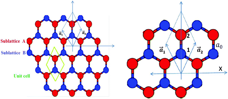 |
| | Fig. 1 A schematic presentation of a graphene sheet. Each Bravais lattice unit cell includes two nonequivalent sites, which are denoted by A and B. A blown-up image of the unit cell is shown separately; a1 and a2 are the primitive vectors. | |
Pure graphene, though extremely interesting, suffers from zero band gap fixation, which makes it uninteresting from a device application point of view. The development of graphene-based electronics depends on our ability to open a tunable band gap. Various approaches have been developed to fabricate high-performance graphene devices by engineering their band gaps so as to improve their semiconducting properties. One of the approaches is evidently to choose N and B and substitute them to replace C atoms to form ‘carbon alloys’. The atomic masses of these dopants are closest to carbon, which would seemingly be acceptable for carbon lattices to adjust to, whilst at the same time significantly altering the electronic properties of the host material because of the electron-rich and electron-deficient nature of N and B atoms. Experimental and theoretical studies on graphene doping do show this possibility of making p-type and n-type semiconducting graphene. In fact, studies by different means, like doping with heteroatoms,7 doping with metal contacts,8 chemical functionalization,9 applying electric fields and depositing graphene on substrates like SiC and SiO2,10 have shown this possibility. Band gap opening using p-type doping using Al, boron, H, tetracyanoethylene (TCNE) and n-type doping using N, P and S has been studied in the past.7,11–14 The observation has been that the dopant atoms can modify the electronic band structure of graphene and open up an energy gap between the valence and conduction bands. Recently, an ab initio study of the different dopant interactions in the host graphene has also been reported, which provides useful information on the behavior of dopants.15 While Lherbier et al.11 studied the charge mobilities and conductivity of the system by doping graphene with different concentrations of B and N impurities (up to 4%) randomly (without studying the band gap), Wu et al.12 studied the band gap opening in graphene by only single atom doping of B and N whereas Xiaohui et al.16 have studied the band gap opening in graphene by B/N codoping. Fan et al.17 have studied graphene/boron nitride hetero-bilayers to tune the band gap, whereas X. Fan et al.18 have primarily focused on boron–nitride combination as a dopant and changing the concentration by taking a larger number of host atoms. Manna et al.19 have shown that the patching of graphene and h-BN sheet with semiconducting and/or insulating BxNy (Cz) nanodomains of various geometrical shapes and sizes (h-BN sheet) can significantly change the electronic and magnetic properties. Despite all such work, a systematic study of exact role of concentration and position of dopant atoms in modulating the band gap has still not appeared in the literature.
In the present paper, we have made an effort to present a systematic study of the effect of substitutional doping of boron and nitrogen in the graphene sheet by slowly increasing the concentration of doping and also considering the different isomers of the same doped configuration. We choose both B and N atoms for our study, using each individually as the dopant due to their nearly similar size to that of carbon and because of their electron-deficient and electron-rich characters, respectively, and deferring for the present time using a combination of B and N in host of C atoms. In the following, we outline computational details for our approach of using density functional theory and describe the results for B and N doping in Section 3. These results are discussed and finally concluded in Section 4.
2. Computational details
Graphene is known to relax in a 2-D honeycomb structure (Fig. 1) and the B and N doped graphene will be assumed to have a similar starting structure and be subject to energy minimization considerations to calculate new bond lengths. To do this analysis, geometry optimizations and electronic structure calculations have been performed using the VASP (Vienna Ab initio Simulation Package)20,21 code based on density functional theory (DFT). The approach is based on an iterative solution of the Kohn–Sham equation22 of the density function theory in a plane-wave set with the projector-augmented wave pseudopotentials. In our calculations, the Perdew–Burke–Ernzerhof (PBE)23 exchange–correlation (XC) functional of the generalized gradient approximation (GGA) is adopted. The plane-wave cutoff energy was set to 400 eV. The optimizations of the lattice constants and the atomic coordinates are made by the minimization of the total energy. The 5 × 5 supercell (consisting of 50 atoms) has been used to simulate the isolated sheet and the sheets are separated by larger than 12 Å along the perpendicular direction to avoid interlayer interactions. The Monkhorst–Pack scheme is used for sampling the Brillouin zone. In the calculations, the structures are fully relaxed with a Gamma–centred 7 × 7 × 1 k-mesh. During all of the calculation processes, except for the band determination, the partial occupancies were treated using the tetrahedron methodology with Blöchl corrections.24 For band structure calculation, partial occupancies for each wavefunction were determined using the Gaussian smearing method with a smearing of 0.01 eV. For geometry optimizations, all of the internal coordinates were relaxed until the Hellmann–Feynman forces were less than 0.005 Å.
3. Results and discussion
First of all, a pure graphene sheet was fully optimized, including its lattice constant, which was found to be 2.45 Å, which is slightly less than the experimental value of 2.46 Å, and the resulting C–C bond length of pure graphene is 1.41 Å, which is in agreement with previous results.25 The lattice constants, a1 and a2, (refer to Fig. 1) are expressed in Cartesian coordinates as
where ao is the interatomic distance or C–C bond length and has been found to be close to 1.42 Å.
Then, the band structure of pure graphene was calculated and presented in Fig. 2, which is also found to be in agreement with the literature,2 indicating thereby the reliability of computational procedure.
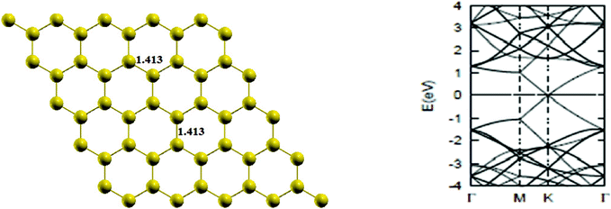 |
| | Fig. 2 The optimized geometry and band structure of a pure graphene sheet. The bond length is in Å. The Fermi level in the band structure is set to zero. | |
Subsequently, pure graphene was doped with an increasing concentration of boron and nitrogen atoms. The relaxed lattice constant of doped graphene increases in the case of B and decreases in the case of N, with an increase in the number of doped atoms because the covalent radius of boron is larger than a carbon atom and that of nitrogen is less than carbon. This is consistent with the earlier results, as summarized in the Introduction.
We study six B-doped, as well as N-doped, configurations with 2%, 4%, 6%, 8%, 10% and 12% concentration of doping.
3.1 Boron doping
As pointed out earlier, a boron atom is likely to adjust to surrounding C atoms of the host (see Fig. 3). Therefore, when a graphene sheet is doped with one boron atom, the boron atom also undergoes sp2 hybridization and, due to the nearly same size of C and B, no significant distortion in the 2-D structure of graphene is expected, except for a change in adjoining bond length. As a result, a bond length is found to expand to 1.48 Å. Using the computational procedure as stated above, it is possible to calculate the electronic properties, especially the band structure. Of interest are the K-points along special directions of the Brillouin zone and we find that the linear dispersion near the Dirac point is not destroyed. However, due to the electron-deficient character of boron, the Fermi level shifts significantly by about 0.7 eV below the Dirac point, resulting in p-type doping. Another important observation that can be made is regarding breaking of the symmetry of two graphene sublattices because of the introduction of a B atom, now introducing an energy gap of 0.14 eV around the Dirac point. This changes the behavior of graphene from semi-metal to conductor. The charge transfer was also calculated using Bader charge analysis, which shows 1.79 e charge transfer from boron to carbon. The results are in agreement with earlier calculations.12 Some data concerning a single atom doping by B is presented in Table 1.
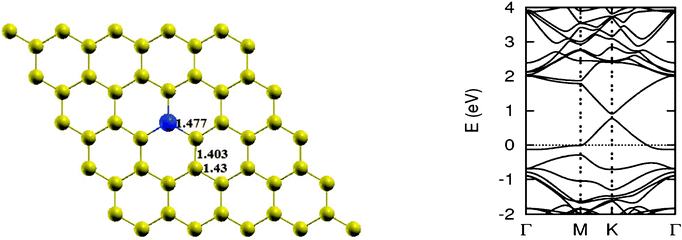 |
| | Fig. 3 The optimized geometry and band structure of a single boron atom doped graphene sheet. The blue ball denotes a boron atom. | |
Table 1 Some parameters affecting single atom doping by a boron atom
| Parameter |
d
B–C (Å) |
Band gap (eV) |
Charge transfer (e) |
| Our work |
1.48 |
0.14 |
−1.79 |
|
Ref. 12
|
1.49 |
0.14 |
−1.84 |
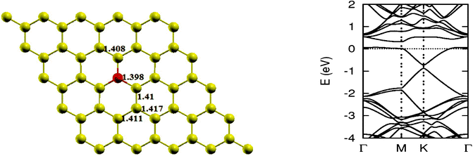
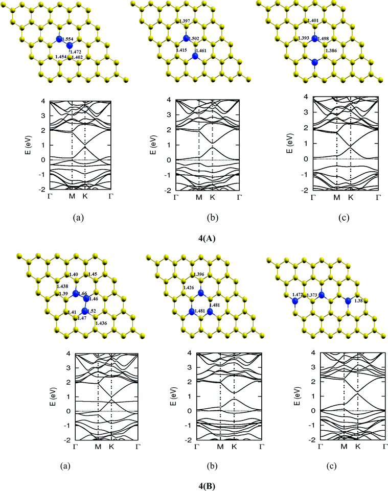
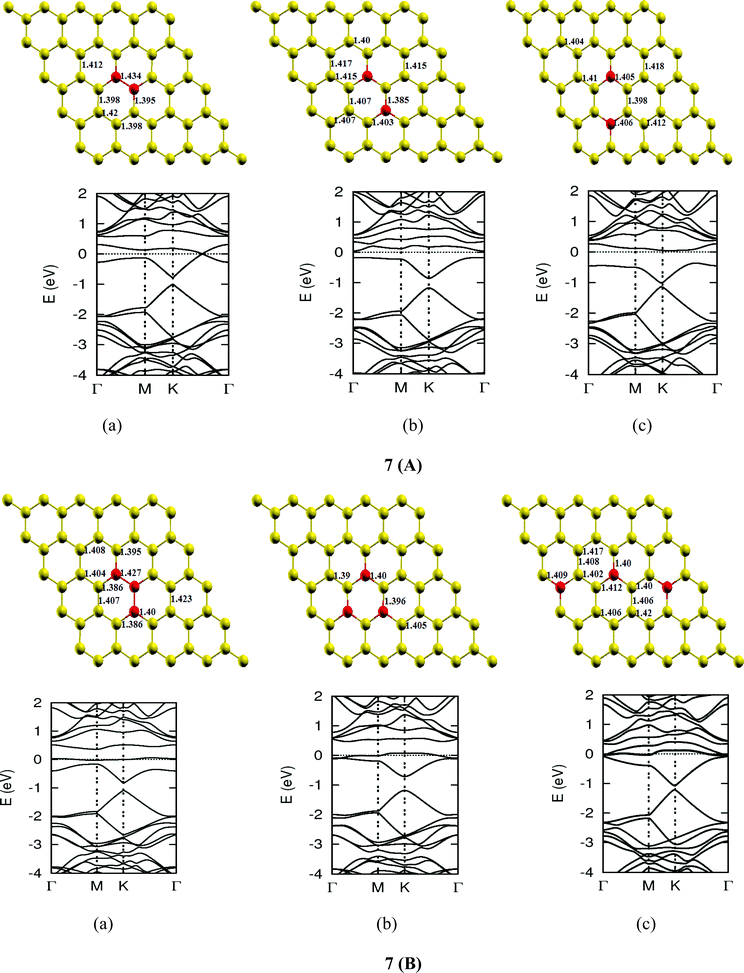
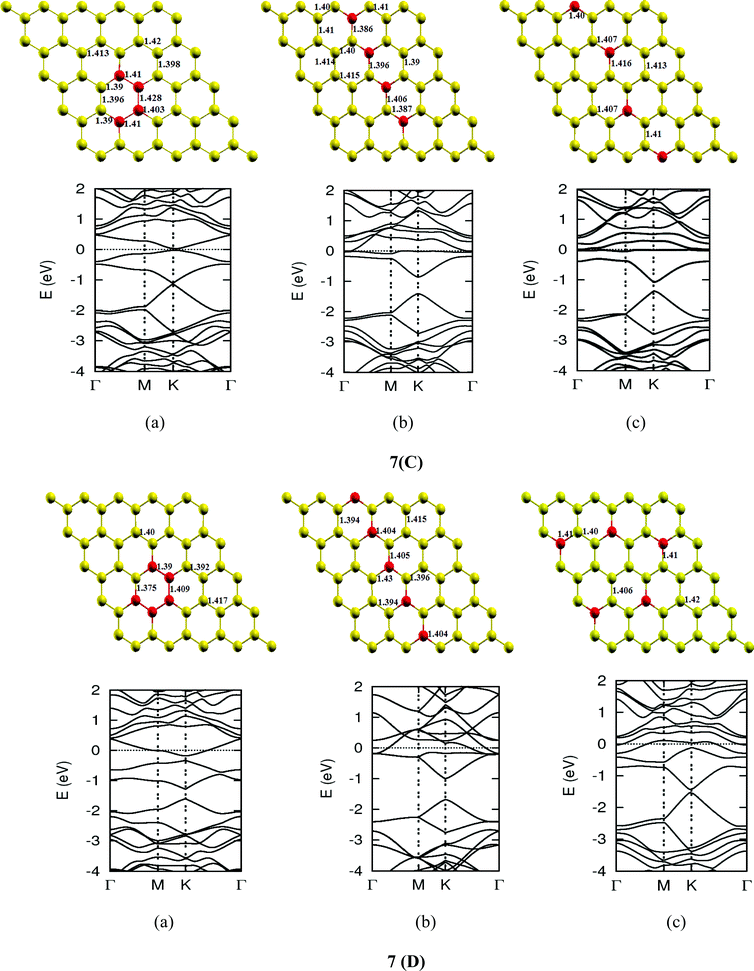
Once we found a satisfactory reproduction of the results as obtained for pure graphene and single atom doped boronated graphene, we carried out our calculations with an increasing number of dopants, also taking into account different sites of doping for the same concentration. It can be observed that several isomers of the same atomic concentrations doped graphene become possible. These isomers differ significantly in cohesive energy, bond length and band gap. Although we calculated several possible isomers for concentrations of dopants (2%, 4%, 6%, 8%, 10% and 12%), for the sake of brevity, we present here in Fig. 4 only a few isomers with the configurations of mainly three doping sites i.e. when all of the dopant atoms are adjacent, when they are at the same sublattice positions (either A or B) and finally when they are at different lattice positions i.e. one dopant atom is placed at sublattice A and other is at B.
 |
| | Fig. 4-1 | |
 |
| | Fig. 4-2 | |
 |
| | Fig. 4-3 Some optimized geometries and band structures of two, three, four, five and six B atom doped graphene sheet in (A), (B), (C), (D) and (E), respectively. The upper rows in these show geometrical structures and bottom rows present the band structures. | |
The investigations of structural properties show the shrinkage of C–C bond lengths which fall in proximity to B dopants. This possibly results from longer C–B bond lengths because of the larger covalent radius of B than C and preservation of the structure. This also results in disorder of the lattice when the dopants are placed at adjacent positions. The data regarding changes in bond lengths can be read from the structural part of the figures presented in Fig. 4.
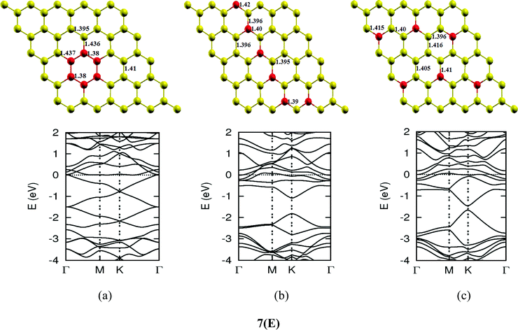
As we can see from the band structures in Fig. 4(A–E) the maximum band gap develops on doping for the category (b) isomer. This category originates from when the dopants are placed at the same sublattice positions (either A or B) as defined in Fig. 1. This observation reinforces our belief that the origin of band gap is due to symmetry breaking of graphene sublattices, which maximizes itself in these configurations. The electronic structure analysis shows that band gap in general increases with an increase in concentration of doping. In Fig. 5, we give a separate plot of this variation of band gap with % concentration of doped B atoms for the configuration (b), which shows the largest band gap.
 |
| | Fig. 5 Band gap in increasing order of doping concentrations for a boron doped graphene sheet. The isomers with highest band gap are chosen. | |
The effect of concentration of B atoms also affects band structure details. The effects are prominently different for an odd number of dopants as compared to an even number of dopants. From Fig. 4, if we examine configurations (a) for varying B-atom concentrations, the band structure of the doped graphene is highly deformed, especially in the case of configurations containing an odd number of dopants, where a linear dispersion relation at the Dirac point is also affected. This can result from deviation from a crystalline structure on doping. The linear dispersion in graphene is due to its crystal structure and when the dopants are placed at adjacent positions in configuration (a), the structure is highly distorted, which results in deformation of the band structure. Also, as can be seen from the band structure plots for this category, the band gap is less for configurations with an even number of dopants than those with an odd number of dopants (the band gap is completely closed in six atom doped in one hexagon). This is possibly due to the symmetry formed by the hetero-atoms in the two triangular sublattices (see Fig. 4(C) and (E)).
When the nitrogen atom is doped into the graphene sheet, similar effects to those in the case of boron are observed. It also interacts through sp2 hybridization with the C atom. The bond length of three N–C bonds formed is 1.40 Å and there is almost no distortion in the planar structure of graphene. But due to the electron-rich character of the resulting structure, the Fermi level shifts by 0.7 eV above the Dirac point. Also, like B, due to breaking of the symmetry of the graphene sublattices, the system shows a band gap of 0.14 eV. Bader charge analysis shows a charge transfer of 1.16 e from carbon to nitrogen.12 Some data of single N atom doped graphene for comparison with other calculations is provided in Table 2. We present the optimized structure, as well as the electronic band structure of some isomers obtained by doping an increasing number of N atoms in Fig. 6.
Table 2 Some parameters affecting single atom doping by a nitrogen atom
| Parameter |
d
N–C (Å) |
Band gap (eV) |
Charge transfer (e) |
| Our work |
1.40 |
0.14 |
1.16 |
|
Ref. 12
|
1.42 |
0.14 |
1.12 |
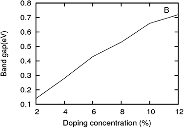
The lattice and band structure resulting from various number of dopants of N atom are shown in Fig. 7. The structural properties of N-doped graphene geometries do not show any remarkable change because of nearly same size of covalent radius of carbon and nitrogen. The trend in electronic properties is similar to that of boron doped graphene, except for the fact that the Fermi energy is shifted above the Dirac point. A plot of the variation of band gap with doping concentration is shown in Fig. 8, which is for the configuration in which the maximum band gap is introduced. Thus B and N doping provides a way to introduce a gap in graphene at the Dirac point to a significant value without changing the unique properties of graphene. In Table 3, we summarize the important results from doping both B and N atoms.
 |
| | Fig. 7-1 | |
 |
| | Fig. 7-2 | |
 |
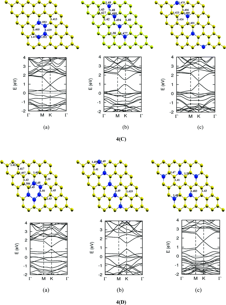
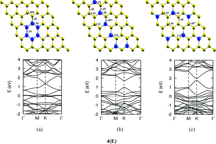
| | Fig. 7-3 Optimized geometries and band structures of two, three, four, five and six N atom doped graphene sheet in (A), (B), (C), (D) and (E), respectively. The upper rows in these show geometrical structures and bottom rows present the band structures. | |
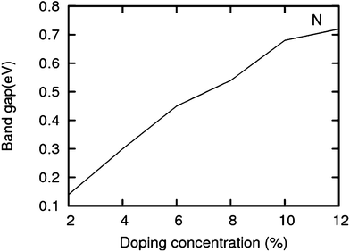 |
| | Fig. 8 Band gap in increasing order of doping concentrations (for the configuration having a maximum band gap) for N. | |
Table 3 Cohesive energy and Band gap for increasing doping concentration and various possible configurations a, b, c, as described in corresponding figures
| Concentration (%) |
Configuration (B doped) |
E
coh
(eV/atom) |
Band gap (eV) |
Configuration (N doped) |
E
coh
(eV/atom) |
Band gap (eV) |
|
E
coh = [Etot − niEi]/n (i = C, B, N).
|
| 2 |
|
−9.13 |
0.14 |
|
−9.16 |
0.14 |
| 4 |
a |
−9.03 |
0.15 |
a |
−9.10 |
0.19 |
| b |
−9.05 |
0.28 |
b |
−9.12 |
0.30 |
| c |
−9.06 |
0.14 |
c |
−9.13 |
0.15 |
| 6 |
a |
−8.94 |
0.19 |
a |
−9.04 |
0.19 |
| b |
−8.96 |
0.43 |
b |
−9.08 |
0.45 |
| c |
−8.98 |
0.17 |
c |
−9.07 |
0.16 |
| 8 |
a |
−8.85 |
0.02 |
a |
−8.99 |
0.04 |
| b |
−8.88 |
0.53 |
b |
−9.03 |
0.54 |
| c |
−8.87 |
0.28 |
c |
−9.02 |
0.30 |
| 10 |
a |
−8.76 |
0.28 |
a |
−8.93 |
0.32 |
| b |
−8.81 |
0.66 |
b |
−8.99 |
0.68 |
| c |
−8.82 |
0.14 |
c |
−9.02 |
0.13 |
| 12 |
a |
−8.64 |
0.00 |
a |
−8.84 |
0.003 |
| b |
−8.73 |
0.72 |
b |
−8.94 |
0.72 |
| c |
−8.72 |
0.23 |
c |
−8.97 |
0.22 |
From several structural curves presented here for multi-atom B and N doped graphene, one notices a pattern of changes in some adjoining bond lengths with typical signature of boron different from that of nitrogen. Furthermore, the band gaps continue to grow with increasing doping concentrations. The electronic band structure data has been summarized in Table 3. In Table 3, Ecoh is the cohesive energy per atom of B- or N-doped configuration graphene and Etot and Ei represent the total energies of a structure and of individual elements present within the same supercell, respectively. ni is the number of species i present in the configuration, which could be C, B or N, while n is the total number of atoms present in a supercell (n = 50). However, with increasing concentration of dopants the cohesive energy decreases, indicating the decreasing structural stability compared to the pristine graphene sheet (Ecoh = −9.20 eV per atom). Also, the N-doped configurations show larger negative values of cohesive energy than their boron counterparts. This is due to the nearly similar size of the atomic radius of C and N, which results in lesser structural disorder in comparison to B, as is clear from bond length values.
4. Summary and conclusions
Density functional theory was used to study the geometry and electronic structure of boron and nitrogen doped graphene sheets. The effect of doping was investigated by varying the concentrations of dopants from 2% (one atom of the dopant in 50 host atoms) to 12% (six dopant atoms in 50 atoms host atoms) and also by considering different doping sites for the same concentration of substitutional doping. By B and N doping, p-type and n-type doping is induced, respectively, in the graphene sheet. While the planar structure of the graphene sheet remains unaffected on doping, the electronic properties change from semi-metal to semiconductor with an increasing number of dopants. It has been observed that isomers formed by choosing various doping sites differ significantly in the stability, bond length and band gap introduced. The observation is that the electronic properties of a graphene lattice depend upon symmetry and hence positioning of dopant atoms plays a significant role in modulating the band gap. The band gap is at a maximum when dopants are placed at same sublattice positions (A or B) in adjacent sublattices of graphene due to the combined effect of symmetry breaking of sublattices and the band gap is closed when dopants are placed at adjacent positions (alternate sublattice positions). These interesting results provide the possibility of designing the band gap of graphene as required, allowing its application in a wide range of electronic devices by controlling the system geometry. Indeed, it would not be out of place to mention that the role of N and B doping has also found favor26 in replacing platinum-based cathodes for polymer-based electrolytic fuel cells (PEFCs).
Acknowledgements
We express our gratitude to the VASP team for providing the code, the computing facilities at IUAC (New Delhi) and the departmental computing facilities at Department of Physics, PU, Chandigarh. PR wishes to acknowledge UGC for financial support. VKJ acknowledges support from CSIR as Emeritus Scientist. He also acknowledges support of Alexander von Humboldt Foundation, Germany for extending the research visit when this work got completed.
References
- K. S. Novoselov, A. K. Geim, S. V. Morozov and D. Jiang, Science, 2004, 306, 666–669 CrossRef CAS.
- A. K. Geim and K. S. Novoselov, Nature Mater., 2007, 6, 183–191 CrossRef CAS.
- A. K. Geim, Science, 2009, 324, 1530–1534 CrossRef CAS.
- P. Avouris, Z. Chen and V. Perebeinos, Nat. Nanotechnol., 2007, 2, 605 CrossRef CAS.
- A. H. Castro Neto, F. Guinea, N. M. R. Peres, K. S. Novoselov and A. K. Geim, Rev. Mod. Phys., 2009, 81, 109–162 CrossRef CAS.
- D. R. Cooper, B. D'Anjou, N. Ghattamaneni, B. Harack, M. Hilke, A. Horth, N. Majlis, M. Massicotte, L. Vandsburger, E. Whiteway and V. Yu, ISRN Condensed Matter Physics, 2012, 2012, 501686 CrossRef.
- P. A. Denis, Chem. Phy. Lett., 2010, 492, 251–257 CrossRef CAS.
- G. Giovannetti, P. A. Khomyakov, G. Brocks, V. M. Karpan, J. van den Brink1 and P. J. Kelly, Phys. Rev. Lett., 2008, 101, 026803 CrossRef CAS.
- X. Wang, X. Li, Y. Yoon, P. K. Weber, H. Wang, J. Guo and H. Dai, Science, 2009, 324, 768–771 CrossRef CAS.
- P. Shemella and S. K. Nayak, Appl. Phys. Lett., 2009, 94(032101), 3pp Search PubMed.
- A. Lherbier, R. X. Blasé, Y. Niquet, F. Triozon and S. F. Roche, Phys. Rev. Lett., 2008, 101, 036808 CrossRef.
- M. Wu, C. Cao and J. Z. Jiang, Nanotechnology, 2010, 21(505202), 6pp Search PubMed.
- J. M. García-Lastra, Phys. Rev. B, 2010, 82, 235418 CrossRef.
- Y. H. Lu, W. Chen, Y. P. Feng and P. M. He, The Journal of Physical Chemistry B Letts., 2009, 113, 2–5 CrossRef CAS.
- N. Al-Aqtash, M. Al-Tarawneh Khaldoun, T. Tawalbeh and I. Vasiliev, J. App. Phys., 2012, 112, 034304 CrossRef.
- Xiaohui Deng, Yanqun Wu, Jiayu Dai, Dongdong Kang and Dengyu Zhang, Phys. Letts. A, 2011, 375, 3980–3894 Search PubMed.
- Yingcai Fan, Mingwen Zhao, a Zhenhai Wang, Xuejuan Zhang and Hongyu Zhang, App. Phys. Lett., 2011, 98, 083103 CrossRef.
- Xiaofeng Fan, Zexiang Shen, A. Q. Liu and Jer-Lai Kuo, Nanoscale, 2012, 4, 2157 RSC.
- K. Manna Arun and K. Pati Swapan, J. Phys. Chem. C, 2011, 115, 10842–10850 Search PubMed.
- G. Kresse and J. Furthmüller, Phys. Rev. B, 1996, 54, 11169 CrossRef CAS.
- G. Kresse and J. Furthmüller, Comput. Mat. Sci., 1996, 6, 15 CrossRef CAS.
- W. Kohn and L. J. Sham, Phys. Rev. 140 A, 1965, 1133–1138 Search PubMed.
- J. P. Perdew and K. E. Burke, Phys. Rev. Lett., 1996, 77, 3865–3868 CrossRef CAS.
- P. E. Blöchl, O. Jepsend and O. K. Andersen, Phys. Rev. B, 1994, 49, 16223 CrossRef.
- A. L. E. Garcia, S. E. Baltazar, A. H. Romero, J. F. Perez Robels and A. Rubio, Journal of Computational and Theoretical Nanoscience, 2008, 5, 1–9 CrossRef.
- Zhufeng Hou, Xianlong Wang, T. Ikeda, K. Terakura, M. Oshima, M.-i. Kakimoto and S. Miyata, Phys. Rev. B, 2012, 85, 165439 CrossRef.
Footnote |
| † Present address: Department of Theoretical Chemistry, Technical University, D-10623 Berlin, Germany. |
|
| This journal is © The Royal Society of Chemistry 2013 |
Click here to see how this site uses Cookies. View our privacy policy here.