
Identifying chemical and physical changes in wide-gap semiconductors using real-time and near ambient-pressure XPS
 a
Rachel E.
Cross,
a
Martin W.
Allen,
c
Pilar
Ferrer,
e
Georg
Held,
e
D. Andrew
Evans
*a
a
Rachel E.
Cross,
a
Martin W.
Allen,
c
Pilar
Ferrer,
e
Georg
Held,
e
D. Andrew
Evans
*a
Abstract
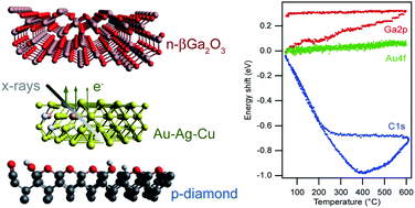
Photoelectron spectroscopy is a powerful characterisation tool for semiconductor surfaces and interfaces, providing in principle a correlation between the electronic band structure and surface chemistry along with quantitative parameters such as the electron affinity, interface potential, band bending and band offsets. However, measurements are often limited to ultrahigh vacuum and only the top few atomic layers are probed. The technique is seldom applied as an in situ probe of surface processing; information is usually provided before and after processing in a separate environment, leading to a reduction in reproducibility. Advances in instrumentation, in particular electron detection has enabled these limitations to be addressed, for example allowing measurement at near-ambient pressures and the in situ, real-time monitoring of surface processing and interface formation. A further limitation is the influence of the measurement method through irreversible chemical effects such as radiation damage during X-ray exposure and reversible physical effects such as the charging of low conductivity materials. For wide-gap semiconductors such as oxides and carbon-based materials, these effects can be compounded and severe. Here we show how real-time and near-ambient pressure photoelectron spectroscopy can be applied to identify and quantify these effects, using a gold alloy, gallium oxide and semiconducting diamond as examples. A small binding energy change due to thermal expansion is followed in real-time for the alloy while the two semiconductors show larger temperature-induced changes in binding energy that, although superficially similar, are identified as having different and multiple origins, related to surface oxygen bonding, surface band-bending and a room-temperature surface photovoltage. The latter affects the p-type diamond at temperatures up to 400 °C when exposed to X-ray, UV and synchrotron radiation and under UHV and 1 mbar of O2. Real-time monitoring and near-ambient pressure measurement with different excitation sources has been used to identify the mechanisms behind the observed changes in spectral parameters that are different for each of the three materials. Corrected binding energy values aid the completion of the energy band diagrams for these wide-gap semiconductors and provide protocols for surface processing to engineer key surface and interface parameters.
- This article is part of the themed collection: Photoelectron spectroscopy and the future of surface analysis
 Please wait while we load your content...

