
Printable and flexible integrated sensing systems for wireless healthcare
Kemeng
Zhou†
,
Ruochen
Ding†
,
Xiaohao
Ma
and
Yuanjing
Lin
 *
*
School of Microelectronics, Southern University of Science and Technology, Shenzhen 518055, China. E-mail: linyj2020@sustech.edu.cn
First published on 23rd February 2024
Abstract
The rapid development of wearable sensing devices and artificial intelligence has enabled portable and wireless tracking of human health, fulfilling the promise of digitalized healthcare applications. To achieve versatile design and integration of multi-functional modules including sensors and data transmission units onto various flexible platforms, printable technologies emerged as some of the most promising strategies. This review first introduces the commonly utilized printing technologies, followed by discussion of the printable ink formulations and flexible substrates to ensure reliable device fabrication and system integration. The advances of printable sensors for body status monitoring are then discussed. Moreover, the integration of wireless data transmission via printable approaches is also presented. Finally, the challenges in achieving printable sensing devices and wireless integrated systems with competitive performances are considered, so as to realize their practical applications for personalized healthcare.
 Yuanjing Lin | Yuanjing Lin received her Ph.D degree in Electronics and Computer Science from the Hong Kong University of Science and Technology in 2018. From 2019 to 2020, she was a Postdoctoral Fellow in Electrical Engineering and Computer Sciences at the University of California, Berkeley. She is currently an Assistant Professor at the Southern University of Science and Technology. Her research interests focus on nanomaterial innovation for wearable and printable electronics, micro/nanostructured sensors, flexible energy storage devices and their applications in smart systems. |
1. Introduction
Sensors play a crucial role in converting targeted analytes into measurable electric signals, making them a vital tool in medical care and health monitoring.1–8 The rapid development of a large library of functionalized sensors has enabled the widespread utilization of wearable sensors over the past few decades.9–13 In addition, wireless transmission technologies have evolved to achieve high-speed data transfer. The most widely used wireless technologies for wearable sensors are Radio Frequency Identification (RFID),14–16 Near Field Communication (NFC),14,17,18 and Bluetooth.19,20 The combination of wearable sensors and wireless communication modules enables pervasive sensing and interconnection of physical objects via the wearable Internet of Things (IoT).21–23 Integrated wireless sensor systems are qualified to collect data from subjects and the local environment and transmit them to remote devices for further data analytics and visualization.24,25 These systems have a range of applications in health monitoring, environmental detection and artificial intelligence, bringing great convenience to human life.Printing technologies, including screen printing, roll-to-roll (R2R) printing, inkjet printing and three dimensional (3D) printing, have been widely adopted to realize wearable sensing devices and antenna systems.26–34 These printable fabrication procedures provide the advantages of relatively low cost, high throughput, and desirable compatibility with various functional materials and platforms. For instance, the antenna for near field communication (RFID) wireless data transmission can be prepared on textiles, plastics, and other substrates with versatile designs on antenna patterns in a straightforward manner using printing technologies. This approach enables the integration of wireless communication modules into wearable devices, providing new opportunities for real-time monitoring and data transmission.
This review focuses on recent research progress in printable sensing systems with wireless data transmission (Fig. 1). Section 2 provides an overview of printing technologies for wearable electronics. Section 3 discusses the commonly utilized printable materials and their unique properties, while section 4 provides a summary of printable substrates as wearable platforms. Afterwards, section 5 presents the recent advances in printable physical and chemical sensors and their applications for smart sensing. In section 6, the design and printable fabrication of antennas for wireless data transmission are discussed, followed by the advances of integrated wireless sensing systems for real-time and remote monitoring presented in section 7. Finally, section 8 discusses challenges and research prospects for printable sensing devices with wireless data transmission. The advances in printing technologies provide a cost-effective and versatile approach for the fabrication and integration of sensors and multifunctional modules for a wide range of applications, including healthcare, environmental monitoring, and smart cities.
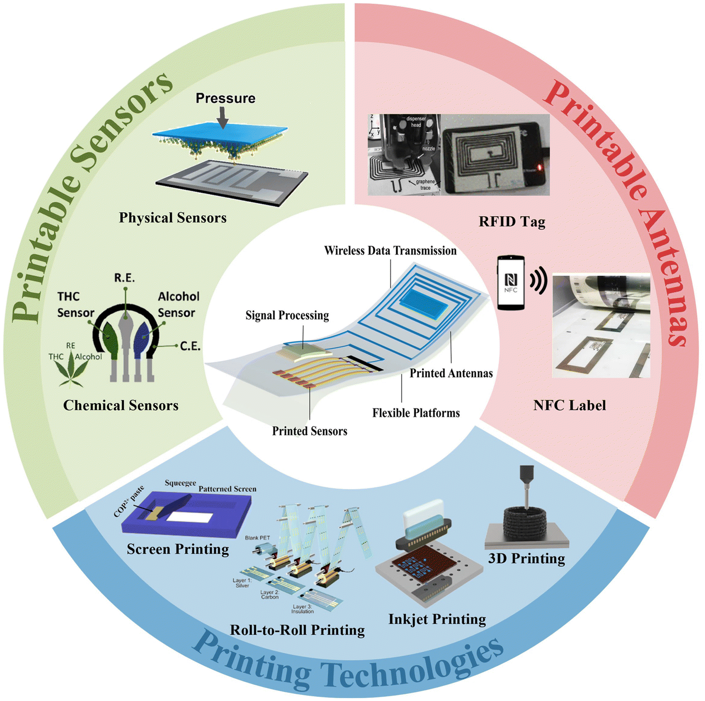 | ||
| Fig. 1 The most commonly adopted technologies and electronic configurations for printable sensing systems with wireless data transmission. Screen printing. Reproduced from ref. 35 with permission from [Springer Nature], copyright [2020]. Roll-to-roll printing. Reproduced from ref. 36 with permission from [American Chemical Society], copyright [2018]. Inkjet printing. Reproduced from ref. 37 with permission from [John Wiley and Sons], copyright [2019]. 3D printing. Reproduced from ref. 38 with permission from [Elsevier], copyright [2022]. Physical sensors. Reproduced from ref. 39 with permission from [American Chemical Society], copyright [2019]. Chemical sensors. Reproduced from ref. 40 with permission from [Elsevier], copyright [2020]. An RFID tag. Reproduced from ref. 41 with permission from [Springer Nature], copyright [2022]. An NFC label. Reproduced from ref. 42 with permission from [John Wiley and Sons], copyright [2021]. | ||
2. Printable technologies for integrated sensing systems
Printing techniques have been widely employed in device fabrication and integrated systems for sensing applications. Printable sensing systems can be designed for various platforms with the attractive factors of versatile configuration, compatibility of different substrates and facile integration. This section provides a summary of the major printing methods for sensor devices, including screen printing, inkjet printing, R2R printing, and 3D printing technologies. In general, each printing method has unique properties, including printing speed, resolution, ink viscosity, printed film thickness and substrate adaptability. The selection of the appropriate printing method depends on the specific requirements of device fabrication, including the type of sensor, the substrate materials, and the desired properties. Table 1 provides a summary and comparison of the key factors for different printing technologies.43| Screen printing | R2R printing | Inkjet printing | 3D printing | |
|---|---|---|---|---|
| Resolution (μm) | >50 | >0.05 | >0.5 | >30 |
| Printing speed (m min−1) | ∼70 | ∼1000 | ∼1 | ∼4 |
| Mask | Yes | Yes | No | No |
| Substrate geometry | Flat | Flat | Irregular | Irregular |
| Ink properties | High viscosity and shear thinning | Low viscosity | Low viscosity, long-term stability, and small particle size | Shear thinning, and low solvent content |
| Advantages | Fast fabrication, low-cost, and high-throughput | High printing speeds and high throughput | Precise control, low materials waste, and low-cost | High aspect ratios and printed layer thicknesses; 3D geometries |
| Disadvantages | Low-resolution | High cost and space requirement | Nozzle clogging and limited types of inks | Relatively low resolution |
2.1. Screen printing
Screen printing is a popular printing process that uses porous stencils to transfer ink onto a substrate. The screen, squeegee, and substrate play key roles in the printing process. The printable area of the screen, usually made of porous mesh fabric and nylon, is always open, allowing ink to pass through, while the non-printable area is blocked off by a hardened photosensitive material.26,51,52 The masks act as image carriers and ink metering systems throughout the printing process, setting minimum feature sizes and deposition thicknesses. As shown in Fig. 2a, the printing inks are pressed down onto the substrates through the masks under squeegee pressure.53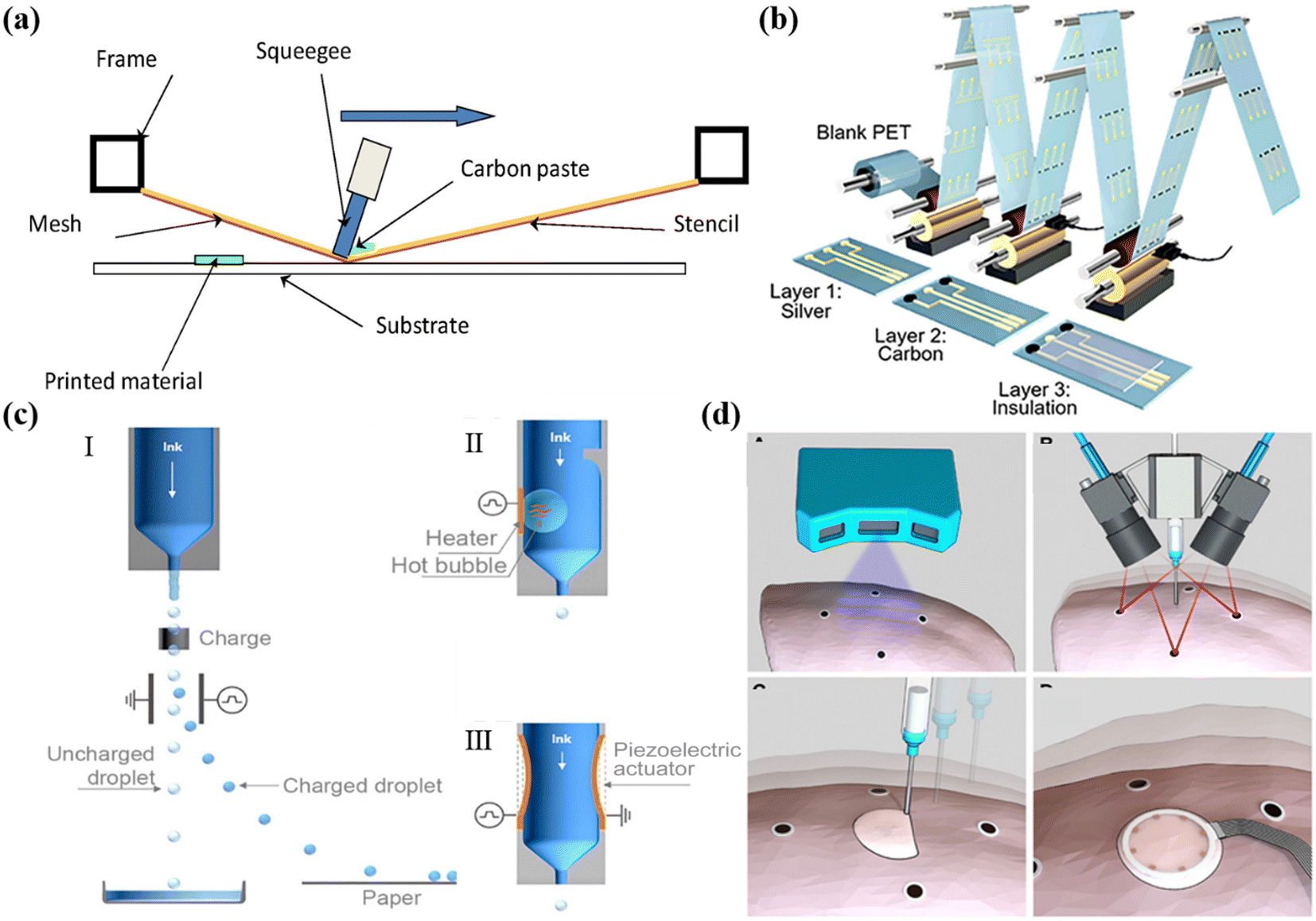 | ||
| Fig. 2 Printing technology of sensors. (a) Schematic demonstration of screen printing. Reproduced from ref. 53 with permission from [Elsevier], copyright [2016]. (b) R2R gravure printed electrochemical sensors. Reproduced from ref. 36 with permission from [American Chemical Society], copyright [2018]. (c) Continuous inkjet printing (I) and drop-on-demand inkjet printing (thermal inkjet (II) and piezoelectric inkjet (III)). Reproduced from ref. 66 with permission from [American Chemical Society], copyright [2020]. (d) Direct 3D printing of sensors on pig lungs. Reproduced from ref. 81 with permission from [American Association for the Advancement of Science], copyright [2020]. | ||
Without strict requirements on the physical and chemical properties of the printing materials, screen printing provides superior compatibility for device fabrication on different flexible platforms. It is a versatile technology that can be used for large-scale production on different substrates, including fabrics and polymers. It is suitable for printing materials with high concentrations or large particle sizes. It serves as one of the most affordable and facile methods for preparing conductive electrode patterns and functional layers. Thus, it has been widely adopted for fabricating devices based on layer-by-layer thin-film architectures, such as sensors, batteries and optoelectronics. However, the disadvantages lie in the relatively high material waste and low patterning resolution, which limit the device performance enhancements, especially for those that require minimized patterning line width/interspaces and highly precise control of the film thickness. Besides, since it requires masks for patterning, and direct contact between the applied masks and printed layers is unavoidable, the construction of high performance sensing devices with strict requirements on the printed film quality and functional layer interfaces can be limited.
2.2. R2R printing
R2R printing is a typical solution-based process applied to large-scale and mass manufacturing of devices. It employs additive and subtractive processes to fabricate structures with high throughput and low cost.51,54,55 Among different types of R2R printing processes, gravure and flexographic printing are two of the representative technologies to achieve high-throughput patterning.In gravure printing, printed patterns are firstly constructed on the surface of the gravure cylinder in the form of an engraved intaglio grid, which is then directly transferred to substrates by physical contact ink deposition.56,57 It allows pattern reproduction with variable depth and size, providing compatibility for a variety of substrates. In flexographic printing, functional inks are transferred to the anilox roller, followed by the removal of excess ink in the non-image area by blades. In this way, the pattern can then be completely transferred to the flexographic printing plate.57 Compared to screen printing, R2R printing exhibits higher printing speeds, resolution, and fabrication reproducibility. Thus, it enables large scale and high-throughput patterns and device manufacture. For instance, Javey and Cho et al. demonstrated R2R gravure printing of electrodes on flexible substrates in a scale of up to 150 m. The as-printed electrodes showed remarkable consistency in conductivities, which can then be functionalized into sensors with reproducible performances for promising applications in health monitoring (Fig. 2b).36 Lee et al. manufactured comb-structured acceleration sensors on PET in a scalable fashion by R2R gravure printing. The sensors are based on sandwich device architectures including the Ag bottom electrode, the barite barium sulfate (BaSO4) dielectric layer and the Ag top electrode. To avoid the stiction problem, the Ag top electrodes were printed on the water-soluble PVP sacrificial layer and then transferred on top of the dielectric layer.58 Javey et al. achieved electrochemical sensors with remarkable performance reproducibility for wearable and medical devices via R2R printing.59
2.3. Inkjet printing
Inkjet printing is a non-contact printing technology that can be categorized into two main methods: continuous inkjet printing (CIJ) and drop-on-demand (DOD) inkjet printing (Fig. 2c).60–66 During CIJ printing, the nozzles continuously produce droplets, while in DOD inkjet printing, droplets are only ejected when the appropriate signal is received. DOD inkjet printing can generate pressure pulses that control the formation and ejection of inks.To achieve the precise control of ink jetting during DOD, thermal and piezoelectric cartridges are commonly adopted. In thermal inkjet printing, the inks are heated by a heating element, which results in bubble formation followed by rapid expansion and collapsion.67 The bubble explosion creates the driving power that ejects the ink from the nozzle.64,65,68 However, the high temperature process limits the choice of printing materials and substrates, and can also affect the printing stability and device performance. In contrast, piezoelectric inkjet printing applies voltage pulses to a piezoelectric actuator, which deforms the actuator and causes the nozzle to eject droplets.64,65,68–70 By changing the pulse pressure, piezoelectric inkjet printers can realize the desirable precise control of the droplet speed. Normally the cartridges for inkjet printing allow droplets in the volumes of 1 pL to several tens of pL. Thus, piezoelectric inkjet printing exhibits desirable form factors of high patterning resolution, precise materials mass loading, enhanced ink stability and low pollution. Thus, it has been widely adopted for the fabrication of micro-sensors, in which high resolution electrodes and precise control of functional materials’ mass loading play a critical role in ensuring high sensing performances. However, the printing speed can be relatively low compared to other methods, and thus might not be preferred for industrial level applications. Besides, to avoid nozzle clogging issues, it requires efforts on the synthesis of inks with rational optimized viscosity, high stability and uniform particle size. For instance, it normally requires low-viscosity inks with small particle sizes to ensure smooth printing, which to some extend limits the material's compatibility, such as nanowires and 2D materials.
2.4. 3D printing
3D printing is another type of drop-on-demand process in which materials are printed layer by layer in an additive manner based on digitally controlled material deposition. It has become increasingly popular for the fabrication of sensors attributed to its advantages of low material waste, mass fabrication, versatile customization, rapid prototyping, and facile procedures.71,72 Among different types of 3D printing, direct ink writing (DIW), fused deposition modeling (FDM), selective laser sintering (SLS), stereolithography (SLA) are the most commonly adopted strategies.73–76 Typically, DIW refers to the direct extrusion of a fluid material through a nozzle to form the desired shape, while FDM involves melting and extruding a thermoplastic filament through a nozzle to form the desired shape. Polymers and composite inks with high viscosities or that can be pre-synthesized into solid-state filaments are mainly utilized. To further broaden the material library for functional device construction and geometry resolution, laser-assisted 3D printing methods are introduced. SLS utilises lasers to sinter powdered materials such as metals and polymers to form the desired shapes, while SLA realizes light sensitive materials that solidify a liquid layer by layer.Attributed to the facile and versatile construction of irregular architectures, a variety of integrated sensing devices have been demonstrated.77–79 For example, Kim and co-workers developed 3D-printed flexible sensors for ion sensing integrated into a flexible microfluidic patch for wearable sweat sensing.80 Moreover, 3D printing allows direct device fabrication on non-planar substrates, such as biological surfaces. Recently, McAlpine et al. realized in situ 3D-printed sensors on porcine lungs for tissue surface deformation mapping based on electrical impedance tomography. Such an adaptive 3D printing approach provides an innovative strategy to construct implantable medical devices (Fig. 2d).81
3. Formulas of printable inks for sensing devices
The printable inks used for preparing sensors and integrated devices typically consist of solvents, functional micro/nano materials, conductive fillers, binders, and additives.60,82,83 The solvents contribute to dissolving or dispersing active components and modifying the ink viscosity, while the binders minimize the intermolecular interaction between fillers, improving their stability and shelf life. Additives help prevent nanoparticle agglomeration, ensuring a smooth printing process. The functional conductive fillers largely affect the ink conductivity, which is one of the most critical factors for the performance enhancement of the printed devices. It is worth mentioning that the printable ink formula, especially the composition of functional materials and solvents, may differ widely depending on specific applications. For most printed sensors and integrated systems, decent conductivities of electrodes and interconnects are highly desirable to ensure electron transfer. Therefore, the most commonly used conductive fillers, including metal, carbon-based and conductive polymer materials, will be discussed in this section.3.1. Metallic inks
Metal inks are a popular choice for printed electrode contacts and interconnects due to their relatively higher electrical conductivity when compared to other types of inks.84 There are various commercially available metallic-based inks based on silver (Ag), gold (Au), and copper (Cu), while the ink formulas can directly affect the electrical and mechanical properties of the printed sensor systems.However, most of the flexible substrates cannot withstand high temperature processing. Research efforts have been devoted to investigating the potential methods to print Ag patterns with desirable conductivity without high temperature annealing.93 Wu et al. developed Ag nanodendrites with a specific branching structure for printable inks (Fig. 3a).90 The branching structure can form an interconnected network and allows sintering at a relatively low temperature of 80 °C to achieve high conductivity. This method would inspire the fabrication of printed sensors and integrated systems in a cost-effective and time-efficient manner, while minimizing the risk of flexible substrate damage.
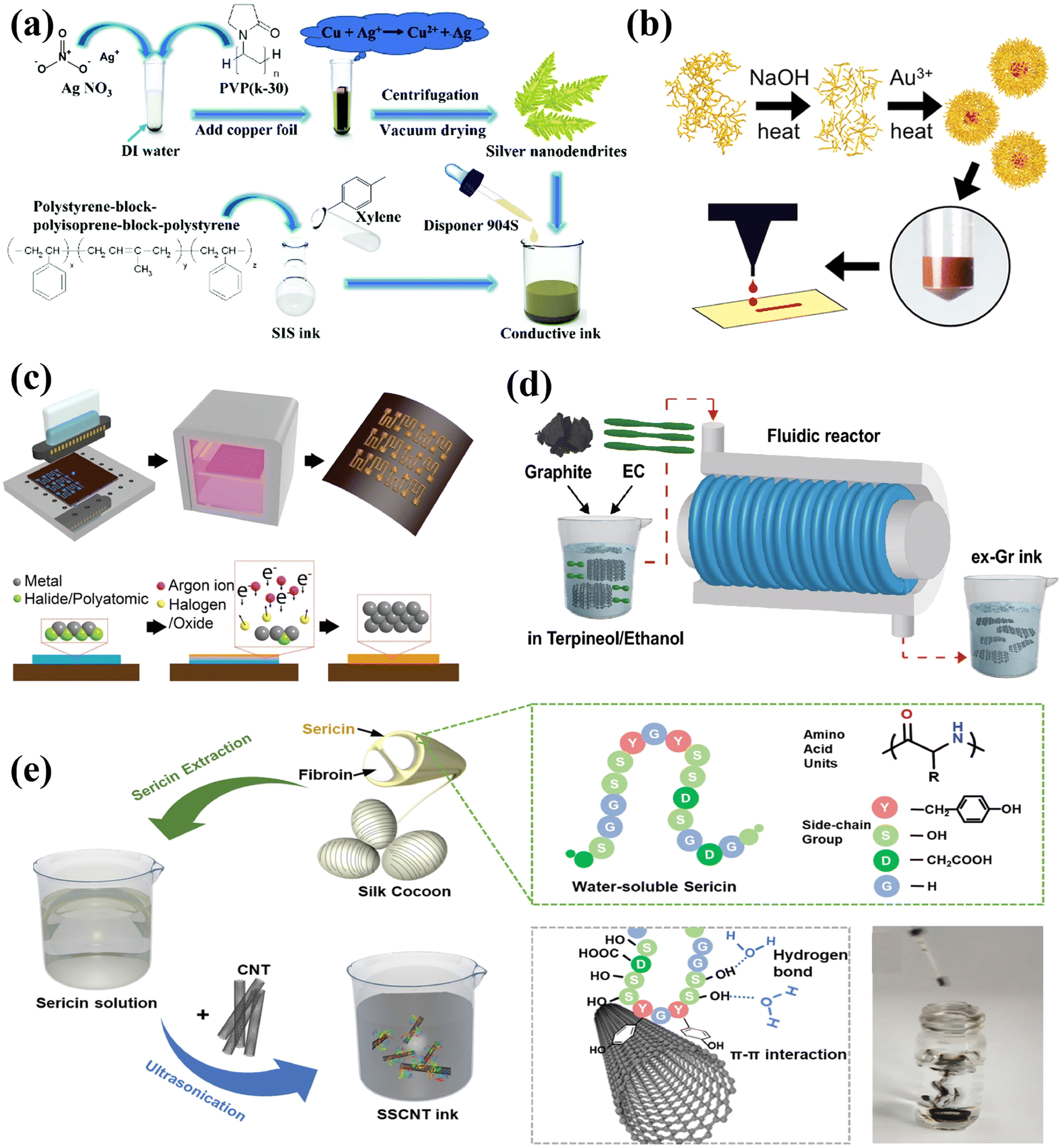 | ||
| Fig. 3 Preparation strategies of conductive printable inks. (a) Silver-based ink (Ag ND) with a special branch structure. Reproduced from ref. 90 with permission from [the Royal Society of Chemistry], copyright [2019]. (b) Microwave heating was used for both the controlled starch hydrolysis and AuNP synthesis. Reproduced from ref. 95 with permission from [American Chemical Society], copyright [2018]. (c) The non-equilibrium plasma transforms the metal ink into a metal structure at low temperatures. Reproduced from ref. 37 with permission from [John Wiley and Sons], copyright [2019]. (d) A high-concentration conductive ink based on defect-free graphene through a scalable hydrodynamic process. Reproduced from ref. 115 with permission from [Springer Nature], copyright [2021]. (e) Stable and biocompatible CNT ink stabilized by sustainable silk sericin. Reproduced from ref. 117 with permission from [John Wiley and Sons], copyright [2020]. | ||
The species and concentrations of reducing agents can affect the size, shape, and yield of gold nanoparticles.94,95 It has been reported that starch molecules can be hydrolyzed to control further growth and produce gold nanoparticle solutions with controllable and stable sizes. The starch solution is heated and hydrolyzed in sodium hydroxide (NaOH) to activate its reducing end, which reduces the Au ions in the solution to Au0.95,96 Based on this approach, Enriquez et al. realized stable and high yield synthesis of Au NPs by fine-tuning the size of starch granules, coupled with microwave-assisted synthesis (Fig. 3b).95 Another classic approach to prepare Au fillers with controllable morphologies is the seed-mediated growth method, in which Au3+ ions are normally reduced by sodium citrate.97 Mazali et al. adopted the seed-mediated approach for preparing Au nanosphere colloids with high uniformity.
To reduce the cost, Au-based composite inks provide alternative choices. He et al. recently developed a convenient method for growing highly conductive gold nanowires on carbon nanofibers (CNFs).98 By regulating the reduction kinetics of Au(III) precursors and preventing nanoparticle fusion, Au nanocrystals undergo monomer-by-monomer attachment of Au (0) monomers onto the facets of Au crystals, resulting in the formation of a single-crystalline structure on CNFs. The resulting Au NW/CNF inks also show remarkable conductivity and stability for printable device fabrication.
To address this issue, the oxidation resistance of Cu NPs can be improved by isolating the copper core from oxidizing substances with an oxidation-proof shell.99–103 Jeong et al. enhanced the chemical resistance of Cu NP particle membrane-based electrodes by covering the surface of Cu NPs with a Ni protective shell.104 The electrical conductivity and oxidation resistance of the Cu@Ni electrode were improved by varying the thickness of the Ni shell. In addition to the Cu–Ni core–shell structure, the Cu–Ag core–shell structure has also been synthesized to prevent the oxidation of Cu particles.105
In general, the metal nanoparticles have a high particle density and surface free energy, which can lead to ink agglomeration. Thus, it is a common practice to apply stabilizers to prepare homogeneous inks.37 Alternatively, particle-free inks with better storage stability might need to reduce the precursors to metals by thermal annealing after the printing process. However, the annealing could potentially deform the substrate.86,106 To tackle this challenge, Zorman et al. have developed an inkjet printing technique that uses particle-free inks made from inorganic metal salts. These inks are transformed into metallic structures by nonequilibrium plasma at low temperatures (138 °C), as depicted in Fig. 3c.37 Electrons from the plasma or secondary electrons released from the thin film reduce the metal cations to crystallize the metal. When metal salts are dissociated in the presence of ions, metal cations become available.
3.2. Carbon-based materials
Carbon-based materials, particularly graphite, graphene, and carbon nanotubes (CNTs), provide considerate and tunable conductivity, as well as superior chemical stability. Thus, tremendous research efforts have been devoted to the development of carbon-based ink formulas for multi-functional printable electronics.To address these issues, hydrokinetic-based graphite exfoliation methods were applied to directly exfoliate graphite using suitable solvents and water to produce defect-free graphene sheets with large lateral dimensions.112,114 Based on such scalable hydrodynamic strategies, Choi et al. developed a conductive ink based on defect-free graphene with a high-concentration of 47.5 mg mL−1 (Fig. 3d).115 Besides, electrochemical exfoliation is also a commonly adopted method for preparing graphene. Parvez et al. recently demonstrated a water-based inkjet printable ink made from electrochemically exfoliated graphene (ECG) in a time-efficient manner.116 The inkjet printable inks containing more than 75% monolayer and multilayer graphene flakes were achieved using a core electrochemical stripping method. Two graphite foils as the anode and cathode were biased at a direct current (DC) voltage of 10 V for stripping in a 0.5 M (NH4)2SO4 electrolyte. These methods contribute to the synthesis of high-quality graphene inks for printed electronics.
By introducing functional groups to the CNT surface or as reaction sites for subsequent modifications, CNTs can be dispersed in water and organic solvents with improved uniformity. Zhang et al. used silk sericin as a stabilizer to prepare stable and biocompatible CNT inks (Fig. 3e).117 The formation of sericin–CNT hybrids with a core–sheath structure modifies the surface properties of CNTs and stabilizes their homogeneous dispersion. The prepared inks deliver decent compatibility to various printing methods and substrates. Mariatti et al. prepared stable and environmentally friendly water-based inks by dispersing multi-walled carbon nanotubes (MWCNTs) in an aqueous solution with the help of biopolymer surfactants Gum Arabic (GA).118 The hydrophobic tail of GA adsorbs on the surface of MWCNTs, and the hydrophilic end extends into the water. Thus, the barrier between nanotubes can be formed to reduce aggregation.
In summary, carbon-based materials offer desired electrical conductivity and chemical inertness, enabling wide applications in composite ink formulas to construct printed electrodes for a variety of sensors.
3.3. Conductive polymer materials
Conductive polymers are another commonly adopted material for sensor fabrication due to their feasibility for preparing various printable formulations and functionalization via doping. Among various conductive polymers, poly(3,4-ethylenedioxythiophene):poly(styrene sulfonate) (PEDOT:PSS), and polyaniline (PANI) are two of the most commonly utilized materials in the construction and design of flexible and stretchable electrodes. Given their desirable biocompatibility, and electrical conductivity, together with reliable mechanical and electrochemical stability, a variety of printable inks for flexible sensing device and system fabrication have been reported.50,119–122![[thin space (1/6-em)]](https://www.rsc.org/images/entities/char_2009.gif) 000 cycles at 30% strain. Apart from these, PEDOT-based inks have been used for conductive interconnects for multi-functional device/chip integration.127–130
000 cycles at 30% strain. Apart from these, PEDOT-based inks have been used for conductive interconnects for multi-functional device/chip integration.127–130
4. Flexible substrates for printable electronics
One of the most attractive advantages of printable electronics lies in their capability to various flexible substrates. To realize high-performance electronics, it requires careful matching of printing techniques, printable inks and rationally modified surface properties of the flexible substrates. In this section, recent advances in preparing printable sensors on different flexible substrates and platforms will be discussed.4.1. Polymer substrates
Flexible substrates based on polymers such as polyethylene terephthalate (PET), polyimide (PI) and stretchable elastomers are the most widely adopted platform for flexible and wearable electronics. This is mainly due to their relatively smooth surface morphologies and tunable properties for precise pattern printing, as well as excellent robustness and deformability.Printable sensors for temperature, pressure, and electrochemical analyte monitoring have been well developed on PET substrates. For instance, Javey et al. realized high-throughput fabrication of sensor electrodes, microchannel patterned spacers and packing layers based on PET substrates by combining R2R printing and laser cutting. By stacking the three layers vertically, sweat sensing patches can be prepared in a facile manner (Fig. 4a).59 The prepared microfluidic sensor patch can be applied to real-time monitoring of the sweat rate and analytes such as sodium, potassium and glucose, which can provide critical information for personalized healthcare. While the fabrication strategies for printable sensors and systems on PET are quite mature, the flexible patches suffer from non-stretchable and less conformal contact with skin.
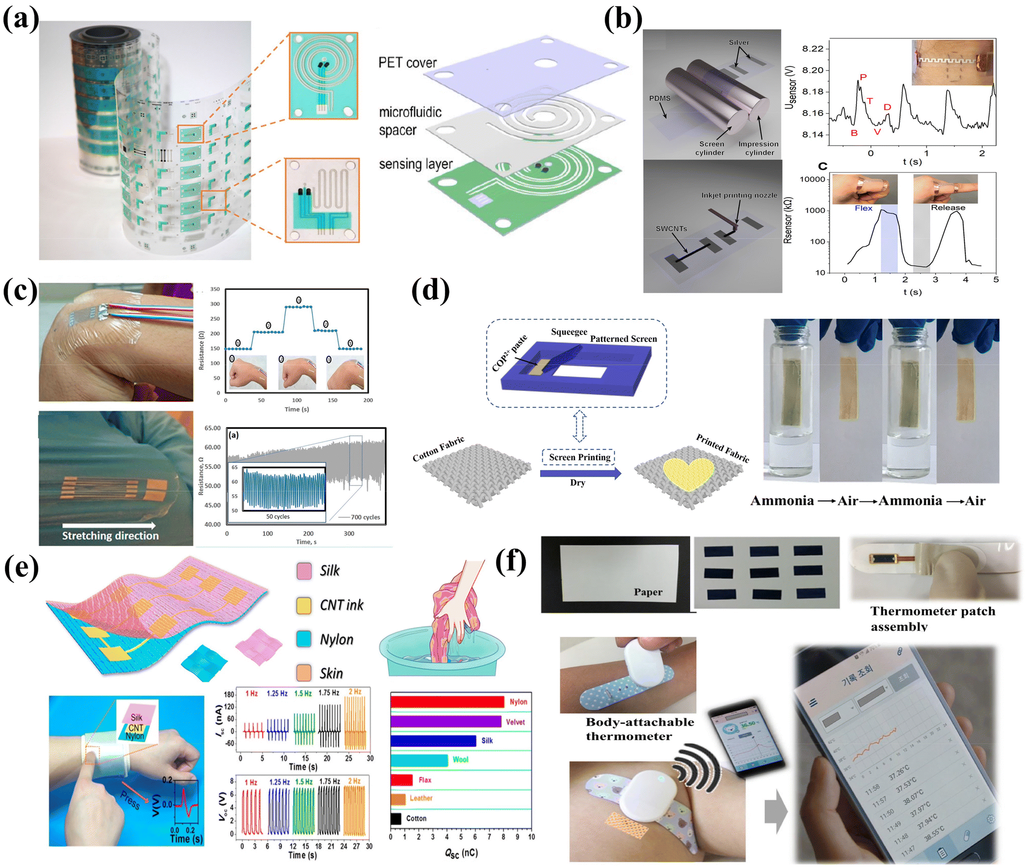 | ||
| Fig. 4 The substrate of the print sensor. (a) The sweat sensor is fabricated on the PET substrate by R2R printing. Reproduced from ref. 59 with permission from [American Association for the Advancement of Science], copyright [2019]. (b) R2R printing technology prepares a highly sensitive piezoresistive strain sensor on a PDMS substrate. Reproduced from ref. 138 with permission from [American Chemical Society], copyright [2021]. (c) Wearable strain sensor on a medical bandage. Sensors based on medical bandages have good stability in 700 cycles of repeated bending and stretching. Reproduced from ref. 141 with permission from [American Chemical Society], copyright [2019]. (d) Screen-printed preparation of a multiresponsive fabric sensor with photochromic and thermochromic capabilities. Reproduced from ref. 35 with permission from [Springer Nature], copyright [2020]. (e) Screen-printed washable tribo-sensors on textiles for intelligent human–machine interactions. Reproduced from ref. 143 with permission from [American Chemical Society], copyright [2018]. (f) The high-sensitivity paper temperature sensor can be carried as a bar thermometer. The sensor is suitable for the human body's wearable health monitoring. Reproduced from ref. 144 with permission from [Elsevier], copyright [2020]. | ||
Stretchable elastic substrates provide enhanced mechanical stability to withstand deformation and improved skin contact comfort, which are particularly desired for E-skin sensing applications. Among various elastic substrates, polydimethylsiloxane (PDMS) with excellent flexibility, chemical resistance, and heat resistance emerges as one of the popular choices. It also shows good compatibility with different printing methods and inks, enabling versatile electrodes and sensing array fabrication. For instance, piezoresistive strain sensor arrays with high sensitivity can be prepared on an R2R patterned stretchable PDMS–Ag substrate with inkjet printed CNTs as sensing layers (Fig. 4b).138 Wang et al. prepared PDMS-based sensors for wearable electrocardiography (ECG) and photoplethysmography (PPG) through inkjet printing, which can clearly detect the pulsating nature of blood in the tissue.127
Apart from these, other polymer-based substrates, including polyimide (PI), thermoplastic polyurethane (TPU),139 and Kapton,140 have also been utilized as flexible platforms for printable sensors. For instance, ultra-thin and adhesive commercial medical tapes can serve as skin-conformable substrates for sensor integration. These medical tapes are normally made of a thin polyurethane (PU) film coated with an acrylic adhesive and can be seamlessly applied on the human skin. By using aerosol jet printing to allow lower temperature sintering of the silver nanoparticle ink, Yeong et al. prepared a wearable strain sensor on such medical tapes to realize efficient capture of strain response signals from the body (Fig. 4c).141 The printed sensors exhibit remarkable stability during repeated bending and stretching, which shows promising potential for remote clinical applications.
4.2. Textiles
Textiles are considered as one of the competitive candidates for skin-friendly sensing devices due to their flexibility and permeability with superior wearing comfort. Textiles are typically categorized into fibers, yarns, and fabrics. Fibers, with high length to diameter ratios, can be twisted to form threads or yarns.142 Fabrics are defined as layered structures of fiber materials made from yarns, utilizing techniques such as weaving and knitting. Various conductive materials, including metals, conductive polymers, and carbon materials, have been employed to produce conductive fibers, which can then be further functionalized into sensing devices. To prepare textile-based sensors in a printable manner, screen printing is the commonly adopted approach. Mao et al. prepared e-textiles with photochromic, thermochromic, and ammonia sensing functionalities by screen-printing a viologen polymer made from cyclotriphosphazene onto cotton textiles (Fig. 4d).35While screen printing provides a facile and scalable strategy to prepare sensors on textiles, it is found that the printed dense layers would sacrifice the air and moisture permeability of the textiles. Moreover, the relatively high viscosity of screen printing inks could bind the fibers into bundles and lead to cracks or materials delamination with mechanical interferences. Utilizing active materials to form interaction with the fibers can be a promising approach to realize e-textiles with mechanical stability under harsh deformation or even the washing process. Wang et al. demonstrated screen printed triboelectric touch/gesture sensing textile based CNTs (Fig. 4e).143 Due to the interaction between CNTs and fiber networks, the e-textiles display desirable sensitivity for intelligent human–machine interfacing application, while maintaining permeability and washability.
Another concern for printable sensor fabrication on textiles lies in the limited patterning resolution mainly due to the capillary effects along the rough fiber surfaces and networks, which hinder device miniaturization and integration with microelectronic modules. It remains a challenge to achieve high-resolution and versatile pattering on textiles while maintaining their permeability and flexibility. Recently, Ma and co-workers reported a monolithically integrated in-textile sensing wristband by combining polymer-assisted metal deposition and the optimized lithography method with printed masks.12 The developed integrated system in a single piece of textile consists of multifunctional modules, including the ion-selective sensor, signal processing circuit and Bluetooth wireless transmission, so as to realize epidermal sweat biosensing. The proposed strategy would provide a new perspective for textile sensing bioelectronics.
Overall, textiles offer a skin-friendly flexible platform for sensing devices with their original porous structure, permeability, and wearing comfort. To realize practical applications in wearable fitness monitoring and point-of-care healthcare, research efforts are expected to further enhance the patterning resolution and reliable encapsulation. Thus, e-textiles could exhibit competitive electrical conductivity, mechanical robustness and waterproofness compared to other flexible devices.
4.3. Paper-based substrates
Paper has the advantages of low price, light weight, biodegradability, and recyclability. Most importantly, its surface roughness lies between polymers and textiles which makes it the most widely used platform for printing with a long history.144,145 Lee et al. prepared sensors on paper that can simultaneously measure relative humidity, temperature, and compression bending through inkjet printing.144 This high-sensitivity temperature sensor is suitable for use in smart packaging labels and disposable biosensors, and can also be carried around as a band thermometer (Fig. 4f). Impressively, the paper-based sensor shows a temperature sensing sensitivity of up to 658.5 Ω °C−1. The research advances in paper-based printable electronics will no doubt contribute to the wide applications of cost-effective and disposable sensors, especially for clinical quick tests.However, papers normally cannot withstand stretching/twisting, and could have severe deformation with moisture/liquid. Therefore, rational packing designs are necessary for practical uses.
5. Printable sensors for bio-signal acquisition
With proper matching of printing methods, functional inks and flexible substrates, multifunctional sensors for bio-signal acquisition can be constructed in versatile designs. Similar to sensors prepared in conventional methods, printable sensors can also be categorized into physical and chemical sensors.5.1. Physical sensors
Physical sensors are devices that utilize specific physical phenomena to convert the physical quantities being measured into electrical signals. The linear correlation between the input and output signals can be used for signal decoding. In this section, we will mainly discuss pressure, strain and temperature sensors, which are the most widely frequently reported printable sensors.Pressure sensors can be applied for human activity tracking which can be estimated with the regional pressure and strain variations. 3D-printed hydrogel pressure sensors have been extensively researched due to their ease of preparation, excellent sensitivity, and mechanical strength. Guo et al. utilized a hydrogel with a self-healing function to create a 3D-printed sensor capable of monitoring human movement (Fig. 5a).146 The hydrogel exhibited excellent self-healing function, remarkable stretchability, and stable recovery characteristics. Apart from the unique self-healing properties, other attractive factors of hydrogel sensors include biocompatibility, while the water loss could affect the sensor stability. Thus, skin-friendly and moisture-absorbing 3D-printed hydrogel pressure sensors that prevent water loss and preserve its performance are highly desirable. Yin et al. designed an ionic conductor through 3D printing (Fig. 5b).147 The highly transparent, stretchable, and elastic hydrogel was then transformed into a capacitive sensor capable of detecting pressure and strain.
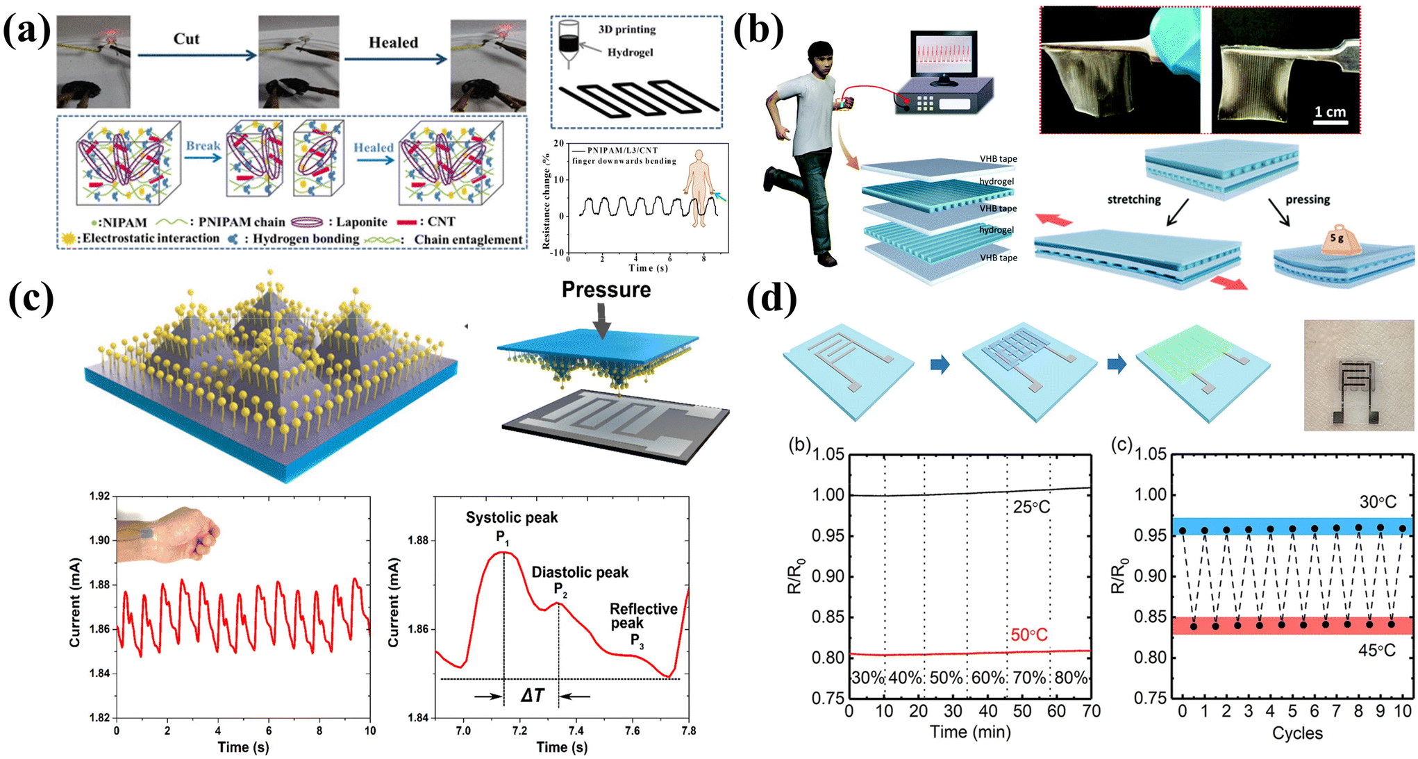 | ||
| Fig. 5 Printable physical sensors for human activity and health monitoring. (a) The self-healing hydrogel is used to prepare a pressure sensor that can monitor human movement through 3D printing. Reproduced from ref. 146 with permission from [American Chemical Society], copyright [2019]. (b) A high-sensitivity ion skin sensor was designed by 3D printing. Reproduced from ref. 147 with permission from [Royal Society of Chemistry], copyright [2019]. (c) Pressure sensor based on inkjet printed Ag NP electrodes and a special pyramid microstructure. Reproduced from ref. 39 with permission from [American Chemical Society], copyright [2019]. (d) Fully printed temperature sensor with a wide sensing range. Reproduced from ref. 153 with permission from [Springer Nature], copyright [2020]. | ||
Another practical application of flexible pressure sensors is for health monitoring such as pulse sensing. The pulse waveform includes shock waves (P waves), tidal waves (T waves), and diastolic waves (D waves). Flexible pressure sensors applied onto human skin can extract the output variation under different pulse waves from deep tissues and distant sites, such as the digital artery and dorsalis pedis artery.148,149 Due to the relatively small pressure signals generated by pulses, highly sensitive pressure sensors are required. Cheng et al. developed a pressure sensor with a fast response time and high sensitivity by combining inkjet printed Ag NP electrodes and conductors using a special pyramidal microarray structure (Fig. 5c).39 The pressure sensor can detect arterial pulses and is suitable for wearable bio-diagnostics and therapy. Changes in deformation and pressure alter the contact area between the conductor and the printed electrodes of the pyramidal structure, resulting in a distinct signal response.
Apart from pulse sensing, motion tracking is another key application for flexible and printable sensors. Strain sensors can monitor the structural strain changes during human activities. For example, Tokito et al. fabricated a fully printed flexible strain sensor based on ferroelectric polymers. The sensor was utilized for wearable bending sensing on human fingers.150 Zhang et al. patterned flexible strain sensors using MWCNTs/PDMS composite ink through screen printing. The printed sensors exhibited a high gauge factor of 1.55, demonstrating excellent linearity of up to 100% deformation. The sensors showcased robust sensing stability, and rapid dynamic response, enduring over 4000 strain cycles without degradation. These strain sensors are employed in wearable electronic devices for applications such as motion detection, exercise and rehabilitation training, as well as structural health monitoring.151
Temperature sensors fabricated via printing methods have also gained widespread attention due to the soaring demand, especially during the pandemic. Huang et al. proposed a strategy for the direct synthesis of molybdenum disulfide (MoS2) patterns on a polymer substrate using inkjet printing. The patterned MoS2 serves as a temperature sensor for accurate epidermal temperature tracking.152 Wang et al. developed a fully printed temperature sensor with a detection range of 25 °C to 50 °C and remarkable humidity stability (Fig. 5d).153 The addition of a (3-glyceroyloxypropyl) trimethoxysilane (GOPS) crosslinker and fluorinated polymer passivator (CYTOP) significantly improved the humidity stability and temperature sensitivity of the PEDOT:PSS base membrane. By integrating printed sensors into the printed flexible hybrid circuit, real-time body temperature monitoring was achieved in a stable and reliable manner.
5.2. Chemical sensors
Chemical sensors are typically used for gas detection and biomarker analysis and convert analyte concentrations into quantified current or voltage signals.154 Chemical sensors have been widely applied in clinical medicine, environmental monitoring, biotechnology, the food industry and agriculture.5,155Printable fabrication of chemical sensors can provide the desirable scalability, reproducibility and cost-effectiveness, especially for disposable rapid biosensing strips. One of the most widely adopted printed platforms for chemical detection in liquid samples is the screen printed three-electrode PET patch. It normally consists of two carbon-based patterns as working and counter electrodes, and one Ag pattern serves as the reference. One of the carbon-based electrodes can be functionalized with bio-receptors and other active materials so as to achieve selective and sensitive analyte detection.
A variety of printable chemical sensors for on-site rapid drug sensing, such as fentanyl, have also been reported on screen printed platforms, which can be prepared in a scalable manner (Fig. 6a).156 In another work, Wang et al. presented a wearable electrochemical sensor device for rapid on-site saliva testing (Fig. 6b).40 The device included shared counter and reference electrodes, and two printed selective sensing electrodes for dual analyte detection. Both THC and alcohol can be detected in saliva samples within three minutes with the printable sensing patch, demonstrating their potential applications in roadside driver screening.
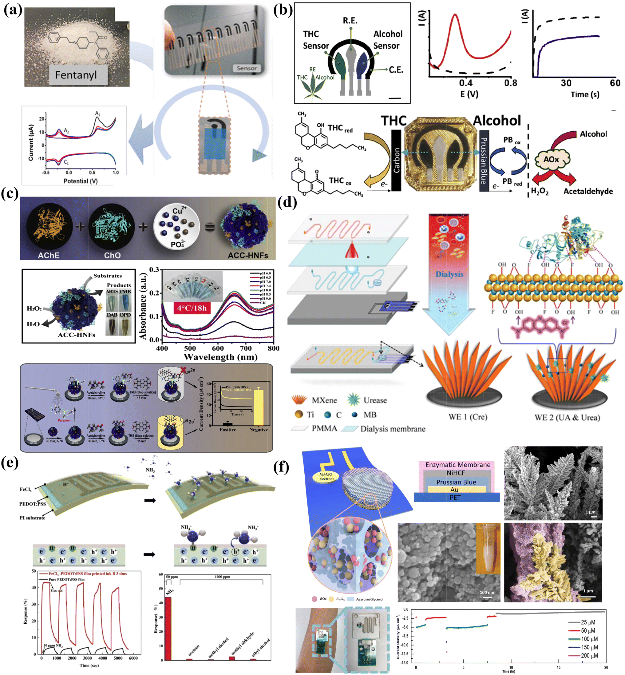 | ||
| Fig. 6 Printable chemical sensors for analytes’ rapid/on-site testing and their performance enhancements with nanomaterials. (a) Scalable fabrication of on-site illegal drug fentanyl sensors. Reproduced from ref. 156 with permission from [American Chemical Society], copyright [2019]. (b) Saliva sensing patch for on-site THC and alcohol dual analyte detection. Reproduced from ref. 40 with permission from [Elsevier], copyright [2020]. (c) Paper-based organophosphorus pesticide sensor with ultrasensitivity based on enzyme-inorganic hybrid nanoflowers and can generate electrochemical/colorimetric signals simultaneously. Reproduced from ref. 157 with permission from [Elsevier], copyright [2019]. (d) MXene-based screen-printed electrodes with a dialysis microfluidic chip for blood analytes monitoring without extra pretreatment. Reproduced from ref. 158 with permission from [John Wiley and Sons], copyright [2018]. (e) Inkjet printing of a PEDOT:PSS thin film with FeCl3 additives for high performance ammonia gas sensing. Reproduced from ref. 159 with permission from [Elsevier], copyright [2019]. (f) Nanostructured glucose sensor with reliable long-term stability prepared on printed sweat sensing platforms. Reproduced from ref. 154 with permission from [John Wiley and Sons], copyright [2019]. | ||
Nevertheless, printable sensors normally exhibit non-competitive sensitivity and stability. One of the main reasons is limited surface areas with printed layers in the thin film morphology. It fails to facilitate interaction between analytes and sensitive materials, and the rapid charge accumulation at the interfaces would also lead to signal drifting. The other possible reason is that printed dense films can be easily delaminated especially in liquid sample analysis, which leads to device failures. Thus, it requires efforts to develop printable sensors with high sensitivity and stability for reliable and continuous sensing, such as portable contamination detection and wearable healthcare.
Researchers have proposed innovative printable strategies to combine with nanomaterials as to construct sensing devices for real-time and continuous biomarker monitoring with high accuracy and reliability. For example, Lu et al. successfully designed all-in-one enzyme-inorganic hybrid nanoflowers and immobilized on paper-based printed electrodes for on-site organophosphorus pesticide analysis. The sensor is capable of dual signal readings, including the electrochemical current output and colorimetric response, and delivers ultrahigh sensitivity (Fig. 6c).157 Zhang et al. combined MXene–Ti3C2Tx-based screen-printed electrodes with a dialysis microfluidic chip to continuously monitor uric acid, urea, and creatine in human blood without extra pretreatment (Fig. 6d).158 Attributed to the intriguing behavior of MXene nanosheets and the ratiometric sensing design to eliminate the signal drift caused by interferences, reliable and interference-free simultaneous quantification of the multiple biomarkers was validated to fulfill clinical and civil demands. In another work on gas sensing, Tan et al. developed a room-temperature ammonia gas sensor by inkjet printing (Fig. 6e).159 By introducing FeCl3 additives into the PEDOT:PSS thin film, the response signals increased by ten times with a corresponding 30-fold reduction in response time. To realize long-term continuous monitoring, Lin et al. combined printing and electrochemical fabrication strategies to develop nanotextured electrochemical enzymatic sensors for sweat glucose monitoring for up to 20 hours (Fig. 6f).154 By taking advantage of the large surface areas that provide unique dendritic structures and conformal materials deposition, the sensitivities can be largely enhanced while the signal drift can be effectively suppressed compared with thin film sensors.
Overall, printable chemical sensors provide promising cost-effective approaches for on-site rapid testing of drugs, viruses/pathogens and other types of hazardous and toxic substances. By optimizing the printable ink formulas based on nanomaterials, and innovative combination of different nanoengineering strategies, it is expected that the sensing performance of printable sensors could be significantly enhanced. Thus, the requirements of various portable and wearable platforms for personalized healthcare and biomedical management can be fulfilled.
In summary, printable sensors that can be compatible and integrated into flexible platforms play a critical role in a wide range of applications, including medical diagnostics, health management, environment monitoring, the food industry, etc. The following table summarizes some of the representative works on printable sensors (Table 2).
| Printing method | Target analyte | Application | Sensitivity | Linear range | Detection limit | Ref. |
|---|---|---|---|---|---|---|
| Screen printing | Ammonia/formaldehyde | Gas monitoring | — | — | 0.6 ppm/2.9 ppm | 160 |
| Glucose | Blood glucose monitoring | 143 μA mM−1 cm−2 | 1 μM–11 mM | 0.48 μM | 161 | |
| Hydroxylamine | Water monitoring | — | 0.007–385.0 μM | 2.0 nM | 162 | |
| R2R | pH | Food packaging | 55.5 mV pH−1 | — | — | 163 |
| C-reactive protein | Immunoassay | 2 μg mL−1 | — | — | 164 | |
| Inkjet printing | Lactate | Intensive care | 8.86 nA mM−1 mm−2 | 0.6–2.2 mM | — | 165 |
| Pressure | Wearable electronic applications | 0.48 kPa−1 | — | — | 166 | |
| Methyl Viologen | Pesticide paraquat monitoring | — | 3.0–100 μM | 0.80 μM | 167 | |
| 3D printing | Temperature | High-temperature monitoring | 28.3 pm K−1 | — | — | 168 |
| Pressure | Smart insole | 1.19 MPa−1 | 0–872.4 kPa | — | 169 |
6. Printable antennas for bio-signal transmission
Compared to conventional antennas on rigid platforms, the utilization of printable antennas in flexible devices for remote tracking enables miniaturization and reduces the weight of the wireless communication modules.170 Some of the key factors for the design of antenna patterns mainly include the gain, operational frequency/bandwidth, and quality factor that indicate the energy loss rate (Q), impedance (S11), and weight. This section aims to elucidate the various types of commonly adopted antennas, including RFID, NFC, and specialized antennas. Moreover, a detailed examination of their distinctive properties and inherent advantages will be presented, thereby offering a comprehensive understanding of their role in wireless sensing technology.6.1. RFID
In a typical RFID system, the digital information that is primarily storage in the RFID tag can be transmitted to readers by utilizing radio waves. It has been widely used in the IoT industry for convenient item tracking. To realize high performance printable antennas with lightweight and mechanical robustness for versatile integration with products, there is growing interest in leveraging two-dimensional (2D) materials such as graphene for antenna fabrication, owing to their exceptional electrical, mechanical, and thermal properties, as well as their high surface-to-volume ratio. Delipinar et al. demonstrated the development of textile-based RFID tags using spray, dispense, and contact printing processes of graphene.171 These graphene textile RFID tags exhibited induced voltages that render them highly suitable for low-power, flexible, and wearable sensing applications. In addition, Wang et al. reported the development of a high-performance printed graphene-based antenna operating at 2.4 GHz.172 Graphene conductive ink was synthesized using a liquid-phase exfoliation technique and printed onto water-transferable paper using a blade printing method. Subsequently, the printed design was transformed into a dipole antenna and transferred onto desired substrates. The performance of this graphene antenna met the requirements for IoT applications, suggesting its potential to serve as an alternative to traditional metallic antennas.To enable longer read and write distances, faster speeds, and increased information storage capacity, researchers have explored the development of ultrahigh-frequency (UHF) technology. Colella et al. presented a 3D-printed UHF circularly polarized antenna, integrated with a specifically designed Wi-Fi-RFID reader for wearable biomedical applications.173 These studies have opened up new avenues for antenna design in high-frequency operating range applications.
Moreover, special radio frequency (RF) antennas capable of operating in different frequency ranges have been developed. Li et al. fabricated large-area electrodes with excellent conductivity and optical transparency using screen printing and xenon flash-light sintering (FLS) techniques.174 They also developed a multi-frequency RF antenna capable of operating in Wi-Fi, Bluetooth, and 5G bands. These advancements have practical implications for a wide range of applications. In terms of practical application, Niu et al. described the development of a body network comprising chip-free and battery-free elastic on-skin sensor tags that wirelessly connect to a flexible readout circuit.175 Additionally, they proposed an innovative RF identification method wherein wireless sensors are intentionally detuned to enhance their tolerance to strain-induced changes in electrical characteristics. These findings contribute to the advancement of wireless sensor systems and their practical implementation.
6.2. NFC
In addition to RFID, NFC is another short distance wireless communication that facilitates information transmission between mobiles and terminals. The NFC labels can be activated via wireless power transmission by rectifying the coupled NFC carrier signal using a smartphone, which provides the advantages of lower power consumption and convenient applications in daily life.176 He et al. have presented a biomimetic NFC antenna fabricated by a 3D direct-write printing method with a bionic spider-web structure, which had better stability under deformation (Fig. 7a).177 Owing to excellent electromagnetic and mechanical properties, the applications of the antenna were demonstrated in both emulated blood vessels and smart clothing, which have considerable potential in wearable and implantable electronics. In addition, Hakola et al. have demonstrated a paper-based electronic anti-counterfeiting label consisting of an NFC tag, an electrochromic display (ECD) module and circuitry via high-throughput R2R printing on a pilot scale (Fig. 7b).178 The ECD component displays color change when in contact with an NFC device to indicate a genuine product. This work inspires the manufacture of sustainable electronics that are plastic-free and can be recycled. In another work, Sun et al. introduced an effective and affordable wireless anti-counterfeiting and item-tracking technology (Fig. 7c).42 They employed an R2R printed NFC code label combined with quick response (QR) codes and a unified platform utilizing blockchain technology. The antennas were printed using Ag nanoparticle ink. Apart from this, the code generator, DC voltage tripler and supercapacitors in the integrated label were all fabricated in printable strategies. This work enables manufacturers, distributors, and market administrators to input all transaction information into the system. By scanning the illuminated QR code, customers can use their mobile phones to access real-time and accurate information by connecting to the blockchain. Such NFC labels can also be applied in food tracking. For example, Maskey et al. designed an R2R gravure-printed NFC antenna to function as a smart label for wireless monitoring of a food package time–temperature history.179 In addition, Shao et al. achieved high-precision printing of flexible antennae at room temperature using additive-free MXene aqueous ink (Fig. 7d).41 MXene inks exhibited excellent rheological and electrical properties, making them highly suitable for precise extrusion printing on various flat and curved substrates without the need for annealing. This approach also allowed for the easy fabrication of high-performance modules either independently or by integrating them with other electrical components, showing great potential for replacing cumbersome e-waste electronics such as commercial antennas. These studies highlight the potential of printable NFC labels for various applications, ranging from anti-counterfeiting labels to item tracking systems.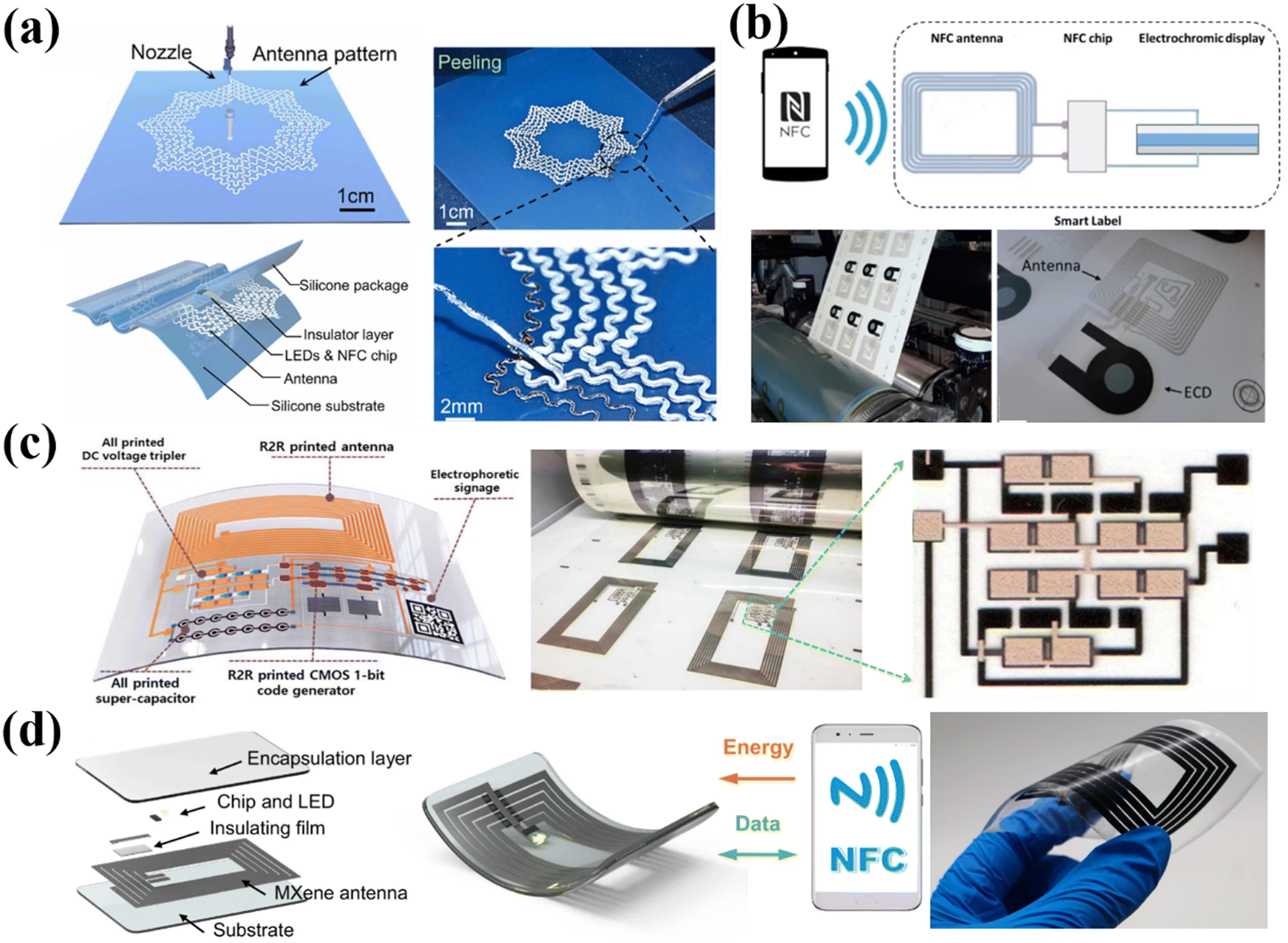 | ||
| Fig. 7 Printable fabrication of antennas on flexible substrates. (a) Stretchable NFC antenna with a spider-web serpentine structure based on the 3D direct-write printing method. Reproduced from ref. 177 with permission from [Elsevier], copyright [2023]. (b) NFC smart labels manufactured via the R2R printing method. Reproduced from ref. 178 with permission from [Springer Nature], copyright [2021]. (c) Fully printed multifunctional label with NFC wireless anti-counterfeiting and item-tracking. Reproduced from ref. 42 with permission from [John Wiley and Sons], copyright [2021]. (d) Fabrication and mechanism of printed MXene NFC tags. Reproduced from ref. 41 with permission from [Springer Nature], copyright [2022]. | ||
6.3. Others
In addition to RFID and NFC antennas, specialized antennas are also designed and employed for specific applications. For instance, in order to simultaneously fulfilling the requirements for near and far field communication, Luadang et al. utilized a planar inverted F antenna (PIFA) structure to integrate a far-field (FF) antenna with an NFC antenna.180 This configuration enables efficient wireless communication in both short-range at 13.56 MHz and long-range communication in the frequency range of 1.8–2.1 GHz. In another work, Rahman et al. presented a wearable ultra-wideband (UWB) antenna designed primarily for brain stroke detection.181 The antenna was implemented on a paper substrate by inkjet printing of copper nanoparticle inks in the form of a coplanar waveguide. It supports a remarkably wide bandwidth that covers the 2.36–2.4 GHz medical body area network band, the 2.4–2.5 GHz industrial, scientific and medical band, and the 3.1–10.6 GHz UWB and so on. The broad frequency range makes it suitable for various applications in the medical field.Overall, printable antennas allow versatile design form factors to fulfill the requirements of diverse communication scenarios, along with attractive properties such as light weight, low cost and sustainability. Table 3 summarizes some of the typical works on printable antennas according to different printing methods, materials, substrates, operating frequencies and other critical factors.
| Type of antenna | Printing method | Printing material | Substrate | Key factor | Operating frequency | Ref. |
|---|---|---|---|---|---|---|
| RFID | Inkjet printing | Ag | PET | — | — | 182 |
| Spray/dispense/contact printing | Graphene | Textiles | - | 13.56 MHz | 171 | |
| 3D printing | Cu | PLA | — | 865–868 MHz | 183 | |
| NFC | R2R | Ag | Polyimide (PI) | Q = 4.1 | 13.56 MHz | 42 |
| R2R | Ag NP | PI | — | above 15.45 MHz | 184 | |
| R2R | Ag NP | PET/PI | Q = 2.9 | 13.56 MHz | 179 | |
| Screen printing | Graphene | Paper | Q = 0.65 | 13.56 MHz | 185 | |
| Dipole antenna | Blade printing | Graphene | Paper | S11 = −13.79 dB | 2.3–2.5 GHz | 172 |
| UWB antenna | Inkjet printing | Cu NP | Paper | S11 = −10dB | 1.91–34.45 GHz | 186 |
| Multi-frequency RF antenna | Screen printing | Ag NW | PET | S11 < −10 dB | 0.71–1.25 and 1.73–2.16 GHz | 174 |
| Far-field/NFC | Screen printing | Ag | PET | S11 < −6 dB | 13.56 MHz | 180 |
7. Printable integrated system for wireless healthcare applications
To realize wireless healthcare applications, it is necessary to associate sensors with wireless transmission circuits into a fully integrated printable sensor system so as to facilitate convenient health status tracking.187 Typically, health monitoring can be categorized into mainly two types: noninvasive and invasive/implantable. This section will focus on printable strategies to realize the integration of multi-functional modules into flexible and miniaturized platforms with robustness.7.1. Noninvasive sensing systems
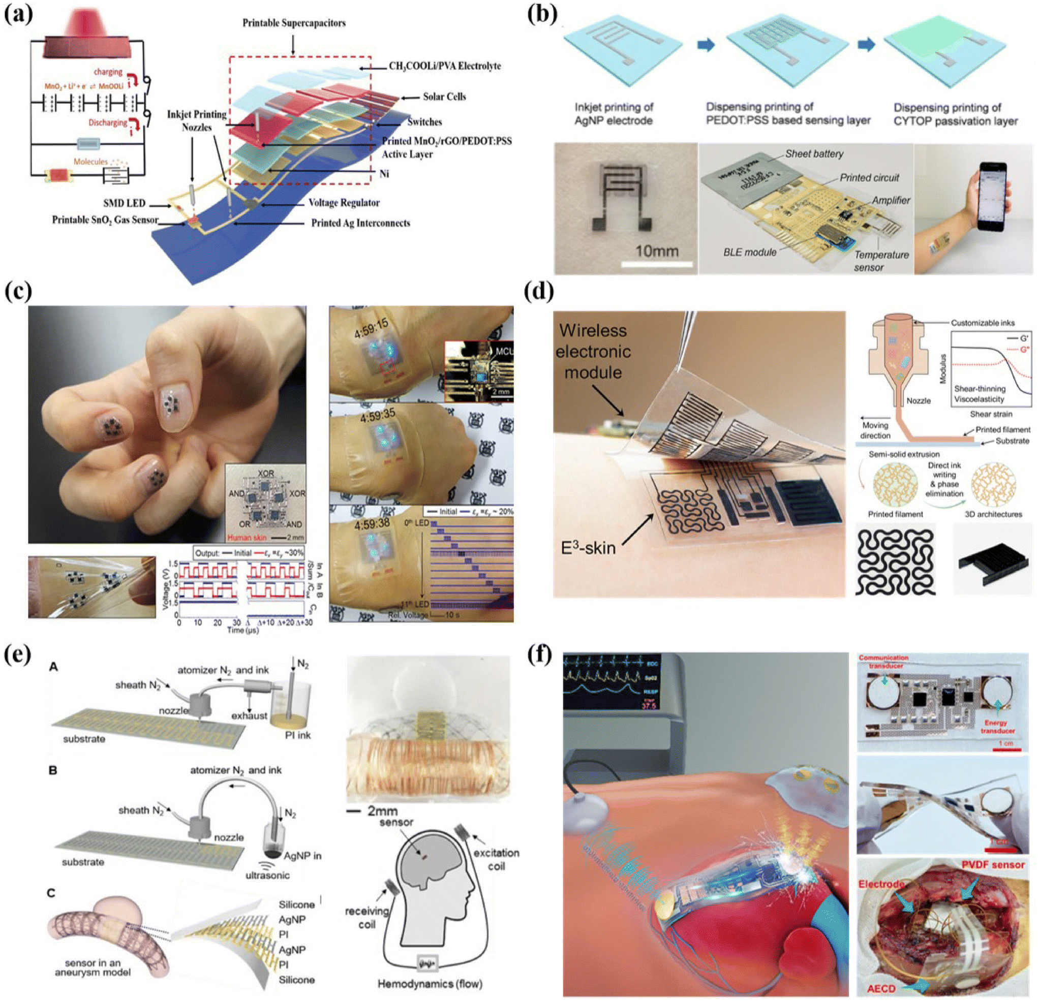 | ||
| Fig. 8 Printable fabrication of integrated and wireless sensing systems for healthcare applications. (a) Schematic illustrations of the fully printable and monolithically integrated smart sensor system. Reproduced from ref. 188 with permission from [John Wiley and Sons], copyright [2018]. (b) A wireless real-time temperature sensing platform. Reproduced from ref. 153 with permission from [Springer Nature], copyright [2020]. (c) Printable and stretchable customized platform for wrist movement sensing. Reproduced from ref. 191 with permission from [Springer Nature], copyright [2017]. (d) 3D printed epifluidic elastic electronic skin (E3) for wireless physiological monitoring. Reproduced from ref. 192 with permission from [American Association for the Advancement of Science], copyright [2023]. (e) Fully printed implantable hemodynamics monitoring biosystems. Reproduced from ref. 194 with permission from [John Wiley and Sons], copyright [2019]. (f) Schematic illustration and images of implantable sensing systems based on ultrasonic energy transfer and communication. Reproduced from ref. 195 with permission from [American Association for the Advancement of Science], copyright [2021]. | ||
Overall, since the device architectures for individual gas sensors are relatively simple, it is quite straightforward to realize sensors by layer-by-layer printing. Since most of the targeted gas analytes for healthcare are at low concentrations, gas sensors based on printed dense films might generate relatively small output signals and could be interfered with humidity and other chemicals. Therefore, hardware designs play a significant role in achieving accurate signal decoding.
Attractively, stretchable and elastic electronic skin can also be implemented in printable approaches. As illustrated in Fig. 8c, Byun et al. developed a fully printed, strain-engineered electronic platform that allows customized multi-functional device integration. To realize stretchable interconnects, the key innovation lies in the structural optimization of the inkjet printed PMMA islands that were enclosed with the PDMS matrix. It also allows enhanced skin-conformability for wearable demonstrations including wrist movement sensing, self-computable digital logics and display.191 Y. Song et al. reported a 3D direct printing technique to fabricate an epifluidic elastic electronic skin (e3-skin) system with multimodal physicochemical sensing capabilities (Fig. 8d).192 This fully printable system consists of a series of electrochemical sweat biosensors and biophysical sensors, a microfluidic system for efficient sweat sampling, and a micro-supercapacitor (MSC) that were further integrated with wireless electronic modules. The custom-designed extrudable inks based on a variety of polymers and nanomaterials, such as Mxenes, play a critical role in efficient maskless 3D printing fabrication and the desirable mechanical robustness of the integrated systems.
7.2. Implantable sensing systems
Compared to noninvasive sensor systems, implantable devices can monitor the internal human environment with in-depth health information, while it poses high requirements on device miniaturization, seamlessly interfacing with tissues, materials biocompatibility and systematic design for reliable wireless communication.193 Therefore, most of the implantable devices and systems are fabricated with traditional microelectronic fabrication techniques, such as the complementary metal–oxide–semiconductor (CMOS) process. The advance in printable devices for such implantable sensing applications is in an early stage and requires further research efforts.For cardiovascular disease diagnosis and monitoring, measuring the hemodynamic parameters such as pressure, flow rate and flow resistance is of great significance. In this regard, Herbert et al. presented a stretchable implantable biosystem for cerebral aneurysm hemodynamics monitoring.194 As shown in Fig. 8e, stretchable capacitor sensors were prepared by aerosol jet printing and can be integrated with stents to be implanted into blood vessels. The system can be operated in a batteryless and wireless manner via inductive coupling of coils. Similarly, they also demonstrated a wireless vascular electronic system with a fully aerosol jet-printed soft sensor to monitor arterial pressure, pulse rate and flow rate. It is highly expected that printed antennas and supporting circuitry can be further explored to be compatibly and seamlessly integrated with such printed sensors, so as to realize fully printable implantable sensing systems with desirable miniaturized sizes and mechanical robustness.
Apart from utilizing antennas for batteryless and wireless sensing, ultrasonic energy transfer and communication technology has emerged as an attractive and convenient strategy for implantable devices in recent years. For instance, Jin et al. developed a soft, adaptable and battery-free implantable system based on flexible transducer arrays (Fig. 8f).195 Casting molds for ultrasonic focusing launchers were prepared by high-resolution 3D printing. Besides, screen printing was adopted to fill solder paste efficiently for convenient connection between metal interconnects and chip components.
The future developments of printable and wireless integrated systems for implantable applications hold great potential in revolutionizing the healthcare industry. By combining facile and cost-effective printing technologies, personalized and miniaturized devices with lower costs can be achieved to enhance the clinical treatment effectiveness and improve the living quality.196 However, implantable devices would pose strict requirements on printable materials and printing resolution to precisely construct micro/nanostructures.197 Future developments of printable and wireless integrated systems are expected to focus on material engineering with biocompatibility and long-term duration, printing accuracy and scalability, as well as standard criteria and privacy regulation.
To meet the increasing demand for both wearable and implantable healthcare devices, it is essential to create sensors and supporting modules that exhibit specific characteristics, such as miniaturized size, robust integration and encapsulation, without a high manufacturing cost. Additionally, incorporating machine learning can enhance signal processing and recognition accuracy while maintaining signal decoding reliability. However, it still remains quite challenging to achieve fully printable fabrication of integrated electronics for wireless health.
8. Conclusion and outlook
In recent years, significant progress has been made in the field of printable electronics, particularly in the development of printable fabrication strategies for integrated sensing systems with wireless data transmission, catering to the needs of smart healthcare. Various sensors and printable antennas have been prepared for applications in remote health monitoring, human–computer interactions, and environmental monitoring. Some of these sensors exhibit high stability and sensitivity, making them ideal candidates for integration into complete sensor systems.This review provides an overview of printable sensor devices with wireless data transmission, starting with an introduction to commonly adopted printing technologies, inks, and substrates. It then highlights typical printable sensors and antennas, followed by the presentation of representative integrated sensor systems based on printable sensors and wireless circuits.
However, several challenges remain in the fabrication of wireless sensor systems. Firstly, the key performance evaluation factors, including the sensitivity and stability of printable sensors, are still less competitive. They often experience decayed performances under mechanical interference or during long-term usage, mainly due to less robustness in printed thin film sensing layers and interfaces. For chemical sensors, exposure to biological fluids can lead to biological contamination, chemical changes, or irreversible non-specific adsorption on the sensor surface. Secondly, reducing communication delay in wireless transmission systems is another important consideration. The communication delay depends on the specific communication technology employed. Real-time biofeedback systems require minimal communication delay, which necessitates the selection of appropriate antennas and optimization of wireless communication circuits.198 Thirdly, as the size of integrated sensing systems continues to be miniaturized, achieving high-level integration becomes crucial. Integrating sensors with other electronic devices and power supply modules into a single flexible platform is a challenge that needs to be addressed. The monolithic integration strategy would ensure mechanical robustness and operational reliability while minimizing signal noises.
In summary, the advances of printable and flexible integrated sensing systems have attracted research interest from interdisciplinary fields, including materials science, electrical engineering and mechanical engineering. Research efforts are expected to emphasize rational engineering on printable materials, electrode patterns/interconnects structural innovation to tackle the existing challenges. There is no doubt that such integrated sensing electronics that can be manufactured in a printable manner will provide feasible, customized, cost-effective and reliable platforms for wireless healthcare.
Conflicts of interest
The authors declare no conflict of interest.Acknowledgements
This work was supported by the National Natural Science Foundation of China (62201243), the Natural Science Foundation of Guangdong Province (2022A1515011928), the Fundamental and Applied Research Grant of Guangdong Province (2021A1515110627) and the Shenzhen Stable Support Plan Program for Higher Education Institutions Research Program (20220815153728002).References
- Y. Luo, M. R. Abidian, J.-H. Ahn, D. Akinwande, A. M. Andrews, M. Antonietti, Z. Bao, M. Berggren, C. A. Berkey, C. J. Bettinger, J. Chen, P. Chen, W. Cheng, X. Cheng, S.-J. Choi, A. Chortos, C. Dagdeviren, R. H. Dauskardt, C.-A. Di, M. D. Dickey, X. Duan, A. Facchetti, Z. Fan, Y. Fang, J. Feng, X. Feng, H. Gao, W. Gao, X. Gong, C. F. Guo, X. Guo, M. C. Hartel, Z. He, J. S. Ho, Y. Hu, Q. Huang, Y. Huang, F. Huo, M. M. Hussain, A. Javey, U. Jeong, C. Jiang, X. Jiang, J. Kang, D. Karnaushenko, A. Khademhosseini, D.-H. Kim, I.-D. Kim, D. Kireev, L. Kong, C. Lee, N.-E. Lee, P. S. Lee, T.-W. Lee, F. Li, J. Li, C. Liang, C. T. Lim, Y. Lin, D. J. Lipomi, J. Liu, K. Liu, N. Liu, R. Liu, Y. Liu, Y. Liu, Z. Liu, Z. Liu, X. J. Loh, N. Lu, Z. Lv, S. Magdassi, G. G. Malliaras, N. Matsuhisa, A. Nathan, S. Niu, J. Pan, C. Pang, Q. Pei, H. Peng, D. Qi, H. Ren, J. A. Rogers, A. Rowe, O. G. Schmidt, T. Sekitani, D.-G. Seo, G. Shen, X. Sheng, Q. Shi, T. Someya, Y. Song, E. Stavrinidou, M. Su, X. Sun, K. Takei, X.-M. Tao, B. C. K. Tee, A. V.-Y. Thean, T. Q. Trung, C. Wan, H. Wang, J. Wang, M. Wang, S. Wang, T. Wang, Z. L. Wang, P. S. Weiss, H. Wen, S. Xu, T. Xu, H. Yan, X. Yan, H. Yang, L. Yang, S. Yang, L. Yin, C. Yu, G. Yu, J. Yu, S.-H. Yu, X. Yu, E. Zamburg, H. Zhang, X. Zhang, X. Zhang, X. Zhang, Y. Zhang, Y. Zhang, S. Zhao, X. Zhao, Y. Zheng, Y.-Q. Zheng, Z. Zheng, T. Zhou, B. Zhu, M. Zhu, R. Zhu, Y. Zhu, Y. Zhu, G. Zou and X. Chen, ACS Nano, 2023, 17, 5211–5295 CrossRef CAS PubMed.
- Y. Zhou, X. Qiu, Z. A. Wan, Z. Long, S. Poddar, Q. Zhang, Y. Ding, C. L. J. Chan, D. Zhang, K. Zhou, Y. Lin and Z. Fan, Nano Energy, 2022, 100, 107516 CrossRef CAS.
- X. Zeng, R. Peng, Z. Fan and Y. Lin, Mater. Today Energy, 2022, 23, 100900 CrossRef CAS.
- L. Gu, S. Poddar, Y. Lin, Z. Long, D. Zhang, Q. Zhang, L. Shu, X. Qiu, M. Kam, A. Javey and Z. Fan, Nature, 2020, 581, 278–282 CrossRef CAS PubMed.
- J. Zhao, H. Y. Y. Nyein, L. Hou, Y. Lin, M. Bariya, C. H. Ahn, W. Ji, Z. Fan and A. Javey, Adv. Mater., 2021, 33, 2006444 CrossRef CAS PubMed.
- L.-C. Tai, C. H. Ahn, H. Y. Y. Nyein, W. Ji, M. Bariya, Y. Lin, L. Li and A. Jamey, ACS Sens., 2020, 5, 1831–1837 CrossRef CAS PubMed.
- X. Ma, R. Peng, W. Mao, Y. Lin and H. Yu, Electrochem. Sci. Adv., 2023, 3, e2100163 CrossRef CAS.
- Y. Shi, Z. Zhang, Q. Huang, Y. Lin and Z. Zheng, J. Semicond., 2023, 44, 021601 CrossRef.
- W. A. D. M. Jayathilaka, K. Qi, Y. Qin, A. Chinnappan, W. Serrano-Garcia, C. Baskar, H. Wang, J. He, S. Cui, S. W. Thomas and S. Ramakrishna, Adv. Mater., 2019, 31, 1805921 CrossRef PubMed.
- W. S. Lee, S. Jeon and S. J. Oh, Nano Convergence, 2019, 6, 1–13 CrossRef PubMed.
- B. Ramachandran and Y.-C. Liao, Biomicrofluidics, 2022, 16, 0116648 CrossRef PubMed.
- X. Ma, P. Wang, L. Huang, R. Ding, K. Zhou, Y. Shi, F. Chen, Q. Zhuang, Q. Huang, Y. Lin and Z. Zheng, Sci. Adv., 2023, 9, 2763–2763 CrossRef PubMed.
- X. Ma, Z. Jiang and Y. Lin, J. Semicond., 2021, 42, 101602 CrossRef CAS.
- X. Sun, C. Zhao, H. Li, H. Yu, J. Zhang, H. Qiu, J. Liang, J. Wu, M. Su, Y. Shi and L. Pan, Micromachines, 2022, 13, 784 CrossRef PubMed.
- H. Landaluce, L. Arjona, A. Perallos, F. Falcone, I. Angulo and F. Muralter, Sensors, 2020, 20, 2495 CrossRef PubMed.
- S. K. Behera, IEEE Sens. J., 2022, 22, 1105–1120 CAS.
- Z. Cao, P. Chen, Z. Ma, S. Li, X. Gao, R.-X. Wu, L. Pan and Y. Shi, Sensors, 2019, 19, 3947 CrossRef CAS PubMed.
- Y. Sun, N. Liu, Z. Yu and Y. Zhou, Chin. J. Sci. Instrum., 2020, 41, 122–137 Search PubMed.
- S. Figueroa Lorenzo, J. Anorga Benito, P. Garcia Cardarelli, J. Alberdi Garaia and S. Arrizabalaga Juaristi, Technologies, 2019, 7, 15 CrossRef.
- P. Swetha, U. Balijapalli and S.-P. Feng, Electrochem. Commun., 2022, 140, 107314 CrossRef CAS.
- Y. Yang, X. Guo, M. Zhu, Z. Sun, Z. Zhang, T. He and C. Lee, Adv. Energy Mater., 2023, 13, 2203040 CrossRef CAS.
- Q. Shi, B. Dong, T. He, Z. Sun, J. Zhu, Z. Zhang and C. Lee, InfoMat, 2020, 2, 1131–1162 CrossRef.
- S. Faham, A. Salimi and R. Ghavami, Talanta, 2023, 253, 123892 CrossRef CAS.
- Z. Song, W. Ye, Z. Chen, Z. Chen, M. Li, W. Tang, C. Wang, Z. A. Wan, S. Poddar, X. Wen, X. Pan, Y. Lin, Q. Zhou and Z. Fan, ACS Nano, 2021, 15, 7659–7667 CrossRef CAS PubMed.
- J. Zhao, Y. Lin, J. Wu, H. Y. Y. Nyein, M. Bariya, L.-C. Tai, M. Chao, W. Ji, G. Zhang, Z. Fan and A. Javey, ACS Sens., 2019, 4, 1925–1933 CrossRef CAS PubMed.
- J. R. Camargo, L. O. Orzari, D. A. G. Araujo, P. R. de Oliveira, C. Kalinke, D. P. Rocha, A. L. dos Santos, R. M. Takeuchi, R. A. A. Munoz, J. A. Bonacin and B. C. Janegitz, Microchem. J., 2021, 164, 105998 CrossRef CAS.
- X. Du, S. P. Wankhede, S. Prasad, A. Shehri, J. Morse and N. Lakal, J. Mater. Chem. C, 2022, 10, 14091–14115 RSC.
- L. Liu, H. Huang, X. Wang, P. He and J. Yang, J. Phys. D: Appl. Phys., 2022, 55, 283002 CrossRef CAS.
- D. Maddipatla, B. B. Narakathu and M. Atashbar, Biosensors, 2020, 10, 10120199 CrossRef PubMed.
- P. Yanez-Sedeno, S. Campuzano and J. M. Pingarron, Biosensors, 2020, 10, 10070076 CrossRef PubMed.
- B. Wang, M. Gao, X. Fu, M. Geng, Y. Liu, N. Cheng, J. Li, L. Li, Z. Zhang and Y. Song, Nano Energy, 2023, 107, 108135 CrossRef CAS.
- C. Zhang, L. Zhang, Z. Pu, B. Bao, W. Ouyang and D. Li, Nano Energy, 2023, 113, 108574 CrossRef CAS.
- S. Zhang, S. M. S. Rana, T. Bhatta, G. B. Pradhan, S. Sharma, H. Song, S. Jeong and J. Y. Park, Nano Energy, 2023, 106, 108110 CrossRef CAS.
- Y. Lin, Y. Gao, F. Fang and Z. Fan, Nano Res., 2018, 11, 3065–3087 CrossRef CAS.
- M. Sun, J. Lv, H. Xu, L. Zhang, Y. Zhong, Z. Chen, X. Sui, B. Wang, X. Feng and Z. Mao, Cellulose, 2020, 27, 2939–2952 CrossRef CAS.
- M. Bariya, Z. Shahpar, H. Park, J. Sun, Y. Jung, W. Gao, H. Y. Y. Nyein, T. S. Liaw, L.-C. Tai, Q. P. Ngo, M. Chao, Y. Zhao, M. Hettick, G. Cho and A. Javey, ACS Nano, 2018, 12, 6978–6987 CrossRef CAS PubMed.
- Y. Sui, Y. Dai, C. C. Liu, R. M. Sankaran and C. A. Zorman, Adv. Mater. Technol., 2019, 4, 1900119 CrossRef CAS.
- H. Lei, K. Cao, Y. Chen, Z. Liang, Z. Wen, L. Jiang and X. Sun, Chem. Eng. J., 2022, 445, 136821 CrossRef CAS.
- B. Zhu, Y. Ling, L. W. Yap, M. Yang, F. Lin, S. Gong, Y. Wang, T. An, Y. Zhao and W. Cheng, ACS Appl. Mater. Interfaces, 2019, 11, 29014–29021 CrossRef CAS PubMed.
- R. K. Mishra, J. R. Sempionatto, Z. Li, C. Brown, N. M. Galdino, R. Shah, S. Liu, L. J. Hubble, K. Bagot, S. Tapert and J. Wang, Talanta, 2020, 211, 120757 CrossRef CAS.
- Y. Shao, L. Wei, X. Wu, C. Jiang, Y. Yao, B. Peng, H. Chen, J. Huangfu, Y. Ying, C. J. Zhang and J. Ping, Nat. Commun., 2022, 13, 3223 CrossRef PubMed.
- J. Sun, S. Parajuli, K. Shrestha, J. Park, S. Shrestha, Y. Jung, H. Park, G. R. Koirala, N. Nasir, S. Kim, H. Truong, H. Jang, J. Lee, J. Lee and G. Cho, Adv. Mater. Technol., 2022, 7, 2100969 CrossRef CAS.
- K. Mondal and M. D. McMurtrey, Mater. Today Chem., 2020, 17, 100328 CrossRef CAS.
- Q. Liu, B. Tian, J. Liang and W. Wu, Mater. Horiz., 2021, 8, 1634–1656 RSC.
- A. M. Tiara, H. Moon, G. Cho and J. Lee, Jpn. J. Appl. Phys., 2022, 61, 0802 Search PubMed.
- R. Abbel, Y. Galagan and P. Groen, Adv. Eng. Mater., 2018, 20, 1701190 CrossRef.
- Y. Choi, Y. Jung, R. Song, J. Park, S. Parajuli, S. Shrestha, G. Cho and B.-S. Kim, Nanomaterials, 2023, 13, 590 CrossRef CAS PubMed.
- J. Lemarchand, N. Bridonneau, N. Battaglini, F. Carn, G. Mattana, B. Piro, S. Zrig and V. Noel, Angew. Chem., Int. Ed., 2022, 61, 202200166 CrossRef PubMed.
- X. Shi, Z.-S. Wu and X. Bao, Electrochem. Energy Rev., 2020, 3, 581–612 CrossRef CAS.
- J. Liang, C. Jiang and W. Wu, Appl. Phys. Rev., 2021, 8, 021319 CAS.
- W. Wu, Nanoscale, 2017, 9, 7342–7372 RSC.
- S. P. Sreenilayam, I. Ul Ahad, V. Nicolosi, V. A. Garzon and D. Brabazon, Mater. Today, 2020, 32, 147–177 CrossRef.
- B. Philip, E. Jewell, P. Greenwood and C. Weirman, J. Manuf. Processes, 2016, 22, 185–191 CrossRef.
- A. Gusain, A. Thankappan and S. Thomas, J. Mater. Sci., 2020, 55, 13490–13542 CrossRef CAS.
- H. W. Choi, T. Zhou, M. Singh and G. E. Jabbour, Nanoscale, 2015, 7, 3338–3355 RSC.
- X. Zhang, K. Liu, V. Sunappan and X. Shan, J. Mater. Process. Technol., 2015, 225, 337–346 CrossRef CAS.
- Z. W. Zhong, J. H. Ee, S. H. Chen and X. C. Shan, Mater. Manuf. Processes, 2020, 35, 564–571 CrossRef CAS.
- S. H. Lee and S. Lee, Int. J. Precis. Eng. Manuf. – Green Technol., 2022, 9, 409–420 CrossRef.
- H. Y. Y. Nyein, M. Bariya, L. Kivimaki, S. Uusitalo, T. S. Liaw, E. Jansson, C. H. Ahn, J. A. Hangasky, J. Zhao, Y. Lin, T. Happonen, M. Chao, C. Liedert, Y. Zhao, L.-C. Tai, J. Hiltunen and A. Javey, Sci. Adv., 2019, 5, 9906 CrossRef PubMed.
- H. Abdolmaleki, P. Kidmose and S. Agarwala, Adv. Mater., 2021, 33, 2006792 CrossRef CAS PubMed.
- N. C. Raut and K. Al-Shamery, J. Mater. Chem. C, 2018, 6, 1618–1641 RSC.
- J. Li, F. Rossignol and J. Macdonald, Lab Chip, 2015, 15, 2538–2558 RSC.
- A. Al-Halhouli, H. Qitouqa, A. Alashqar and J. Abu-Khalaf, Sens. Rev., 2018, 38, 438–452 CrossRef.
- T.-T. Huang and W. Wu, J. Mater. Chem. A, 2019, 7, 23280–23300 RSC.
- B. Derby, in Annual Review of Materials Research, ed. D. R. Clarke, M. Ruhle and F. Zok, 2010, vol. 40, pp. 395–414 Search PubMed.
- X. Li, B. Liu, B. Pei, J. Chen, D. Zhou, J. Peng, X. Zhang, W. Jia and T. Xu, Chem. Rev., 2020, 120, 10596–10636 Search PubMed.
- K. K. B. Hon, L. Li and I. M. Hutchings, CIRP Ann. – Manuf. Technol., 2008, 57, 601–620 CrossRef.
- P. Yang and H. J. Fan, Adv. Mater. Technol., 2020, 5, 2000217 CrossRef CAS.
- E. Tekin, P. J. Smith and U. S. Schubert, Soft Matter, 2008, 4, 703–713 RSC.
- N. Reis, C. Ainsley and B. Derby, J. Appl. Phys., 2005, 97, 094903 CrossRef.
- L. Liu, D. Xiang, Y. Wu, Z. Zhou, H. Li, C. Zhao and Y. Li, Front. Mater., 2021, 8, 725420 CrossRef.
- M. A. Ali, C. Hu, E. A. Yttri and R. Panat, Adv. Funct. Mater., 2022, 32, 2107671 CrossRef CAS PubMed.
- M. Schouten, G. Wolterink, A. Dijkshoorn, D. Kosmas, S. Stramigioli and G. Krijnen, IEEE Sens. J., 2021, 21, 12900–12912 CAS.
- H. Choudhary, D. Vaithiyanathan and H. Kumar, MAPAN, 2021, 36, 405–422 CrossRef.
- J. T. Reeder, Y. Xue, D. Franklin, Y. Deng, J. Choi, O. Prado, R. Kim, C. Liu, J. Hanson, J. Ciraldo, A. J. Bandodkar, S. Krishnan, A. Johnson, E. Patnaude, R. Avila, Y. Huang and J. A. Rogers, Nat. Commun., 2019, 10, 5513 CrossRef CAS PubMed.
- G. L. Goh, H. Zhang, T. H. Chong and W. Y. Yeong, Adv. Electron. Mater., 2021, 7, 2100445 CrossRef CAS.
- M. Ntagios, H. Nassar, A. Pullanchiyodan, W. T. Navaraj and R. Dahiya, Adv. Intell. Syst., 2020, 2, 1900080 CrossRef.
- Z. Pei, Q. Zhang, K. Yang, Z. Yuan, W. Zhang and S. Sang, Adv. Mater. Technol., 2021, 6, 2100038 CrossRef.
- Z. Tang, S. Jia, C. Zhou and B. Li, ACS Appl. Mater. Interfaces, 2020, 12, 28669–28680 CrossRef CAS PubMed.
- T. Kim, Q. Yi, E. Hoang and R. Esfandyarpour, Adv. Mater. Technol., 2021, 6, 2001021 CrossRef CAS.
- Z. Zhu, H. S. Park and M. C. McAlpine, Sci. Adv., 2020, 6, 5575 CrossRef PubMed.
- T. Tuan Sang, N. K. Dutta and N. R. Choudhury, Adv. Colloid Interface Sci., 2018, 261, 41–61 CrossRef PubMed.
- Y. H. Wang, D. X. Du, H. Xie, X. B. Zhang, K. W. Lin, K. Wang and E. Fu, J. Mater. Sci.: Mater. Electron., 2021, 32, 496–508 CrossRef CAS.
- Z. Chu, J. Peng and W. Jin, Sens. Actuators, B, 2017, 243, 919–926 CrossRef CAS.
- K. Rajan, I. Roppolo, A. Chiappone, S. Bocchini, D. Perrone and A. Chiolerio, Nanotechnol., Sci. Appl., 2016, 9, 1–13 CAS.
- S. Xu and W. Wu, Adv. Intell. Syst., 2020, 2, 2000117 CrossRef.
- D. Li, W.-Y. Lai, Y.-Z. Zhang and W. Huang, Adv. Mater., 2018, 30, 1704738 CrossRef PubMed.
- C. S. Boland, U. Khan, H. Benameur and J. N. Coleman, Nanoscale, 2017, 9, 18507–18515 RSC.
- X. Xu, G. Han, H. Yu, X. Jin, J. Yang, J. Lin and C. Ma, J. Phys. D: Appl. Phys., 2020, 53, 05lt02 CrossRef CAS.
- B. Tian, W. Yao, P. Zeng, X. Li, H. Wang, L. Liu, Y. Feng, C. Luo and W. Wu, J. Mater. Chem. C, 2019, 7, 809–818 RSC.
- W. J. Hyun, S. Lim, B. Y. Ahn, J. A. Lewis, C. D. Frisbie and L. F. Francis, ACS Appl. Mater. Interfaces, 2015, 7, 12619–12624 CrossRef CAS PubMed.
- H.-G. Im, S.-H. Jung, J. Jin, D. Lee, J. Lee, D. Lee, J.-Y. Lee, I.-D. Kim and B.-S. Bae, ACS Nano, 2014, 8, 10973–10979 CrossRef CAS PubMed.
- J.-G. Lee, J.-H. Lee, S. An, D.-Y. Kim, T.-G. Kim, S. S. Al-Deyab, A. L. Yarin and S. S. Yoon, J. Mater. Chem. A, 2017, 5, 6677–6685 RSC.
- H.-S. Kim, Y. S. Seo, K. Kim, J. W. Han, Y. Park and S. Cho, Nanoscale Res. Lett., 2016, 11, 230 CrossRef PubMed.
- N. P. Bacalzo Jr., L. P. Go, C. J. Querebillo, P. Hildebrandt, F. T. Limpoco and E. P. Enriquez, ACS Appl. Nano Mater., 2018, 1, 1247–1256 CrossRef.
- P. Pienpinijtham, C. Thammacharoen and S. Ekgasit, Macromol. Res., 2012, 20, 1281–1288 CrossRef CAS.
- J. Rodriguez-Fernandez, J. Perez-Juste, F. Javier Garcia de Abajo and L. M. Liz-Marzan, Langmuir, 2006, 22, 7007–7010 CrossRef CAS PubMed.
- H. He, R. Chen, L. Zhang, T. Williams, X. Fang and W. Shen, J. Colloid Interface Sci., 2020, 562, 333–341 CrossRef CAS PubMed.
- N. A. Luechinger, E. K. Athanassiou and W. J. Stark, Nanotechnology, 2008, 19, 445201 CrossRef PubMed.
- C. Lee, N. R. Kim, J. Koo, Y. J. Lee and H. M. Lee, Nanotechnology, 2015, 26, 455601 CrossRef PubMed.
- X. Yu, J. Li, T. Shi, C. Cheng, G. Liao, J. Fan, T. Li and Z. Tang, J. Alloys Compd., 2017, 724, 365–372 CrossRef CAS.
- E. B. Choi and J.-H. Lee, Appl. Surf. Sci., 2019, 480, 839–845 CrossRef CAS.
- Y. Zhang, P. Zhu, G. Li, Z. Cui, C. Cui, K. Zhang, J. Gao, X. Chen, G. Zhang, R. Sun and C. Wong, ACS Appl. Mater. Interfaces, 2019, 11, 8382–8390 CrossRef CAS PubMed.
- T. G. Kim, H. J. Park, K. Woo, S. Jeong, Y. Choi and S. Y. Lee, ACS Appl. Mater. Interfaces, 2018, 10, 1059–1066 CrossRef CAS PubMed.
- M. Grouchko, A. Kamyshny and S. Magdassi, J. Mater. Chem., 2009, 19, 3057–3062 RSC.
- J. Perelaer, B.-J. de Gans and U. S. Schubert, Adv. Mater., 2006, 18, 2101 CrossRef CAS.
- H. Jiang, L. Zheng, Z. Liu and X. Wang, InfoMat, 2020, 2, 1077–1094 CrossRef CAS.
- G. Hu, J. Kang, L. W. T. Ng, X. Zhu, R. C. T. Howe, C. G. Jones, M. C. Hersam and T. Hasan, Chem. Soc. Rev., 2018, 47, 3265–3300 RSC.
- K. Pan, Y. Fan, T. Leng, J. Li, Z. Xin, J. Zhang, L. Hao, J. Gallop, K. S. Novoselov and Z. Hu, Nat. Commun., 2018, 9, 5197 CrossRef PubMed.
- A. S. Pavlova, E. A. Obraztsova, A. V. Belkin, C. Monat, P. Rojo-Romeo and E. D. Obraztsova, J. Nanophotonics, 2016, 10, 012525 CrossRef.
- V. Nicolosi, M. Chhowalla, M. G. Kanatzidis, M. S. Strano and J. N. Coleman, Science, 2013, 340, 1420 CrossRef CAS.
- M. Yi and Z. Shen, J. Mater. Chem. A, 2015, 3, 11700–11715 RSC.
- M. Lotya, P. J. King, U. Khan, S. De and J. N. Coleman, ACS Nano, 2010, 4, 3155–3162 CrossRef CAS PubMed.
- T. S. Tran, S. J. Park, S. S. Yoo, T.-R. Lee and T. Kim, RSC Adv., 2016, 6, 12003–12008 RSC.
- D. S. Kim, J.-M. Jeong, H. J. Park, Y. K. Kim, K. G. Lee and B. G. Choi, Nano-Micro Lett., 2021, 13, 87 CrossRef CAS PubMed.
- K. Parvez, R. Worsley, A. Alieva, A. Felten and C. Casiraghi, Carbon, 2019, 149, 213–221 CrossRef CAS.
- X. Liang, H. Li, J. Dou, Q. Wang, W. He, C. Wang, D. Li, J.-M. Lin and Y. Zhang, Adv. Mater., 2020, 32, 2000165 CrossRef CAS PubMed.
- J. O. Akindoyo, N. H. Ismail and M. Mariatti, J. Mater. Sci.: Mater. Electron., 2021, 32, 12648–12660 CrossRef CAS.
- J. Sun, R. Sun, P. Jia, M. Ma and Y. Song, J. Mater. Chem. C, 2022, 10, 9441–9464 RSC.
- T. Vinh Van, S. Lee, D. Lee and L. Thanh-Hai, Polymers, 2022, 14, 3730 CrossRef PubMed.
- S. Zhang, Y. Chen, H. Liu, Z. Wang, H. Ling, C. Wang, J. Ni, B. C. Saltik, X. Wang, X. Meng, H.-J. Kim, A. Baidya, S. Ahadian, N. Ashammakhi, M. R. Dokmeci, J. Travas-Sejdic and A. Khademhosseini, Adv. Mater., 2020, 32, 1904752 CrossRef CAS PubMed.
- V. R. Feig, H. Tran, M. Lee and Z. Bao, Nat. Commun., 2018, 9, 2740 CrossRef PubMed.
- J. Rivnay, S. Inal, B. A. Collins, M. Sessolo, E. Stavrinidou, X. Strakosas, C. Tassone, D. M. Delongchamp and G. G. Malliaras, Nat. Commun., 2016, 7, 11287 CrossRef PubMed.
- A. Corletto and J. G. Shapter, J. Mater. Chem. C, 2021, 9, 14161–14174 RSC.
- T. Ren, H. Yang, J. Zhang, K. Lv, D. Kong, F. Jiang, Y. Chang, P. Yu, J. Tao, D. Wang, N. Kong and Y. Shao, Adv. Eng. Mater., 2023, 25, 2301018 CrossRef CAS.
- R. Luo, X. Li, H. Li, B. Du and S. Zhou, Prog. Org. Coat., 2022, 162, 106593 CrossRef CAS.
- L.-W. Lo, J. Zhao, H. Wan, Y. Wang, S. Chakrabartty and C. Wang, ACS Appl. Mater. Interfaces, 2021, 13, 21693–21702 CrossRef CAS PubMed.
- M. Prosa, M. Tessarolo, M. Bolognesi, T. Cramer, Z. Chen, A. Facchetti, B. Fraboni, M. Seri, G. Ruani and M. Muccini, Adv. Mater. Interfaces, 2016, 3, 1600770 CrossRef.
- U. Kraft, F. Molina-Lopez, D. Son, Z. Bao and B. Murmann, Adv. Electron. Mater., 2020, 6, 1900681 CrossRef CAS.
- D. D. C. Rasi, P. M. J. G. van Thiel, H. Bin, K. H. Hendriks, G. H. L. Heintges, M. M. Wienk, T. Becker, Y. Li, T. Riedl and R. A. J. Janssen, Sol. RRL, 2019, 3, 1800366 CrossRef.
- E. K. Arora, V. Sharma, A. Ravi, A. Shahi, S. Jagtap, A. Adhikari, J. K. Dash, P. Kumar and R. Patel, Energies, 2023, 16, 6716 CrossRef CAS.
- S. Choudhury, D. Deepak, G. Bhattacharya, J. McLaughlign and S. S. Roy, Macromol. Mater. Eng., 2023, 2300007 CrossRef CAS.
- K. A. Saraswathi, M. S. B. Reddy, N. Jayarambabu, S. Aich and T. V. Rao, Mater. Lett., 2023, 349, 134850 CrossRef CAS.
- Y. Zhao, Y. Yu, S. Zhao, R. Zhu, J. Zhao and G. Cui, Microchem. J., 2023, 185, 108092 CrossRef CAS.
- C. Zhu, H. Xue, H. Zhao, T. Fei, S. Liu, Q. Chen, B. Gao and T. Zhang, Talanta, 2022, 242, 123289 CrossRef CAS PubMed.
- E. Bilbao, S. Kapadia, V. Riechert, J. Amalvy, F. N. Molinari, M. M. Escobar, R. R. Baumann and L. N. Monsalve, Sens. Actuators, B, 2021, 346, 130558 CrossRef CAS.
- M. Zea, R. Texido, R. Villa, S. Borros and G. Gabriel, ACS Appl. Mater. Interfaces, 2021, 13, 33524–33535 CrossRef CAS PubMed.
- H. Ervasti, T. Jarvinen, O. Pitkanen, E. Bozo, J. Hiitola-Keinanen, O.-H. Huttunen, J. Hiltunen and K. Kordas, ACS Appl. Mater. Interfaces, 2021, 13, 27284–27294 CrossRef CAS PubMed.
- A. Khan, K. Rahman, S. Ali, S. Khan, R. Wang and A. Bermak, J. Mater. Res., 2021, 36, 3568–3578 CrossRef CAS.
- M. T. Rahman, C.-Y. Chen, B. Karagoz, M. Renn, M. Schrandt, A. Gellman and R. Panat, ACS Appl. Nano Mater., 2019, 2, 3280–3291 CrossRef CAS.
- S. Agarwala, G. L. Goh, L. Truong-Son Dinh, J. An, Z. K. Peh, W. Y. Yeong and Y.-J. Kim, ACS Sens., 2019, 4, 218–226 CrossRef CAS PubMed.
- J. Wang, C. Lu and K. Zhang, Energy Environ. Mater., 2020, 3, 80–100 CrossRef.
- R. Cao, X. Pu, X. Du, W. Yang, J. Wang, H. Guo, S. Zhao, Z. Yuan, C. Zhang, C. Li and Z. L. Wang, ACS Nano, 2018, 12, 5190–5196 CrossRef CAS PubMed.
- J.-W. Lee, Y. Choi, J. Jang, S.-H. Yeom, W. Lee and B.-K. Ju, Sens. Actuators, A, 2020, 313, 112205 CrossRef CAS.
- D. Barmpakos, C. Tsamis and G. Kaltsas, Microelectron. Eng., 2020, 225, 111266 CrossRef CAS.
- Z. Deng, T. Hu, Q. Lei, J. He, P. X. Ma and B. Guo, ACS Appl. Mater. Interfaces, 2019, 11, 6796–6808 CrossRef CAS PubMed.
- X.-Y. Yin, Y. Zhang, X. Cai, Q. Guo, J. Yang and Z. L. Wang, Mater. Horiz., 2019, 6, 767–780 RSC.
- J. Gao, Y. Fan, Q. Zhang, L. Luo, X. Hu, Y. Li, J. Song, H. Jiang, X. Gao, L. Zheng, W. Zhao, Z. Wang, W. Ai, Y. Wei, Q. Lu, M. Xu, Y. Wang, W. Song, X. Wang and W. Huang, Adv. Mater., 2022, 34, 2107511 CrossRef CAS PubMed.
- Y. Li, Y. Wei, Y. Yang, L. Zheng, L. Luo, J. Gao, H. Jiang, J. Song, M. Xu, X. Wang and W. Huang, Research, 2022, 2022, 0002 CrossRef CAS.
- J. Sato, T. Sekine, W. Yi-Fei, Y. Takeda, H. Matsui, D. Kumaki, F. D. Dos Santos, A. Miyabo and S. Tokito, Sens. Actuators, A, 2019, 295, 93–98 CrossRef CAS.
- Y. Yang, H. Wang, Y. Hou, S. Nan, Y. Di, Y. Dai, F. Li and J. Zhang, Compos. Sci. Technol., 2022, 226, 109518 CrossRef CAS.
- W. Li, M. Xu, J. Gao, X. Zhang, H. Huang, R. Zhao, X. Zhu, Y. Yang, L. Luo, M. Chen, H. Ji, L. Zheng, X. Wang and W. Huang, Adv. Mater., 2023, 35, 2207447 CrossRef CAS PubMed.
- Y.-F. Wang, T. Sekine, Y. Takeda, K. Yokosawa, H. Matsui, D. Kumaki, T. Shiba, T. Nishikawa and S. Tokito, Sci. Rep., 2020, 10, 2467 CrossRef CAS PubMed.
- Y. Lin, M. Bariya, H. Y. Y. Nyein, L. Kivimaki, S. Uusitalo, E. Jonsson, W. Ji, Z. Yuan, T. Happonen, C. Liedert, J. Hiltunen, Z. Fan and A. Javey, Adv. Funct. Mater., 2019, 29, 1902521 CrossRef.
- K. Nagamine, T. Mano, A. Nomura, Y. Ichimura, R. Izawa, H. Furusawa, H. Matsui, D. Kumaki and S. Tokito, Sci. Rep., 2019, 9, 1–8 CrossRef CAS PubMed.
- S. A. Goodchild, L. J. Hubble, R. K. Mishra, Z. Li, K. Y. Goud, A. Barfidokht, R. Shah, K. S. Bagot, A. J. S. McIntosh and J. Wang, Anal. Chem., 2019, 91, 3747–3753 CrossRef CAS PubMed.
- R. Jin, D. Kong, X. Zhao, H. Li, X. Yan, F. Liu, P. Sun, D. Du, Y. Lin and G. Lu, Biosens. Bioelectron., 2019, 141, 111473 CrossRef CAS PubMed.
- J. Liu, X. Jiang, R. Zhang, Y. Zhang, L. Wu, W. Lu, J. Li, Y. Li and H. Zhang, Adv. Funct. Mater., 2019, 29, 1807326 CrossRef.
- D. Lv, W. Chen, W. Shen, M. Peng, X. Zhang, R. Wang, L. Xu, W. Xu, W. Song and R. Tan, Sens. Actuators, B, 2019, 298, 126890 CrossRef CAS.
- G. Manjunath, P. Nagaraju and S. Mandal, J. Mater. Sci.: Mater. Electron., 2021, 32, 5713–5728 CrossRef CAS.
- C. Li, J. Xiong, C. Zheng and J. Zhao, ACS Appl. Nano Mater., 2022, 5, 16655–16663 CrossRef CAS.
- S. Tajik, H. Beitollahi, S. A. Ahmadi, M. B. Askari and A. Di Bartolomeo, Nanomaterials, 2021, 11, 3208 CrossRef CAS PubMed.
- K. Shrestha, Y. Kim, Y. Jung, S. Kim, H. Truong and G. Cho, Flexible Printed Electron., 2021, 6, 044001 CrossRef CAS.
- C. Liedert, L. Rannaste, A. Kokkonen, O.-H. Huttunen, R. Liedert, J. Hiltunen and L. Hakalahti, ACS Sens., 2020, 5, 2010–2017 CrossRef CAS PubMed.
- Y.-S. Huang, K.-Y. Chen, Y.-T. Cheng, C.-K. Lee and H.-E. Tsai, IEEE Electron Device Lett., 2020, 41, 597–600 CAS.
- L.-W. Lo, H. Shi, H. Wan, Z. Xu, X. Tan and C. Wang, Adv. Mater. Technol., 2020, 5, 1900717 CrossRef CAS.
- P. B. Deroco, D. Wachholz Junior and L. T. Kubota, Chemosensors, 2021, 9, 61 CrossRef CAS.
- S. I. Kim, H. Y. Jung, S. Yang, J. Yoon, H. Lee and W. Ryu, Virtual Phys. Prototyping, 2022, 17, 156–169 CrossRef.
- A. G. G. Samarentsis, G. Makris, S. Spinthaki, G. Christodoulakis, M. Tsiknakis and A. K. K. Pantazis, Sensors, 2022, 22, 9725 CrossRef PubMed.
- J. Kim, G. A. Salvatore, H. Araki, A. M. Chiarelli, Z. Xie, A. Banks, X. Sheng, Y. Liu, J. W. Lee, K.-I. Jang, S. Y. Heo, K. Cho, H. Luo, B. Zimmerman, J. Kim, L. Yan, X. Feng, S. Xu, M. Fabiani, G. Gratton, Y. Huang, U. Paik and J. A. Rogers, Sci. Adv., 2016, 2, 1600418 CrossRef PubMed.
- T. Delipinar, E. A. Ozek, C. E. Kaya, S. Tanyeli and M. K. Yapici and Ieee, 2020 IEEE International Conference on Flexible and Printable Sensors and Systems (FLEPS), 2020, pp. 1–4.
- W. Wang, C. Ma, X. Zhang, J. Shen, N. Hanagata, J. Huangfu and M. Xu, Sci. Technol. Adv. Mater., 2019, 20, 870–875 CrossRef PubMed.
- G. Muntoni, G. Montisci, G. A. Casula, F. P. Chietera, A. Michel, R. Colella, L. Catarinucci and G. Mazzarella, IEEE Antennas Wireless Propag. Lett., 2020, 19, 1118–1122 Search PubMed.
- W. Li, E. Yarali, A. Bakytbekov, T. D. Anthopoulos and A. Shamim, Nanotechnology, 2020, 31, 395201 CrossRef CAS PubMed.
- S. Niu, N. Matsuhisa, L. Beker, J. Li, S. Wang, J. Wang, Y. Jiang, X. Yan, Y. Yun, W. Burnetts, A. S. Y. Poon, J. B. H. Tok, X. Chen and Z. Bao, Nat. Electron., 2019, 2, 361–368 CrossRef.
- L. Lin, M. Dautta, A. Hajiaghajani, A. R. Escobar, P. Tseng and M. Khine, Adv. Electron. Mater., 2021, 7, 2000765 CrossRef CAS.
- Z. He, Y. Wang, H. Xiao, Y. Wu, X. Xia, S. Li, J. Liu, K. Huang, F. Wang, J. Shang, Y. Liu, H. Li, F. Li, S. Wang, G. Zhu and R.-W. Li, Nano Energy, 2023, 112, 108461 CrossRef CAS.
- L. Hakola, E. Jansson, R. Futsch, T. Happonen, V. Thenot, G. Depres, A. Rougier and M. Smolander, Int. J. Adv. Manuf. Technol., 2021, 117, 2921–2934 CrossRef.
- B. B. Maskey, K. Shrestha, J. Sun, H. Park, J. Park, S. Parajuli, S. Shrestha, Y. Jung, S. Ramasundaram, G. R. Koirala and G. Cho, RSC Adv., 2020, 10, 12407–12414 RSC.
- B. Luadang, A. Sakonkanapong, S. Dentri, R. Pansomboon and C. Phongcharoenpanich, IEEE Access, 2019, 7, 171966–171973 Search PubMed.
- M. A. Rahman, M. F. Hossain, M. Hossain and R. Ahmmed, Egypt. Inf. J., 2020, 21, 23–35 Search PubMed.
- G. Ponraj, W. L. Yeo, K. S. Kumar, M. S. Kalairaj, C. J. Cai and H. Ren and IeeeXian, PEOPLES R CHINA, 2021.
- G. Muntoni, G. Montisci, G. A. Casula, F. P. Chietera, A. Michel, R. Colella, L. Catarinucci and G. Mazzarella, IEEE Antennas Wireless Propag. Lett., 2020, 19, 1118–1122 Search PubMed.
- B. B. Maskey, J. Sun, K. Shrestha, S. Kim, M. Park, Y. Kim, H. Park, S. Lee, Y. Han, J. Lee, Y. Majima, J. Kim, J. Lee, G. Bahk, G. R. Koirala and G. Cho, IEEE Sens. J., 2020, 20, 2106–2116 Search PubMed.
- T. Leng, K. Parvez, K. Pan, J. Ali, D. McManus, K. S. Novoselov, C. Casiraghi and Z. Hu, 2D Mater., 2020, 7, 024004 CrossRef CAS.
- M. A. Rahman and M. F. Hossain, 2019 International Conference on Computer, Communication, Chemical, Materials and Electronic Engineering (IC4ME2), 2019, pp. 1–6 Search PubMed.
- Y. Guo, X. Wei, S. Gao, W. Yue, Y. Li and G. Shen, Adv. Funct. Mater., 2021, 31, 2104288 CrossRef CAS.
- Y. Lin, J. Chen, M. M. Tavakoli, Y. Gao, Y. Zhu, D. Zhang, M. Kam, Z. He and Z. Fan, Adv. Mater., 2019, 31, 1804285 CrossRef PubMed.
- R. K. Mishra, A. Martin, T. Nakagawa, A. Barfidokht, X. Lu, J. R. Sempionatto, K. M. Lyu, A. Karajic, M. M. Musameh, I. L. Kyratzis and J. Wang, Biosens. Bioelectron., 2018, 101, 227–234 CrossRef CAS PubMed.
- L. Gillan, T. Teerinen, M. Suhonen, L. Kivimaki and A. Alastalo, Flexible Printed Electron., 2021, 6, 034003 CrossRef CAS.
- J. Byun, B. Lee, E. Oh, H. Kim, S. Kim, S. Lee and Y. Hong, Sci. Rep., 2017, 7, 45328 CrossRef CAS PubMed.
- Y. Song, R. Y. Tay, J. Li, C. Xu, J. Min, E. S. Sani, G. Kim, W. Heng, I. Kim and W. Gao, Sci. Adv., 2023, 9, 6492 CrossRef PubMed.
- R. Herbert, H.-R. Lim, S. Park, J.-H. Kim and W.-H. Yeo, Adv. Healthcare Mater., 2021, 10, 2100158 CrossRef CAS PubMed.
- R. Herbert, S. Mishra, H.-R. Lim, H. Yoo and W.-H. Yeo, Adv. Sci., 2019, 6, 1901034 CrossRef CAS PubMed.
- P. Jin, J. Fu, F. Wang, Y. Zhang, P. Wang, X. Liu, Y. Jiao, H. Li, Y. Chen, Y. Ma and X. Feng, Sci. Adv., 2021, 7, 2507 CrossRef PubMed.
- G. Liu, Z. Lv, S. Batool, M.-Z. Li, P. Zhao, L. Guo, Y. Wang, Y. Zhou and S.-T. Han, Small, 2023, 19, 2207879 CrossRef CAS PubMed.
- T. Lu, S. Ji, W. Jin, Q. Yang, Q. Luo and T.-L. Ren, Sensors, 2023, 23, 2991 CrossRef CAS PubMed.
- A. Kos, V. Milutinovic and A. Umek, Future Gener. Comput. Syst., 2019, 92, 582–592 CrossRef.
Footnote |
| † These authors contributed equally to this work. |
| This journal is © The Royal Society of Chemistry 2024 |