
 Open Access Article
 This Open Access Article is licensed under a Creative Commons Attribution-Non Commercial 3.0 Unported Licence
Single-molecule tip-enhanced Raman spectroscopy of C60 on the Si(111)-(7 × 7) surface†
Borja Cirera‡
 *ab,
Shuyi Liu‡ac,
Youngwook Parka,
Ikutaro Hamadad,
Martin Wolfa,
Akitoshi Shiotaria and
Takashi Kumagaiae
*ab,
Shuyi Liu‡ac,
Youngwook Parka,
Ikutaro Hamadad,
Martin Wolfa,
Akitoshi Shiotaria and
Takashi Kumagaiae
aDepartment of Physical Chemistry, Fritz-Haber Institute of the Max-Planck Society, Faradayweg 4-6, Berlin 14195, Germany. E-mail: borja.cirera@csic.es
bInstituto de Ciencia de Materiales de Madrid (CSIC), Campus de Excelencia de la Universidad Autónoma de Madrid, c/Sor Juana Inés de la Cruz 3, 28049, Spain
cWuhan National Laboratory for Optoelectronics, Huazhong University of Science and Technology, Wuhan, China
dDepartment of Precision Engineering, Graduate School of Engineering, Osaka University, 2-1 Yamadaoka, Suita, Osaka 565-0871, Japan
eCenter for Mesoscopic Sciences, Institute for Molecular Science, Okazaki 444-8585, Japan
First published on 31st July 2024
Abstract
Tip-enhanced Raman spectroscopy (TERS), combined with low-temperature scanning tunnelling microscopy (STM), has emerged as a highly sensitive method for chemical characterization, offering even sub-molecular resolution. However, its exceptional sensitivity is generally limited to molecules adsorbed onto plasmonic surfaces. Here we demonstrate single-molecule TERS for fullerene (C60) adsorbed on the Si(111)-(7 × 7) reconstructed surface. Distinct adsorption geometries of C60 are manifested in the TERS spectra. In addition, we reveal that formation of a molecular-point-contact (MPC) drastically enhances Raman scattering and leads to the emergence of additional vibrational peaks, including overtones and combinations. In the MPC regime, the anti-Stokes peaks are observed, revealing that vibrationally excited states are populated through optical excitation of the MPC junction, whereas showing no significant vibrational heating by current flow via inelastic electron–vibration scattering. Our results will open up the possibility of applying TERS for semiconducting surfaces and studying microscopic mechanisms of vibrational heating in metal–molecule–semiconductor nanojunctions.
Introduction
Understanding the structures and properties of organic molecules on semiconductor surfaces is of fundamental importance for the performance and functionality of organic–inorganic hybrid devices and molecular electronics.1 Scanning probe microscopy (SPM) has been employed to directly study single molecules on various substrates, ranging from metals to insulating thin films and semiconductrors,2,3 and provides unique opportunities to characterize and manipulate the structures and properties of individual molecules.4 The combination of optical techniques with low-temperature SPM has recently led to remarkable advancements5,6 such as highly sensitive single-molecule Raman and photoluminescence (PL) spectroscopy, sub-molecular spectroscopic imaging,7–10 detection of photo-currents,11 control of photo-reactions,12 and observation of ultrafast coherent dynamics.13 However, many of these applications primarily rely on the strong enhancement and confinement of electromagnetic fields occurring in the plasmonic nanogaps,14 restricting its application mostly to plasmonic metal substrates. Among these methods, tip-enhanced Raman spectroscopy (TERS) is the most established, allowing detailed chemical analysis of surface adsorbates. Applying TERS to semiconductor surfaces is a significant challenge to extend its applications and indeed, it has been recently shown that intense TERS signals are obtained on Si surfaces, demonstrating the observation of surface phonons or single molecules.15,16 However, further examples are necessary to elucidate the enhancement mechanism.Here, we demonstrate single-molecule TERS measurements of C60 on the Si(111)-(7 × 7) reconstructed surface with approximately 1-nm resolution. The enhancement factor is quantified by comparing the TERS intensity with the optical phonon mode of the bulk Si. Furthermore, the additional drastic enhancement of the Raman scattering when a molecular-point-contact (MPC) between the tip and a single C60 molecule is formed, enables the observation of the anti-Stokes peaks and investigation of potential vibrational excitations (heating) in the current-carrying metal–molecule–semiconductor junction. This provides microscopic insights into vibrational heating through inelastic electron–phonon coupling.17–19
To investigate single C60 molecules on the Si surface, as schematically depicted in Fig. 1a, we prepare a low coverage sample by depositing the molecules using Knudsen cell with the sample kept at room temperature (see Methods in ESI†). The strong interaction between the C60 and the Si(111)-(7 × 7) reconstructed surface inhibits surface diffusion and the formation of extended self-assembled islands,20–22 resulting in isolated single C60 on the surface and a stable junction under illumination with an irradiance of ∼1 W cm−2 at liquid nitrogen temperatures. Fig. 1b shows a topographic scanning tunnelling microscopy (STM) image of an isolated C60 on the Si(111)-(7 × 7) surface, with the atomic structure of the reconstructed surface resolved. The characteristic (7 × 7) reconstruction of the Si surface consists of two halves:23 the faulted and the unfaulted triangular subunit cells, leading to a variety of different adsorption sites. The high-resolution image allows to distinguish the adsorption site close to the centre of the faulted unit cell, depicted as the grey triangle in Fig. 1b. TERS of a single C60 is obtained with an Ag tip and 532-nm excitation wavelength in the tunnelling regime (Fig. 1c). By comparing the spectra of the C60 (blue curve) with that of the bare Si surface (black), a Raman peak at 520 cm−1 and broad peak below 180 cm−1 can be assigned to the optical phonon mode of the Si bulk and the Ag tip phonon modes, respectively.15,24 Thus, the remaining peaks in the spectrum over C60 are attributed to molecular vibrations. Particularly, the most intense peak at 1441 cm−1 can be assigned to the Ag(2) mode of C60, in agreement with previous experiments on other surfaces.25 The high sensitivity of our setup allows imaging of the spatial distribution of the Ag(2) mode (Fig. 1d), which reveals a potential sub-molecular feature. Other intense adjacent modes at 1382 and 1478 cm−1 can be also mapped with the comparable resolution (see Fig. S1, ESI†). The slight asymmetry observed in the TERS mapping of these vibrational modes may be due to the adsorption geometry of C60 and the orientation of the topmost pentagonal ring.4 These results suggest that the observed Raman scattering occurs through the interaction with the plasmonic field tightly localized at a (sub-)nanostructure, specifically nanotip at the Ag tip apex.26 Although the Si substrate does not support localized surface plasmon resonance (LSPR) in the visible range, the nanotip can provide an extreme field enhancement at very close tip–sample distances,16 resulting in ∼1 nm resolution (Fig. 1d).27
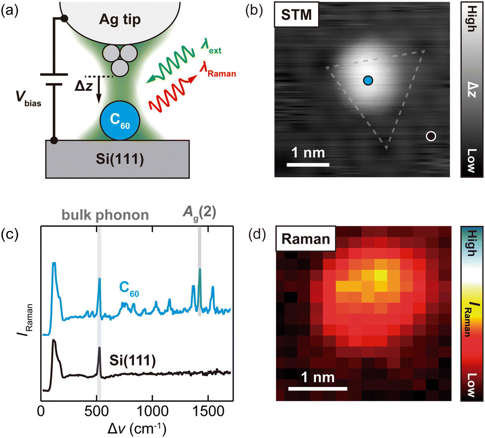 | ||
| Fig. 1 (a) Schematic of the experimental configuration: a single C60 molecule junction is formed in the STM junction consisting of the reconstructed Si(111)-(7 × 7) substrate and an Ag tip. (b) STM image of a single C60 molecule on the Si(111)-(7 × 7) surface, scanned under illumination with the faulted region highlighted with a grey triangle (80 K, Vbias = 0.3 V, jSTM = 60 pA, λext = 532 nm, P = 5 mW). (c) TERS spectra recorded over the individual C60 (blue) and over the bare Si surface (black) acquired on the points depicted in (b) (averaging time = 5 s). (d) TERS map of the Ag(2) peak (80 K, feedback on, setpoint: Vbias = 0.3 V and jSTM = 50 pA, λext = 532 nm, Pext = 5.5 mW, 16 × 14 pixels, 5 s per point, TERS scale bar: arbitrary units). | ||
Surprisingly, the observed TERS intensity for a single C60 is comparable to the far-field Raman scattering intensity of the optical phonon mode of the bulk Si. Based on the Raman cross sections of the bulk phonon and the Ag(2) mode of C60, we estimate the total TERS enhancement factor to be ∼1012 (see Section 3 in ESI†). According to classical simulations of the electric field in an Ag–Si STM junction,16 the field enhancement is calculated to be ∼109 at the expected tip–surface distance in the tunnelling regime. Thus, the observed enhancement cannot be rationalized solely by the electromagnetic enhancement, suggesting a significant contribution from the chemical enhancement, leading to overall enhancement comparable to that on metallic surfaces. The TERS intensity observed in the Ag tip–C60–Si surface is comparable to that in Ag tip–C60–Ag surface.25 This implies that the approximately 2 orders of magnitude lower electric field on the Ag–Si junction compared to the Ag–Ag case is supplied mainly by the chemical enhancement. The larger contribution of chemical enhancement will originate from a stronger molecular–surface interaction between the molecule and Si surface compared to the Ag surface. Previous surface-enhanced Raman spectroscopy experiments have shown that drastic chemical enhancement such as 105 occurs on semiconductors through charge transfer,28 inspiring the exploration of vibrational spectroscopic experiments of C60 on other semiconducting surfaces. We also note that the relative intensity between the C60 and the Si bulk is around 2 orders of magnitude larger than previous results for a double-decker phthalocyanine on the same surface under similar tunnelling tip–sample distance conditions,16 indicating an unexpectedly large enhancement for C60.
We measured TERS of C60 molecules adsorbed on various sites of the Si(111)-(7 × 7) surface, which are reflected in the distinct appearance in STM images. Fig. 2 shows three distinct TERS spectra obtained from three different single molecules along with their corresponding STM images (see Fig. S2 for the spectra without the Si signal, ESI†). Spectra (a) and (b) are from molecules adsorbed on the unfaulted half unit of the Si(111)-(7 × 7) surface, with (b) closer to the corner hole.29 The red spectrum (c) is acquired from a single C60 on the faulted half, in accordance with the molecule in Fig. 1. Notably, each spectrum exhibits characteristic features, including distinct peak positions and relative peak intensities. Furthermore, by comparing the observed peaks with Raman spectra on C60 in the solid state and Ag(111) (refer to Table S1, ESI†), it is clear that the spectra show more peaks than expected from Raman selection rules for icosahedral (Ih) symmetry, which allows 10 active modes. While our STM images do not resolve the detailed molecular orientation relative to the surface, it will affect molecule–surface interactions.29–31 The strong interaction between molecules and the Si(111)-(7 × 7) surface32 has two different effects on the vibrational spectra. First, the splitting of vibrational modes is observed when C60 is adsorbed on surfaces, which is associated with the lifting of degeneracy due to symmetry lowering as C60 is deformed upon adsorption, which depends on the interaction between the molecule and the underlying surface.25 Second, this interaction can also lead to the formation of covalent Si–C bonds, with the subsequent change of the surrounding C–C bonds, which may also be manifested as new peaks in the TERS spectra. The detailed assignments of the observed peaks would be a future challenge in the TERS simulations. Although most of the single C60 molecules exhibit a stable TERS signal over time (refer to Fig. S3a and b, ESI†), some molecules exhibit a transition between two states when tracked over several seconds, accompanied by a change of the TERS spectrum (see Fig. S3c and d, ESI†). This observation suggests that TERS is capable of distinguishing subtle differences in molecular configurations.
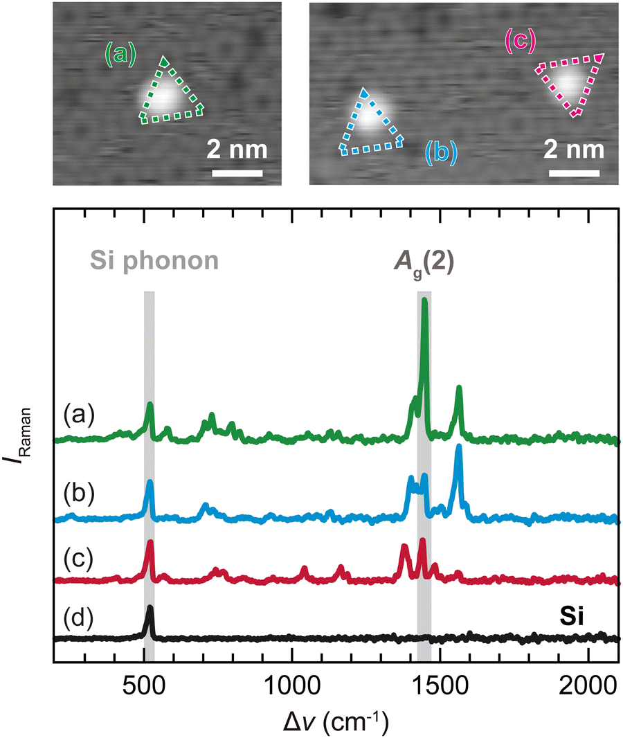 | ||
| Fig. 2 (a)–(c) TERS spectra (80 K, Vbias = 0.3 V, jSTM = 0.3 nA, λext = 532 nm, Pext = 5.5 mW, averaging time = 100 s) acquired over three C60 molecules with different adsorption sites. Insets: STM images (constant current mode, Vbias = 0.3 V, jSTM = 50 pA) of the molecules over which the spectra were recorded, with the same color-coding and labels (a)–(c) as those for the spectra. Triangles facing up (labelled as (a) and (b)) correspond to the unfaulted half unit cell, while the red triangle facing down (c) to the faulted one. (d) TERS spectrum over the bare Si(111)-(7 × 7) surface recorded with the identical acquisition conditions. See Fig. S2 (ESI†) for the spectra with the Si signal subtracted. | ||
The precise control of the tip–molecule distance in the STM junction enables us to examine the evolution of the TERS spectra as the tip approaches the molecule with picometer precision. Fig. 3 displays the evolution of the TERS spectra as the Ag tip sequentially approaches and retracts from a C60 molecule adsorbed on the same site as that in Fig. 2c. Fig. 3a shows the STM current jSTM as a function of the tip height Δz. The drastic change upon the MPC formation occurs simultaneously in jSTM and the Raman intensity, as highlighted in the waterfall plot of the approach–retract process (Fig. 3a–c). The spectral evolution is symmetric with respect to the turning point (Δz = −750 pm), indicating that the approach–retract process is reversible and the C60 remains intact. The TERS intensity exponentially increases as the tip approaches the molecule in the tunnelling regime. This increase is explained by the electromagnetic field enhancement in the STM junction as the tip–sample distance decreases.33 Once the MPC is formed, an abrupt increase of the TERS intensity and additional vibrational modes are observed, including the overtones and/or combination bands34 (see Fig. S4, ESI†). This phenomenon can also be observed on molecules on different adsorption sites, as shown in Fig. S5 (ESI†) for a C60 adsorbed on the unfaulted half unit cell. The change in the interaction between the carbon atoms in the deformed molecular cage and the underlying silicon atoms upon MPC formation likely results in an increased splitting of the molecular vibrations similar to that observed on Pt(111).25 We estimate the additional enhancement factor upon the MPC formation to be ∼30, based on the ratio of the TERS intensities of the Ag(2) peak measured 100 pm below and above the MPC, which is consistently observed for different adsorption sites. This enhancement factor is comparable to those observed in MPCs on noble metal surfaces.25 The strong enhancement occurs in both the Stokes and anti-Stokes branches (cf. Fig. 4). This observation suggests that the enhancement cannot be explained by a change of the plasmonic resonance in the STM junction, which may occur upon MPC formation, because the plasmonic resonance does not cover such a wide wavelength range. We ascribe it primarily to an additional chemical enhancement emerging from hybridization of the Si–C60 system with the metallic states in the tip, resulting in additional charge transfer and broadening of the molecular electronic states.25 The broadening and renormalization of molecular energy levels caused by hybridization impacts the static Raman polarizability, facilitates charge transfer within hybridized states, and affects the resonant Raman channels within the internal molecular levels.35,36 The relative intensity of certain TERS peaks varies between the tunnelling and MPC regimes, e.g. the ratio between Ag(2) and its adjacent peak at lower frequency in Fig. 3d, while it reverts back as the tip is retracted from the MPC. This reversibility rules out possible chemical transformations (e.g. decomposition) as the cause of the intensity change.19,37 Instead, this observation can be explained by subtle differences in the C60–Si covalent bonds after contact with the Ag tip. Minor changes in the adsorption geometry can lead to significant changes in the relative intensities of the TERS spectrum, as demonstrated in Fig. 2 and Fig. S3 (ESI†). Moreover, the sudden shift in the vibrational frequencies of the peaks, e.g. Ag(2) indicated by the dashed line in Fig. 3d, may be attributed to the additional charge transfer upon the MPC formation, with each mode being affected differently.38
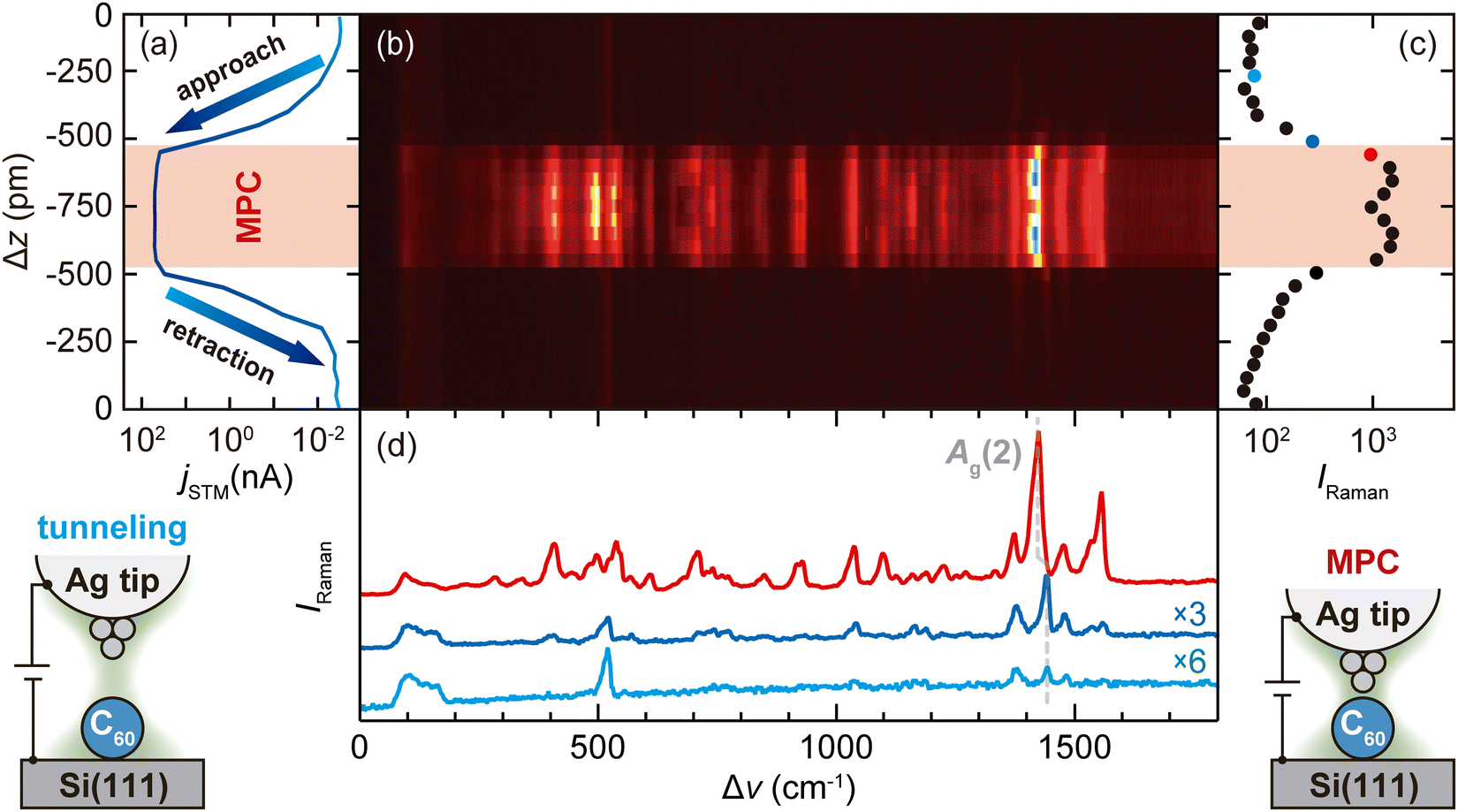 | ||
| Fig. 3 (a) jSTM–Δz curve showing the reversible transition from the tunnelling to the MPC regimes, where Δz = 0 corresponds to the set point corresponding to Vbias = 0.3 V and jSTM = 10 pA over the C60, with Vbias kept constant over the whole process. (b) Simultaneously recorded waterfall plot of TERS acquired during tip-approach and retraction over single C60 on faulted half unit cell of the Si(111)-(7 × 7) surface (80 K, setpoint: Vbias = 0.3 V and jSTM = 60 pA, λext = 532 nm, Pext = 5.5 mW, 5 s per spectrum, scale bar: arbitrary units). (c) Intensity of the Ag(2) mode in the different regimes highlighting the sudden increase upon MPC formation. (d) TERS spectra in the tunnelling and MPC regimes. The coloured points in (c) indicate where the spectrum in the same colour was recorded, and the grey dashed line highlights the shift of the Ag(2) mode upon MPC formation. | ||
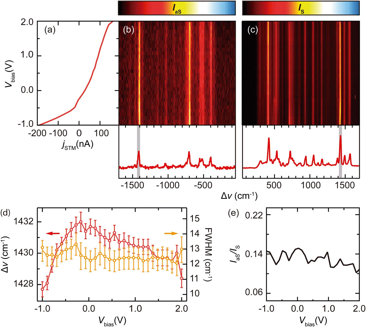 | ||
| Fig. 4 (a) jSTM–Vbias curve simultaneously acquired with the evolution of the TERS spectra in the MPC regime (80 K, setpoint: Vbias = 2.0 V and jSTM = 162.2 nA). (b) and (c) Waterfall plot of the Vbias-dependent TERS of a single C60 junction measured in the contact regime, simultaneously recording the anti-Stokes and Stokes branches (80 K, λext = 532 nm, Pext = 5.5 mW, 5 s per spectrum, scale bar for anti-Stokes IaS: arbitrary units, independent scale bar for Stokes IS: arbitrary units). The bottom panels correspond to selected Raman spectra in the anti-Stokes and Stokes branches from (b) and (c), respectively, at Vbias = −0.3 V and jSTM = 4.4 nA, with the Ag(2) mode highlighted in grey. (d) Peak position (red, left axis) and width (orange, right axis) of the Ag(2) mode as a function of Vbias, with the error bars extracted from the Gaussian fitting. (e) IaS/IS ratio of the Ag(2) mode as a function of Vbias. | ||
In the MPC regime, the anti-Stokes peaks of C60 are observed, allowing the investigation of vibrational heating in single-molecule junctions17 (Fig. 4). In the case of C60 both in the tunnelling and MPCs regimes on metal surfaces, it has been shown that strong vibrational heating occurs via inelastic electron–vibration scattering.17,18 Fig. 4a displays the jSTM–Vbias characteristic of a single C60 junction on the Si(111)-(7 × 7) surface with simultaneously tracking the anti-Stokes and Stokes branches (Fig. 4b and c, respectively), with single spectra of both branches depicted in Fig. 4d and e. Since thermal excitation of the C60 vibrations is negligible at 80 K (∼7 meV), an external energy input must be present. The appearance of the anti-Stokes peaks even at zero current indicates that the vibrationally excited states are significantly populated through optical excitation of the MPC junction, further enhanced by the plasmonic response.39,40 However, unlike the case for metal surfaces, there is no obvious indication of vibrational heating through inelastic electron–vibration scattering in the Ag tip–C60–Si junction, which should be manifested as a simultaneous redshift and broadening of vibrational peaks as well as an increase in the anti-Stokes to the Stokes ratio.18 The redshift and broadening are caused by an increase in the anharmonicity of the vibrational modes due to considerable heating of the molecule,41 while the increase of the IaS/IS ratio results from a higher population of excited states. In the present case, we observe a minor peak shift of few cm−1 in the peak position of the high-frequency vibrational mode such as Ag(2) (Fig. 4f, red), which is an order of magnitude smaller than what is observed for metal–C60–metal junctions. Consequently, no peak broadening is expected, suggesting that vibrational heating through inelastic electron–vibration scattering is not significant in metal–C60–Si junctions18 (Fig. 4f, orange). Therefore, the quasi-symmetric behaviour of the peak position cannot be rationalized by vibrational heating within C60. In current-carrying C60 junctions, bias-voltage-driven charging effects typically result in a quadratic behaviour,42,43 while the vibrational Stark effect exhibits a linear dependence on the applied electric field. Small variations of the peak position can also be attributed to mechanical deformation accompanied with the MPC.25 Thus, we tentatively attribute the peak shift in Fig. 4f (ca. 4 cm−1) to the consequence of the interplay between these three factors. The minimal variation in the anti-Stokes to Stokes ratio (IaS/IS) as a function of Vbias in Fig. 4g further indicates the inefficiency of vibrational heating. The absence of significant vibrational heating is primarily due to a much smaller current density in the MPC on the Si(111)-(7 × 7) surface compared to that in the MPCs on metal surfaces (about one order of magnitude). We would like to note that the vibrational decay mechanisms could also differ from those on metal surfaces. In a metal–C60–metal junction the creation of electron–hole pairs (EHP) dominates the cooling mechanism, as the phonon-mediated mechanism is much slower due to the large energy mismatch between the molecular vibrations (33 to 200 meV) and the phonon bandwidths of the substrates (Ag, 22 meV; Au, 16 meV; Cu, 30 meV; Pt, 24 meV).44,45 Alternatively, in the case of the Si(111)-(7 × 7), the intense optical phonon mode of the bulk lies at 65 meV and the Debye cutoff appears up to 68 meV,46 facilitating the decay of molecular vibrations to the lattice oscillations.
Conclusions
We conducted TERS measurements for single C60 molecules adsorbed on the Si(111)-(7 × 7) reconstructed surface. The molecules adsorb onto several different sites and orientations, each exhibiting different spectral features. The spatial distribution of the TERS intensity within a single C60 shows a distribution that could be attributed to sub-molecular feature. In addition, a large enhancement of Raman scattering, reaching ∼1012, is quantified in the tunnelling regime by comparing it to the Raman intensity of the optical phonon mode of the bulk Si. This enhancement involves contributions from both electromagnetic and chemical mechanisms. Furthermore, we showed that Raman scattering can be further enhanced by a factor of ∼30 when a MPC is formed between the tip and a single C60, comparable to those observed on metal substrates. In the MPC regime, additional Raman peaks emerge, including overtone and combination bands. Additionally, the anti-Stokes peaks are also observed in the MPC junction at 80 K, indicating that the vibrationally excited states are populated by an external energy input. The optically induced vibrational excitation is evidenced by the appearance of the anti-Stokes peaks at zero current, whereas vibrational excitation by current flow is negligible. Our findings demonstrate the applicability of TERS to the characterization of organic molecules on semiconductor surfaces and potentially to single-molecule Raman thermometry studying vibrational heating and dissipation in current-carrying metal–molecule–semiconductor nanojunctions.Data availability
Data for this article are available at Zenodo at https://doi.org/10.5281/zenodo.12517248.Conflicts of interest
There are no conflicts to declare.Acknowledgements
The authors acknowledge Adnan Hammud for providing the Ag tips prepared with focused ion beam. B. C. acknowledges support from Spanish CM “Talento Program César Nombela” (project No. 2023-T1/TEC-28968), PID2021-125309OA-100 and CSIC-20226AT011. I. H. acknowledges the support of JSPS KAKENHI Grant No. JP20H05660. T. K. acknowledges the support of JST FOREST Grant No. JPMJFR201J and JSPS KAKENHI Grant No. JP19K24684.References
- A. Vilan and D. Cahen, Chem. Rev., 2017, 117, 4624–4666 CrossRef CAS PubMed.
- A. Sweetman, S. P. Jarvis, P. Rahe, N. R. Champness, L. Kantorovich and P. Moriarty, Phys. Rev. B: Condens. Matter Mater. Phys., 2014, 90, 165425 CrossRef.
- J. Repp, G. Meyer, S. M. Stojković, A. Gourdon and C. Joachim, Phys. Rev. Lett., 2005, 94, 026803 CrossRef PubMed.
- L. Liu, S. Liu, X. Chen, C. Li, J. Ling, X. Liu, Y. Cai and L. Wang, Sci. Rep., 2013, 3, 3062 CrossRef PubMed.
- R. Gutzler, M. Garg, C. R. Ast, K. Kuhnke and K. Kern, Nat. Rev. Phys., 2021, 3, 441–453 CrossRef.
- T. Itoh, M. Procházka, Z.-C. Dong, W. Ji, Y. S. Yamamoto, Y. Zhang and Y. Ozaki, Chem. Rev., 2023, 123, 1552–1634 CrossRef CAS PubMed.
- B. Yang, G. Chen, A. Ghafoor, Y. Zhang, Y. Zhang, Y. Zhang, Y. Luo, J. Yang, V. Sandoghdar, J. Aizpurua, Z. Dong and J. G. Hou, Nat. Photonics, 2020, 14, 693–699 CrossRef CAS.
- J. Lee, K. T. Crampton, N. Tallarida and V. A. Apkarian, Nature, 2019, 568, 78–82 CrossRef CAS PubMed.
- J. Xu, X. Zhu, S. Tan, Y. Zhang, B. Li, Y. Tian, H. Shan, X. Cui, A. Zhao, Z. Dong, J. Yang, Y. Luo, B. Wang and J. G. Hou, Science, 2021, 371, 818–822 CrossRef CAS PubMed.
- H. Imada, M. Imai-Imada, K. Miwa, H. Yamane, T. Iwasa, Y. Tanaka, N. Toriumi, K. Kimura, N. Yokoshi, A. Muranaka, M. Uchiyama, T. Taketsugu, Y. K. Kato, H. Ishihara and Y. Kim, Science, 2021, 373, 95–98 CrossRef CAS PubMed.
- M. Imai-Imada, H. Imada, K. Miwa, Y. Tanaka, K. Kimura, I. Zoh, R. B. Jaculbia, H. Yoshino, A. Muranaka, M. Uchiyama and Y. Kim, Nature, 2022, 603, 829 CrossRef CAS PubMed.
- A. Rosławska, K. Kaiser, M. Romeo, E. Devaux, F. Scheurer, S. Berciaud, T. Neuman and G. Schull, Nat. Nanotechnol., 2024, 19, 738–743 CrossRef PubMed.
- M. Garg, A. Martín-Jiménez, M. Pisarra, Y. Luo, F. Martín and K. Kern, Nat. Photonics, 2022, 16, 196–202 CrossRef CAS.
- M. K. Schmidt, R. Esteban, A. González-Tudela, G. Giedke and J. Aizpurua, ACS Nano, 2016, 10, 6291–6298 CrossRef CAS PubMed.
- S. Liu, A. Hammud, M. Wolf and T. Kumagai, Nano Lett., 2021, 21, 4061 Search PubMed.
- R.-P. Wang, C.-R. Hu, Y. Han, B. Yang, G. Chen, Y. Zhang, Y. Zhang and Z.-C. Dong, J. Phys. Chem. C, 2022, 126, 12121–12128 CrossRef CAS.
- D. R. Ward, D. A. Corley, J. M. Tour and D. Natelson, Nat. Nanotechnol., 2011, 6, 33–38 CrossRef CAS PubMed.
- B. Cirera, M. Wolf and T. Kumagai, ACS Nano, 2022, 16, 16443–16451 CrossRef CAS PubMed.
- Q. Meng, J. Zhang, Y. Zhang, W. Chu, W. Mao, Y. Zhang, J. Yang, Y. Luo, Z. Dong and J. G. Hou, Sci. Adv., 2024, 10, eadl1015 CrossRef CAS PubMed.
- J. I. Pascual, J. Gómez-Herrero, C. Rogero, A. M. Baró, D. Sánchez-Portal, E. Artacho, P. Ordejón and J. M. Soler, Chem. Phys. Lett., 2000, 321, 78–82 CrossRef CAS.
- R. Rurali, R. Cuadrado and J. I. Cerdá, Phys. Rev. B: Condens. Matter Mater. Phys., 2010, 81, 075419 CrossRef.
- S. Gangopadhyay, R. A. J. Woolley, R. Danza, M. A. Phillips, K. Schulte, L. Wang, V. R. Dhanak and P. J. Moriarty, Surf. Sci., 2009, 603, 2896–2901 CrossRef CAS.
- P. Avouris and R. Wolkow, Phys. Rev. B: Condens. Matter Mater. Phys., 1989, 39, 5091–5100 CrossRef CAS PubMed.
- J. H. Parker, D. W. Feldman and M. Ashkin, Phys. Rev., 1967, 155, 712–714 CrossRef CAS.
- B. Cirera, Y. Litman, C. Lin, A. Akkoush, A. Hammud, M. Wolf, M. Rossi and T. Kumagai, Nano Lett., 2022, 22, 2170–2176 CrossRef CAS PubMed.
- S. Liu, B. Cirera, Y. Sun, I. Hamada, M. Müller, A. Hammud, M. Wolf and T. Kumagai, Nano Lett., 2020, 20, 5879–5884 CrossRef CAS PubMed.
- S. Liu, M. Müller, Y. Sun, I. Hamada, A. Hammud, M. Wolf and T. Kumagai, Nano Lett., 2019, 19, 5725–7731 CrossRef CAS PubMed.
- C. Muehlethaler, C. R. Considine, V. Menon, W.-C. Lin, Y.-H. Lee and J. R. Lombardi, ACS Photonics, 2016, 3, 1164–1169 CrossRef CAS.
- X. Du, F. Chen, X. Chen, X. Wu, Y. Cai, X. Liu and L. Wang, Appl. Phys. Lett., 2010, 97, 253106 CrossRef.
- J. Y. Lee and M. H. Kang, Surf. Sci., 2008, 602, 1408–1412 CrossRef CAS.
- J. G. Hou, J. Yang, H. Wang, Q. Li, C. Zeng, H. Lin, W. Bing, D. M. Chen and Q. Zhu, Phys. Rev. Lett., 1999, 83, 3001–3004 CrossRef CAS.
- K. Sakamoto, M. Harada, D. Kondo, A. Kimura, A. Kakizaki and S. Suto, Phys. Rev. B: Condens. Matter Mater. Phys., 1998, 58, 13951–13956 CrossRef CAS.
- S. Liu, F. P. Bonafé, H. Appel, A. Rubio, M. Wolf and T. Kumagai, ACS Nano, 2023, 17, 10172–10180 CrossRef CAS PubMed.
- J. Menéndez and J. B. Page, in Light Scattering in Solids VIII: Fullerenes, Semiconductor Surfaces, Coherent Phonons, eds. M. Cardona and G. Güntherodt, Springer Berlin Heidelberg, 2000, pp. 27–95 Search PubMed.
- L. Jensen, C. M. Aikens and G. C. Schatz, Chem. Soc. Rev., 2008, 37, 1061–1073 RSC.
- J. Langer, D. Jimenez de Aberasturi, J. Aizpurua, R. A. Alvarez-Puebla, B. Auguié, J. J. Baumberg, G. C. Bazan, S. E. J. Bell, A. Boisen, A. G. Brolo, J. Choo, D. Cialla-May, V. Deckert, L. Fabris, K. Faulds, F. J. García de Abajo, R. Goodacre, D. Graham, A. J. Haes, C. L. Haynes, C. Huck, T. Itoh, M. Käll, J. Kneipp, N. A. Kotov, H. Kuang, E. C. Le Ru, H. K. Lee, J.-F. Li, X. Y. Ling, S. A. Maier, T. Mayerhöfer, M. Moskovits, K. Murakoshi, J.-M. Nam, S. Nie, Y. Ozaki, I. Pastoriza-Santos, J. Pérez-Juste, J. Popp, A. Pucci, S. Reich, B. Ren, G. C. Schatz, T. Shegai, S. Schlücker, L.-L. Tay, K. G. Thomas, Z.-Q. Tian, R. P. Van Duyne, T. Vo-Dinh, Y. Wang, K. A. Willets, C. Xu, H. Xu, Y. Xu, Y. S. Yamamoto, B. Zhao and L. M. Liz-Marzán, ACS Nano, 2020, 14, 28–117 CrossRef CAS PubMed.
- G. Schulze, K. J. Franke, A. Gagliardi, G. Romano, C. S. Lin, A. L. Rosa, T. A. Niehaus, Th Frauenheim, A. Di Carlo, A. Pecchia and J. I. Pascual, Phys. Rev. Lett., 2008, 100, 136801 CrossRef CAS PubMed.
- P. Zhou, K.-A. Wang, Y. Wang, P. C. Eklund, M. S. Dresselhaus, G. Dresselhaus and R. A. Jishi, Phys. Rev. B: Condens. Matter Mater. Phys., 1992, 46, 2595–2605 CrossRef CAS PubMed.
- R. C. Maher, C. M. Galloway, E. C. Le Ru, L. F. Cohen and P. G. Etchegoin, Chem. Soc. Rev., 2008, 37, 965–979 RSC.
- C. Zhan, J. Yi, S. Hu, X.-G. Zhang, D.-Y. Wu and Z.-Q. Tian, Nat. Rev. Methods Primers, 2023, 3, 12 CrossRef CAS.
- A. V. Talyzin, A. Dzwilewski and T. Wågberg, Solid State Commun., 2006, 140, 178–181 CrossRef CAS.
- Y. Li, P. Zolotavin, P. Doak, L. Kronik, J. B. Neaton and D. Natelson, Nano Lett., 2016, 16, 1104–1109 CrossRef CAS PubMed.
- Y. Li, P. Doak, L. Kronik, J. B. Neaton and D. Natelson, Proc. Natl. Acad. Sci., 2014, 111, 1282–1287 CrossRef CAS PubMed.
- M. Persson and B. Hellsing, Phys. Rev. Lett., 1982, 49, 662–665 CrossRef CAS.
- S. Kumar, H. Jiang, M. Schwarzer, A. Kandratsenka, D. Schwarzer and A. M. Wodtke, Phys. Rev. Lett., 2019, 123, 156101 CrossRef CAS PubMed.
- J. Kim, M.-L. Yeh, F. S. Khan and J. W. Wilkins, Phys. Rev. B: Condens. Matter Mater. Phys., 1995, 52, 14709–14718 CrossRef CAS PubMed.
Footnotes |
| † Electronic supplementary information (ESI) available. See DOI: https://doi.org/10.1039/d4cp01803f |
| ‡ Equally contributing. |
| This journal is © the Owner Societies 2024 |