
Ionic liquid enables high-performance, self-powered CsPbBr3 perovskite nanonet photodetector†
Hai
Zhou
 *abc,
Rui
Wang
ac,
Xuhui
Zhang
ac,
Bo’ao
Xiao
ac,
Zihao
Shuang
a,
Dingjun
Wu
a and
Pingli
Qin
*b
*abc,
Rui
Wang
ac,
Xuhui
Zhang
ac,
Bo’ao
Xiao
ac,
Zihao
Shuang
a,
Dingjun
Wu
a and
Pingli
Qin
*b
aInternational School of Microelectronics, Dongguan University of Technology, Dongguan, Guangdong 523808, China. E-mail: hizhou@dgut.edu.cn
bHubei Key Laboratory of Optical Information and Pattern Recognition, Wuhan Institute of Technology, Wuhan, 430205, China. E-mail: qpl2015@wit.edu.cn
cFaculty of Physics & Electronic Science, Hubei University, Wuhan, 430062, China
First published on 6th June 2023
Abstract
We fabricated high-quality CsPbBr3 perovskite nanonet films with the assistance of polystyrene spheres, and constructed self-powered photodetectors (PDs) with an ITO/SnO2/CsPbBr3/carbon structure. By passivating the nanonet with different concentrations of 1-butyl-3-methylimidazolium bromide (BMIMBr) ionic liquid, we found that as the concentration of BMIMBr increases, the dark current of the device first decreases and then gradually increases, while the photocurrent remains essentially unchanged. Finally, the PD with 1 mg mL−1 BMIMBr ionic liquid exhibited the best performance with a switch ratio of about 1.35 × 10⁶, a linear dynamic range extending to 140 dB, and responsivity and detectivity values of 0.19 A W−1 and 4.31 × 10¹² Jones, respectively. These results provide an important reference for fabricating perovskite PDs.
CsPbBr3 perovskite not only has the unique advantages of the perovskite family, such as simple preparation process and high charge carrier mobility, its all-inorganic structure is more stable than those of organic–inorganic and two-dimensional perovskites, showing great potential in fields such as solar cells, PDs, and light-emitting diodes.1–5 However, the rapid solvent evaporation and crystallization during the preparation of perovskite films usually result in poor crystallinity, high defect density, pinholes, and small grain size, which decrease the performance and stability of perovskite PDs.6,7 Therefore, controlling the crystallization rate of CsPbBr3 perovskite has become an effective means of improving the quality of its films.7–9 In addition, severe charge recombination processes take place at the interface of the device and the grain boundaries of perovskite crystals, which result in the degradation of device performance. Therefore, passivating the defects of the perovskite absorber layer is also a key factor in improving the performance of perovskite optoelectronic devices.10–17
Ionic liquids, as an excellent type of material, have been reported to efficiently passivate the defects of perovskites18–22 due to the existence of BMIMBr, which can passivate the related deep traps induced by the halide in CsPbBr3 because the positive electron density of the organic cation [BMIM]+ can acquire electrons from the under-coordinated Br− and the Pb–Br antisite defects (PbBr3−). Besides, the high negative electron density of the inorganic anion [BBr4]− enables its incorporation into the lattice structure of CsPbBr3 to compensate Br vacancies and passivate unsaturated-Pb-related defects in CsPbBr3. More importantly, ionic liquids show many advantages: (1) they contain a large number of asymmetric organic cations, such as imidazole, phosphorus, and pyridine, which combine with organic or inorganic anions of opposite polarity, such as COOH−, CF3COO−, BF4−, Cl−, and I−; (2) ionic liquids are composed entirely of ions, so they have good conductivity and thermal stability, as well as good solubility, low toxicity, and low flammability, making them an ideal material for optoelectronic passivation; (3) ionic liquids are hydrophobic, so using them as additives is an effective way of adjusting the hydrophobicity of precursor solutions and prevent water penetration.
Owing to the advantages of high-quality film formation based on crystal growth rate control and efficient passivation of defects by ionic liquids, we have employed polystyrene (PS) spheres as a template to control the crystallization rate of the perovskite for fabricating high-quality CsPbBr3 perovskite nanonet films, and then 1-butyl-3-methylimidazolium bromide (BMIMBr ionic liquid) is chosen for passivating the CsPbBr3 perovskite nanonet with different concentrations due to its great improvement to our device performance and stability in our previous work20,21, and finally a self-powered PD with an ITO/SnO2/CsPbBr3/carbon structure is constructed. By analyzing the photo/dark current of the PDs passivated with different concentrations of BMIMBr ionic liquid, it was found that as the concentration of BMIMBr ionic liquid increased, the dark current of the device first decreased and then gradually increased, while the photocurrent remained essentially unchanged. Finally, the device containing 1 mg mL−1 BMIMBr ionic liquid displayed the best performance, achieving a switch ratio of approximately 1.35 × 10⁶, an impressive linear dynamic range (LDR) of 140 dB, a responsivity (R) of 0.19 A W−1, and detectivity (D*) of 4.31 × 10¹² Jones. These results provide a reference value for fabricating perovskite PDs.
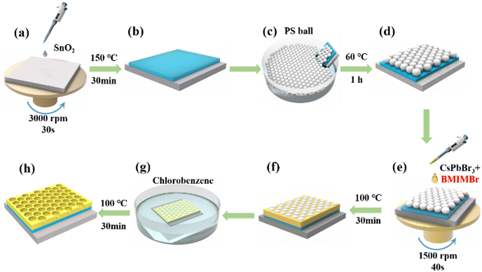
A schematic diagram of the fabrication process for the CsPbBr3 perovskite nanonet is presented in Fig. 1, with a more detailed description available in our previous work23 and the experimental section. To begin with, SnO2 solution was dispensed onto the ITO substrate that had been treated, and then spin-coated at 3000 rpm for 30 seconds. Then, single-layered PS microspheres were coated on the SnO2/ITO substrate for the subsequent preparation of the perovskite. To investigate the effect of BMIMBr ionic liquid on the CsPbBr3 perovskite nanonet PD, different concentrations of BMIMBr ionic liquid were added to the CsPbBr3 precursor solution to obtain the optimal concentration. Then, the precursor solution was dropped onto a SnO2/ITO substrate with PS spheres. The substrate was then spin-coated and annealed on a heating stage for 30 min. After that, the CsPbBr3 film was submersed in a glass bottle containing chlorobenzene to eliminate the PS spheres. Finally, the carbon electrodes were fabricated on the sample surface using screen printing technology, and the CsPbBr3 nanonet PDs were fabricated with an ITO/SnO2/CsPbBr3/carbon structure, and the active area of the device is 0.2 × 0.2 cm2.
 | ||
| Fig. 1 Schematic diagram of the fabrication process for the CsPbBr3 perovskite nanonet. | ||
The SEM images in Fig. 2a depict cross-sectional and top views of single-layer PS spheres on our substrates, confirming their uniformity, and clearly showing that the PS spheres on our substrates are in a single layer. With the assistance of these single-layer PS spheres, we obtained the perovskite nanonet film, whose surface morphology is as shown in Fig. 2b while Fig. 2c shows the corresponding cross-sectional SEM image. During the experiment, it was observed that a nanonet hollow structure could be created in all CsPbBr3 films, regardless of the presence or absence of the ionic liquid (as indicated in Fig. S1, ESI†), after removing the PS microspheres. Additionally, the resulting nanonet film had a thickness of approximately 1 μm. The uniformly dense nanonet can effectively reduce light reflection and improve light utilization efficiency, and provides better photoelectric detection performance.6
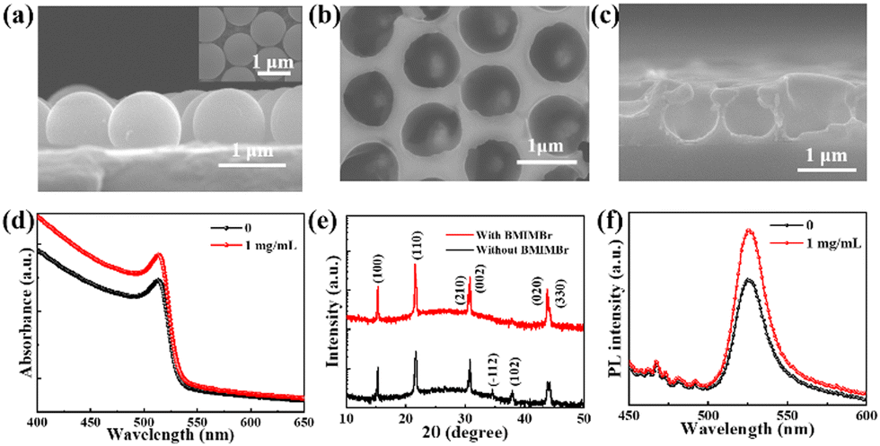 | ||
| Fig. 2 (a) Cross-sectional SEM image of single-layer PS spheres; the inset shows the top view SEM image of single-layer PS spheres. Top (b) and cross-sectional (c) SEM image of the CsPbBr3 perovskite nanonet film with BMIMBr ionic liquid. (d) Absorption spectra of the CsPbBr3 perovskite nanonet films. (e) XRD patterns of the CsPbBr3 perovskite nanonet films. (f) Steady-state PL spectra of the CsPbBr3 perovskite nanonet films. | ||
The light absorption curves of the CsPbBr3 films with and without the inclusion of BMIMBr ionic liquid are presented in Fig. 2d. From the figure, the CsPbBr3 film with BMIMBr ionic liquid shows a higher absorption peak, which can be attributed to the improved crystalline quality of the CsPbBr3 film with the addition of BMIMBr ionic liquid. Fig. 2e shows the X-ray diffraction (XRD) patterns of CsPbBr3 films with and without the addition of BMIMBr ionic liquid. From the XRD patterns, the characteristic peaks of the CsPbBr3 films have higher intensity after the addition of BMIMBr, particularly the (110) peak, indicating that the fabricated CsPbBr3 nanonet film after the addition of BMIMBr has higher crystal quality, which is conducive to achieving excellent device performance. The steady-state photoluminescence (PL) spectra of the CsPbBr3 films are shown in Fig. 2f. Under excitation by a 320 nm laser, the CsPbBr3 film incorporating BMIMBr exhibits a significantly greater PL intensity compared to that without BMIMBr, suggesting that the CsPbBr3 film based on BMIMBr has reduced defect density and superior crystalline quality.21,24
Fig. 3a shows the schematic structure of the nanonet-structured CsPbBr3 PD, which consists of ITO/SnO2/nanonet-structured CsPbBr3/carbon layers. The presence of the nanonet-structured hollow CsPbBr3 film effectively increases the surface area of the film and reduces light reflection, leading to better utilization of light.16 To investigate the optimal concentration of BMIMBr ionic liquid to improve the performance of the nanonet-structured CsPbBr3 PDs, 0/0.5/1/2/5 mg mL−1 BMIMBr ionic liquid was added to the precursor solution. Good photoelectric performance was exhibited by all devices, as depicted in Fig. 3b. With the increase of the BMIMBr ionic liquid concentration, the dark current density of the devices decreased first and then gradually increased, while the photocurrent density remained almost unchanged. For the changes to the dark current density, we think the reduced dark current density is attributed to the reduction of the Br vacancies by adding BMIMBr. However, with further increasing the concentration of BMIMBr, more BMIMBr leads to more Br ions, which increases the conductivity of the device and finally increases the dark current density of the device. Compared with the devices using other concentrations of ionic liquids, the device using 1 mg mL−1 BMIMBr ionic liquid has the lowest dark current density, maximum photocurrent density, and more concentrated statistical data distribution with higher repeatability. Therefore, 1 mg mL−1 was chosen as the optimal concentration of BMIMBr ionic liquid.
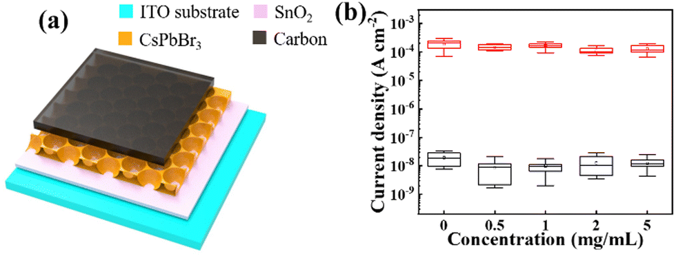 | ||
| Fig. 3 (a) Schematic structure of the CsPbBr3 nanonet PD. (b) Light and dark current statistics of the CsPbBr3 nanonet PDs with various concentrations of BMIMBr ionic liquid. | ||
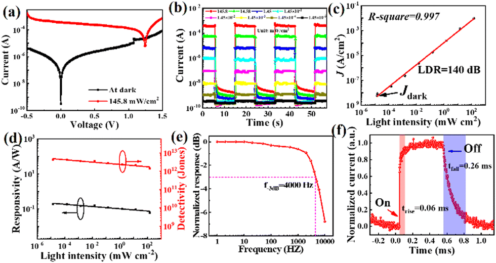
The characteristic current–voltage (I–V) curves of the CsPbBr3 nanonet PDs with the optimal BMIMBr ionic liquid (1 mg mL−1) are shown in Fig. 4a. From the curves, the device exhibits good rectifying characteristics and has good self-powered ability, with an open-circuit voltage of 1.24 V under 145 mW cm−2 illumination. The current–time (I–t) curves of the CsPbBr3 nanonet PDs with the optimal BMIMBr ionic liquid under different light intensities at 0 V are shown in Fig. 4b. As the light power increases from 1.45 × 10⁻⁵ to 145.8 mW cm−2, the photocurrent also gradually increases, showing a positive correlation. At the same time, the dark current of the device is extremely low, at about 2.51 × 10⁻¹⁰ A, while the photocurrent at the maximum light power reaches 3.4 × 10⁻⁴ A, and the on–off ratio of the device can be calculated to be about 1.35 × 10⁶. Besides, there is a certain fluctuation in the dark current, we think the main reason is attributed to the existence of the defect in the perovskite. When the device is illuminated by light, a large number of photo-generated carriers will be generated, and some of them may be trapped by these defects and remain. After the light is removed, these remaining photo-generated carriers will be slowly released and cause the increase of the dark current. When stronger light is applied, more photo-generated carriers are generated and more are left, resulting in the dark current fluctuating under different light intensities.
 | ||
| Fig. 4 The performance of the CsPbBr3 nanonet PD with the optimal BMIMBr ionic liquid concentration (1 mg mL−1): (a) I–V curves; (b) I–t curves at different light intensities; (c) LDR; (d) R and D*; (e) f−3dB bandwidth; (f) response speed. | ||
The correlation between the light intensity and photocurrent density is illustrated in Fig. 4c. By using the formula 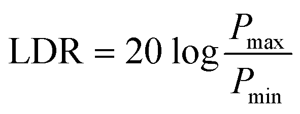 , where Pmax (Pmin) is the incident light intensity above (below) which the photocurrent begins to deviate from linearity, the LDR of the device can be calculated with a value of up to 140 dB. In addition, by linearly fitting the data, the R-square of the device is 0.997, which is very close to 1, indicating good linearity in the measurement range. Based on the formulas
 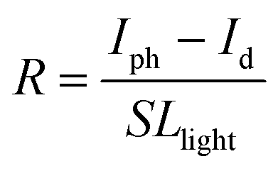 and
and 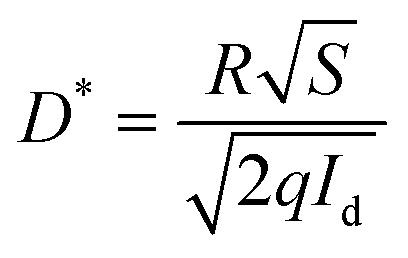 , the R and D* curves are plotted in Fig. 4d, indicating a decrease in the R and D* values with increasing light intensity. Under irradiation of 1.45 × 10⁻⁵ mW cm−2, the maximum R and D* of the device are 0.19 A W−1 and 4.31 × 10¹² Jones (1 Jones = 1 cm Hz1/2 W−1), respectively. These values are comparable to those of the most advanced perovskite PDs (the detailed comparison is shown in Table S1, ESI†),25–27 showing that the nanonet-structured CsPbBr3 PD with the optimal BMIMBr ionic liquid concentration exhibits excellent photodetection ability.
To measure the frequency response of the device, an optical chopper was used to change the frequency of the incident light (1 Hz–10 kHz), and the resulting f−3dB curve is depicted in Fig. 4e. As the frequency increases, the waveform gradually changes from a square wave to a triangular wave, and the f−3dB of the device is about 4 kHz. In addition, it can be seen from the fast response I–t curve (Fig. 4f) that the rise and fall times (τrise and τfall) of the optimal BMIMBr ionic liquid concentration CsPbBr3 nanonet PD are 0.06 ms and 0.26 ms, respectively, indicating a fast response speed.
In conclusion, we introduced PS spheres to assist in the preparation of high-quality CsPbBr3 perovskite nanonet films, and explored the effect of different concentrations of BMIMBr ionic liquid on the performance of the nanonet-structured CsPbBr3 PD. The results showed that the device with the optimal concentration of BMIMBr ionic liquid had better crystallization and optimal photoelectric performance, with a switch ratio of about 1.35 × 10⁶ and an LDR of 140 dB. The device reached maximum R and D* values of 0.19 A W−1 and 4.31 × 10¹² Jones, respectively, when irradiated at 1.45 × 10⁻⁵ mW cm−2. These results provide a reference for fabricating perovskite PDs.
This work was supported by the National Natural Science Foundation of China (No. 51972101), the Research Platforms and Projects of Guangdong Universities in 2022 (No. 2022ZDZX1028), and Hubei Key Laboratory of Optical Information and Pattern Recognition, Wuhan Institute of Technology (No. 202206).
Conflicts of interest
The authors declare that they have no conflict of interest.Notes and references
- C. Xie, C. K. Liu, H. L. Loi and F. Yan, Adv. Funct. Mater., 2020, 30(20), 1903907 CrossRef CAS.
- C. Xie, P. You, Z. Liu, L. Li and F. Yan, Light Sci. Appl., 2017, 6(8), e17023–e17023 CrossRef.
- H. Zhou, Z. Song, C. R. Grice, C. Chen, J. Zhang, Y. Zhu, R. Liu, H. Wang and Y. Yan, Nano Energy, 2018, 53, 880–886 CrossRef CAS.
- X. Pan, J. Zhang, H. Zhou, R. Liu, D. Wu, R. Wang, L. Shen, L. Tao, J. Zhang and H. Wang, Nano-Micro Lett., 2021, 13, 1–12 CrossRef CAS.
- G. Li, Y. Wang, L. Huang and W. Sun, ACS Appl. Electron. Mater., 2022, 4(4), 1485–1505 CrossRef CAS.
- R. Liu, H. Zhou, Z. Song, X. Yang, D. Wu, Z. Song, H. Wang and Y. Yan, Nanoscale, 2019, 11(19), 9302–9309 RSC.
- J. Zeng, X. Li, Y. Wu, D. Yang, Z. Sun, Z. Song, H. Wang and H. Zeng, Adv. Funct. Mater., 2018, 28(43), 1804394 CrossRef.
- X. Zeng, W. Li, C. Yan, J. Cao, X. Fu and W. Yang, J. Mater. Chem. C, 2021, 9(44), 15967–15976 RSC.
- Y. Ren, Y. Hao, N. Zhang, Z. Arain, M. Mateen, Y. Sun, P. Shi, M. Cai and S. Dai, Chem. Eng. J., 2020, 392, 123805 CrossRef CAS.
- W. Zhao, P. Guo, J. Su, Z. Fang, N. Jia, C. Liu, L. Ye, Q. Ye, J. Chang and H. Wang, Adv. Funct. Mater., 2022, 32(24), 2200534 CrossRef CAS.
- J. Xu, J. Cui, S. Yang, Y. Han, X. Guo, Y. Che, D. Xu, C. Duan, W. Zhao, K. Guo and W. Ma, Nano-Micro Lett., 2022, 14(1), 7 CrossRef CAS PubMed.
- W. Dong, W. Qiao, S. Xiong, J. Yang, X. Wang, L. Ding, Y. Yao and Q. Bao, Nano-Micro Lett., 2022, 14(1), 108 CrossRef CAS.
- R. Lin, J. Xu, M. Wei, Y. Wang, Z. Qin, Z. Liu, J. Wu, K. Xiao, B. Chen, S. M. Park and G. Chen, Nature, 2022, 603(7899), 73–78 CrossRef CAS PubMed.
- J. Wang, L. Liu, S. Chen, L. Qi, M. Zhao, C. Zhao, J. Tang, X. Cai, F. Lu and T. Jiu, Small, 2022, 18(3), 2104100 CrossRef CAS PubMed.
- Y. He, M. Petryk, Z. Liu, D. G. Chica, I. Hadar, C. Leak and M. G. Kanatzidis, Nat. Photonics, 2021, 15(1), 36–42 CrossRef CAS.
- L. Zhao, Y. Zhou, Z. Shi, Z. Ni, M. Wang, Y. Liu and J. Huang, Nat. Photonics, 2023, 17(4), 315–323 CrossRef CAS.
- Y. Zhou, C. Fei, M. A. Uddin, L. Zhao, Z. Ni and J. Huang, Nature, 2023, 1–7 Search PubMed.
- F. Wang, C. Y. Ge, D. Duan, H. Lin, L. Li, P. Naumov and H. Hu, Small Structures, 2022, 3(8), 2200048 CrossRef CAS.
- H. Peng, D. Li, Z. Li, Z. Xing, X. Hu, T. Hu and Y. Chen, Nano-Micro Lett., 2023, 15(1), 91 CrossRef CAS PubMed.
- Z. Gao, H. Zhou, K. Dong, C. Wang, J. Wei, Z. Li, J. Li, Y. Liu, J. Zhao and G. Fang, Nano-Micro Lett., 2022, 14(1), 215 CrossRef CAS.
- D. Wu, Y. Xu, H. Zhou, X. Feng, J. Zhang, X. Pan, Z. Gao, R. Wang, G. Ma, L. Tao, H. Wang, J. Duan, H. Wan, J. Zhang, L. Shen, H. Wang and T. Zhai, InfoMat, 2022, 4(9), e12320 CrossRef CAS.
- L. Gu, C. Ran, L. Chao, Y. Bao, W. Hui, Y. Wang, Y. Chen, X. Gao and L. Song, ACS Appl. Mater. Interfaces, 2022, 14(20), 22870–22878 CrossRef CAS PubMed.
- R. Wang, H. Zhou, B. Wu, D. Wu, L. Tao, H. Wang, X. Peng, J. Zhang and H. Wang, J. Phys. Chem. Lett., 2021, 12(31), 7519–7525 CrossRef CAS PubMed.
- M. Du, X. Zhu, L. Wang, H. Wang, J. Feng, X. Jiang, Y. Cao, Y. Sun, L. Duan, Y. Jiao, K. Wang, X. Ren, Z. Yan, S. Pang and S. Liu, Adv. Mater., 2020, 32(47), 2004979 CrossRef CAS.
- Z. Shuang, H. Zhou, D. Wu, X. Zhang, B. Xiao, G. Ma, J. Zhang and H. Wang, Chem. Eng. J., 2022, 433, 134544 CrossRef CAS.
- J. Yan, Y. Li, F. Gao, W. Gong, Y. Tian and L. Li, J. Mater. Chem. C, 2022, 10(23), 8922–8930 RSC.
- W. Kim, J. Park, Y. Aggarwal, S. Sharma, E. H. Choi and B. Park, Nanomaterials, 2023, 13(3), 619 CrossRef CAS.
Footnote |
| † Electronic supplementary information (ESI) available. See DOI: https://doi.org/10.1039/d3cc02094k |
| This journal is © The Royal Society of Chemistry 2023 |