
 Open Access Article
 This Open Access Article is licensed under a Creative Commons Attribution-Non Commercial 3.0 Unported Licence
Adjacent compensated codoping (alloying) of semiconductor films and its application in CdTe and CdS†
Sergio J.
Jiménez-Sandoval
 *a,
Abraham I.
Calderón-Martínez
a,
Omar
Jiménez-Sandoval
a,
Miguel Ángel
Gomez-Alvarez
a,
Francisco
Rodríguez-Melgarejo
a,
Martín A.
Hernández-Landaverde
a and
Francisco J.
Flores-Ruiz
b
*a,
Abraham I.
Calderón-Martínez
a,
Omar
Jiménez-Sandoval
a,
Miguel Ángel
Gomez-Alvarez
a,
Francisco
Rodríguez-Melgarejo
a,
Martín A.
Hernández-Landaverde
a and
Francisco J.
Flores-Ruiz
b
aCentro de Investigación y de Estudios Avanzados del Instituto Politécnico Nacional, Unidad Querétaro, Libramiento Norponiente No. 2000, Real de Juriquilla, Querétaro, Qro. 76230, Mexico. E-mail: sergio.jimenez@cinvestav.mx
bSECIHTI-Instituto de Física, Benemérita Universidad Autónoma de Puebla, Av. San Claudio, s/n, Puebla, Pue. 72570, Mexico
First published on 25th April 2025
Abstract
Current optoelectronics technology is based on semiconductors that contain impurities with specific functionalities. Theoretical and experimental research on novel methods to overcome the difficulties in doping semiconductors continues to be an important and active field. In this work, the concept of adjacent compensated codoping is introduced and analyzed as an alternative method to tailor the properties of materials via the controlled incorporation of two types of impurities. This novel paradigm consists of selecting two dopants, both of which are adjacent to the host chemical element(s) in the periodic table. The selection is done in a compensated manner, wherein one is a p-type impurity and the other is an n-type impurity. Using this approach, while the structural and lattice dynamics properties of the host were marginally affected, its electrical and photoelectronic properties were significantly improved. The similarities in atomic masses, ionic radii and electronegativities between the host atoms and the adjacent codopants offered excellent solubilities. The application of this method to relevant semiconductors in photovoltaics, such as CdTe and CdS in the form of thin films, was also analyzed. Notably, the photoconductivities of CdTe and CdS were significantly enhanced at optimal concentrations of adjacent compensated codopants.
1. Introduction
The incorporation of impurities into semiconductors has been one of the cornerstones in the development of electronic and optoelectronic devices. Since the 1950s, experimental and theoretical efforts have been devoted to improve the properties of doped semiconductors. Such materials became useful for various applications when impurities with specific functionalities could be incorporated in a controlled manner. The successful incorporation of impurities in semiconductors has been highly beneficial in the development and improvement of devices, while failure to do so, has hindered severely their progress. Major issues related to doping semiconductors have been analyzed in detail in some excellent reviews.1–4 Some of these issues are as follows:(i) The selected impurity has limited solubility in the host. After a threshold concentration, the segregation of impurities may occur or secondary compounds may form. A concentration of 2–5 at% in semiconductor materials usually results in the clustering of dopants, significantly affecting the properties of materials.
(ii) The dopants produce deep levels in the host's bandgap in such a way that they cannot provide free carriers at temperatures used in performing devices.
(iii) Above a threshold concentration of free carriers, the crystalline host matrix reacts to further increments by forming oppositely charged native defects or complexes, compensating for any additional increase in the free charge density (e.g. DX centers5,6 or AX centers7,8).
Examples of materials where doping issues have been engaged with various degrees of success in the past include: p-type doping of nitrides9,10 and wide-gap II–VI compounds;11,12 p-type doping of oxides for displays and transparent electronics;13 improved doping capabilities of active layers in solar cells,14 adequate doping of nanocrystals,15,16 two-dimensional17 and quantum materials.2 Codoping, or dual doping, has been one of the alternative pathways investigated to modify the electronic properties of semiconductors and to solve some of the difficulties mentioned above. In some cases, dual doping has proven to be effective for improving solubility and addressing electronic deep-level issues. A historical roadmap of codoping can be found in ref. 18. Notably, the work by Katayama-Yoshida et al. is highlighted, wherein theoretical calculations were used to explore dual doping in wide bandgap materials, such as p-type GaN (Eg = 3.4 eV), p-type AlN (Eg = 6.2 eV), n-type diamond (Eg = 5.4 eV)19 and p-type ZnO (Eg = 3.2 eV).20 In the approach followed by Katayama-Yoshida et al., impurity combinations of the type acceptor–donor–acceptor (A–D–A) and donor–acceptor–donor (D–A–D) were introduced in several hosts, yielding p- or n-type semiconductors, respectively. Codopants modify the crystal energetics owing to a change in the total energy caused by the interactions between the impurities and the host neighboring atoms. In some instances, this may lead to better solubility of dopants in the matrix, which can be accompanied by reductions in ionization energies (deep-level lifting) and by an overall redistribution of impurity-related electronic levels (with respect to those of single dopants) within the host bandgap. An example of this is the significant UV-to-IR bandgap renormalization from 3.2 to 1.8 eV of ZnO upon codoping with (Cu + Te).21
Doping II–VI semiconductors has become an active research field, particularly after failures to dope n- and p-type wide band gap materials, such as ZnTe (Eg = 2.26 eV) and ZnSe (Eg = 2.7 eV). It was found that semiconductors, such as sulphides and selenides of Zn and Cd, were resistant to p-type doping, while ZnTe could not be prepared with n-type conductivity. After decades of intensive work, a landmark was achieved when a p-type ZnSe was developed, which was appropriate for fabricating blue-emitting laser diodes.22 Recently, the effects of codoping in CdTe were investigated theoretically using first-principles hybrid functional calculations.23 Another approach in dual doping is the so-called fully compensated cooping, in which the incorporation of n-and p-type impurities into a fully compensated manner produces electrical neutrality. In this case, its use does not enhance the electrical properties but can yield important effects on the electronic band structure18 when seeking to improve the performance of photocatalytic materials for hydrogen production in TiO2.24
Using the adjacent compensated codoping (ACC) concept presented here,25 the crystalline structure and lattice vibrational properties of the host are modified to a low extent, while the electrical and photoelectronic properties were significantly improved, beyond the possibilities of single doping. The term adjacent compensated codopants implies introducing two different types of impurities selected as follows: the atomic number of one of them is larger by one (or two) unit(s) than one of the chemical elements forming the host, while the other impurity has an atomic number smaller by one (or two) unit(s) with respect to another chemical element of the host. Equivalently, ACC is the incorporation of n- and p-type dopants of chemical elements adjacent in the periodic table to those that form the host: one lighter (p-type) and one heavier (n-type). For example, for a binary compound AB formed with elements with atomic numbers ZA and ZB, under the ACC approach, AB can be codoped with combinations of impurities with atomic numbers ZA − 1 and ZB + 1, or with the pair ZA + 1 and ZB − 1 (hereafter the combinations of lighter/heavier ZA ± I and ZB ± j, i, j = 1, 2 codopants shall be designated as adjacent codopants). In the case of semiconductors, such as Si or Ge, the combinations of adjacent codopants refer to the elements on the right and the left to the single elements in the periodic table; for example, for germanium, the ACC impurities are Ga + As.
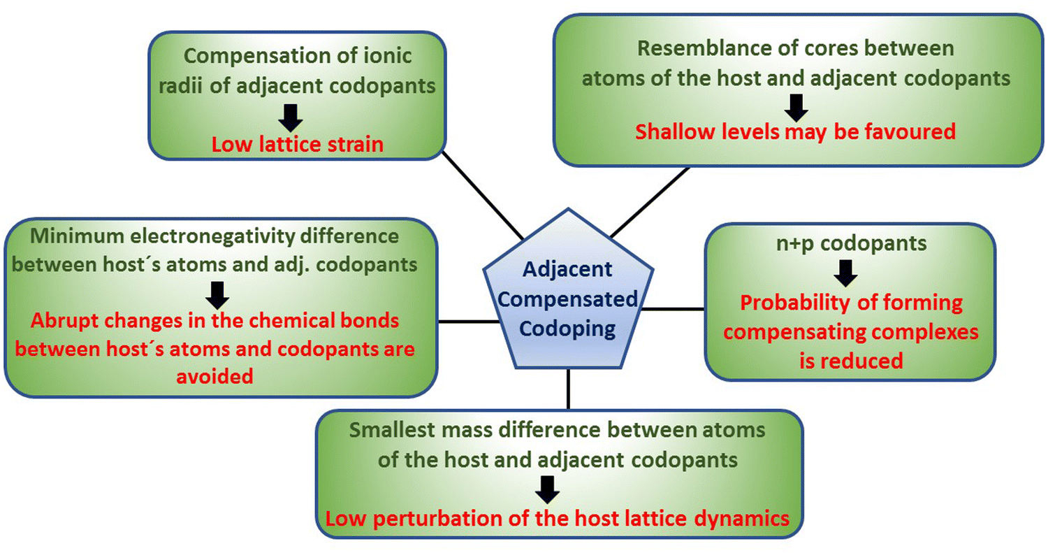
With adjacent compensated codopants,
(a) The strain in the host crystalline lattice is low. In general, the lattice expands owing to the incorporation of ZA,B + 1 impurities, while it contracts upon the incorporation of ZB,A − 1 impurities. This produces a partial, or nearly full, strain balance in the host lattice depending on the ionic radii of the involved adjacent codopants. These combinations substantially reduce dopant solubility issues owing to lattice strain.
(b) The use of n- and p-type impurities reduces the probability of forming compensating defects/complexes, which occur above a threshold concentration in semiconductors with a single type of impurity. It is expected that the presence of acceptors and donors in a certain region of a semiconductor reduces the charge imbalance generated when a single type of dopant is used, which in turn may improve the tunability of the Fermi level.
(c) Adjacent codopants may favor the formation of shallow levels (or bands). Since the atomic cores of adjacent codopants are similar to those of the host's atoms, the levels introduced in the gap by these impurities tend to be shallow. It should be pointed out, however, that this is a rule of thumb when a single type of dopant is used.26
(d) The nature of the chemical bonds (covalent, polar covalent or ionic) in the host shall not change abruptly after the incorporation of adjacent codopants. The electronegativities of the atoms play an important role in the type of chemical bond that binds them. Using adjacent codopants implies that the electronegativity difference between codopants and the host atoms is the smallest possible.
(e) The lattice dynamics of the host are modified to a minimum with adjacent codopants. Since the atomic masses of the adjacent codopants are slightly different from the masses of the host (if adjacent codopants Z ± 1 are employed, the mass differences are the least possible; if the codopants are Z ± 2, the mass differences are the second least possible), the lattice vibrational properties of the host are slightly modified. Under this scheme, any trend toward phonon-related localization effects is poorly favoured (such as polaron localization).
Thus, in ACC, it is sought to maintain the minimum amount of disorder introduced in the host (i.e. low entropy changes owing to strain, local charge unbalance, chemical bonds, mass differences, and phonon frequencies) by the incorporation of two different types of impurities. This is graphically summarized in Fig. 1. The advantages and limitations of ACC are discussed below by presenting actual examples of applying ACC to technologically important semiconductor films, such as CdTe and CdS. Solubility issues were absent in these examples of the employed concentrations of adjacent codopants. Large free electron/hole densities were feasible, implying improved Fermi level tuning capabilities. In some instances, the photoconductivity and transient photo response reached large efficiencies. The results reported here indicate that adjacent compensated codoping can be an alternative paradigm for mitigating the issue of controlling the optoelectronic properties of semiconductors, where single doping faces difficulties. The results below show that in the case of ACC-CdTe, large n-type carrier densities and photoconductivity can be achieved. Additionally, the well-known photoconducting properties of CdS were enhanced. These properties are relevant to solar cell technology.
 | ||
| Fig. 1 Diagram describing the expected effects of applying the adjacent compensated codoping (ACC) concept on semiconductors. For example, in the case of a binary compound AB formed using chemical elements with atomic numbers ZA and ZB, ACC implies codoping with combinations of elements with atomic numbers ZA ± i and ZB ± j, for i, j = 1, 2. | ||
In the examples below, the amounts of codopants introduced in the hosts were in the range of atomic percentages, which produced semiconductors that could be classified as alloys rather than codoped semiconductors. In the case of transparent conducting oxides, such as ITO and FTO, the doping of indium oxide and tin oxide matrices is in the range of atomic percentages, falling rather into the category of alloys. However, the emphasis in this work is on the incorporation of two different dopants, for which the term codoping has been coined in the literature with a specific meaning. In this sense, the difference between alloys and doped semiconductors in this study is irrelevant.
2. Results and discussion
Given its relevance in the search for higher efficiencies in commercial solar cell technology, cadmium telluride was selected as the archetype to investigate the effects of applying the adjacent compensated codoping concept and its feasibility for controlling electrical and photoelectronic properties. A thorough investigation was carried out on two pairs of adjacent codopants in CdTe. Additionally, relevant results on using adjacent codopants in CdS are presented. All materials in this work were prepared in the form of thin films deposited on glass substrates by radio frequency sputtering.2.1 Adjacent compensated codoping applied to cadmium telluride
CdTe is one of the most well-established materials as a photon absorber because of its chemical stability, high absorption coefficient (∼104 cm−1) and band gap (1.5 eV), which almost coincides with the optimal value according to the Shockley–Queisser model.27,28 Efficient doping of CdTe presents some difficulties, especially when p-type conductivity is sought since free hole densities larger than 1015 cm−3 are difficult to obtain.29 In addition, solubility problems have been reported through the formation of secondary phases or metallic segregation.30,31Fig. 2 shows part of the periodic table, where two possible combinations of adjacent compensated codopants for CdTe are indicated. Moreover, Ag + I and In + Sb are the possible combinations of Z ± 1 adjacent compensated codopants. The combination Z ± 2 is not possible for CdTe because it involves Xe, a noble gas. For comparison and clarity purposes, the results for CdTe and CdTe:Ag films are presented first; then, a more detailed characterization of CdTe:(Ag + I) is provided where, strikingly, the secondary phases and Ag clusters observed in CdTe:Ag are avoided through the incorporation of (Ag + I) into CdTe. | ||
| Fig. 2 Part of the periodic table, showing the (Z ± 1) adjacent codopants for CdTe under the adjacent compensated codoping paradigm. CdTe:(Ag + I) and CdTe:(In + Sb) are the resulting materials. | ||
 | ||
| Fig. 3 Structural, morphological, optical and lattice vibrational properties of undoped CdTe films grown at substrate temperatures in the 250–300 °C range. (a) X-ray diffraction patterns showing preferential growth of the cubic (111)/hexagonal (002) planes. To enhance the low intensity peaks, the square root of the intensity was plotted. The broad features between 38° and 50° correspond to convoluted cubic and hexagonal peaks with some amorphous backgrounds. (b) SEM image showing the surface morphology of the film grown at 275 °C. The white bar corresponds to 1 μm. (c) Optical transmittance in the Vis-NIR range showing an abrupt transmission edge for all the films. The oscillations are due to multiple reflections and interferences from the air/film and film/substrate interfaces. (d) Room temperature Raman scattering spectra showing the longitudinal optic mode (LO) of CdTe up to the fifth overtone. | ||
 | ||
| Fig. 4 (a) X-ray diffraction patterns of CdTe:Ag films for silver concentrations of 0.5 and 3 at%. With 3 at%, the solubility limit of Ag in CdTe was surpassed, producing aggregates of Ag and Ag2Te. (b) SEM surface micrograph of the sample with 3 at% Ag, where crystallites as large as one micron were observed (scale bar = 1 micron). (c) Vis-NIR transmittance spectra showing important differences produced by the large absorption coefficient of Ag2Te, which dominates the spectrum of the film with 3 at% Ag. (d) LO mode of CdTe and its overtones observable in the Raman spectra. Raman signal of the Ag2Te aggregates is weak and overshadowed by that of CdTe. | ||
 | ||
| Fig. 5 (a) X-ray diffraction patterns of the CdTe:(Ag + I) films, with the indicated concentrations of adjacent codopants. Secondary phases were not detected as in the case of CdTe:Ag. The panes at the bottom correspond to the powder diffraction data for the cubic (PDF#00-015-0770) and hexagonal (PDF#00-019-0193) phases. (b) Lattice parameter variation in the cubic (a) and hexagonal (c/a ratio) phases as a function of the adjacent codopant concentrations. The parameters were obtained through Rietveld refinements of the diffractograms. (c) Vis-NIR transmittance of the films; the spectra were displaced vertically by the indicated quantities for clarity. (d)–(g) SEM images of the films with 4, 5, 6 and 7 at% AgI in the target. The white scale bar corresponds to 100 nm. | ||
Nonetheless, the influence of the adjacent codopants on the growth habits of the films was noticeable. Fig. 5d–g and Fig. S2 (ESI†) (different magnifications) present the SEM images of the surfaces of the films grown from targets with 4–7 at% AgI. The microstructure changed with respect to undoped CdTe (Fig. 3b) upon increasing the concentration of the codopants. It is pointed out that the 5 at% AgI film showed the largest and best-defined grains, which was consistent with its large photoconductivity, as described below.
Photoluminescence (PL) is a useful technique for studying the electronic properties of semiconductors. In particular, PL has been applied to the study of diverse types of defects, including impurities and complexes in CdTe.44–47Fig. 6a shows the PL spectra of the films obtained at 80 K. All samples were excited using the same laser power density and integration times. The sample with 6 at% AgI presented the most intense signal. The spectrum of CdTe showed a broad band centered at 1.43 eV with two satellite emissions on the sides (Fig. 6b). This spectrum was similar to the one observed in sputtered films grown at 270 °C (nearly the same substrate temperature used in this work, 275 °C) reported by Roland et al., who associated the PL bands with structural defects.45 The energies of the defect levels in the CdTe films are shown in the deconvoluted spectrum in Fig. 6b. The highest energy band occurred at 1.48 eV. The band gap of CdTe at 80 K is reported experimentally at 1.595 eV.48 The excitonic transition in Fig. 6b was absent even though its binding energy (11.7 meV49) was above the thermal energy during the measurements (kBT = 6.89 meV). This indicates that exciton recombination can be mediated, or inhibited, by defect levels. Based on Roland et al.'s work, a CdCl2 treatment was necessary to produce a weak feature identified as excitonic. Except for the film with 6 at%, the spectra of the CdTe:(Ag + I) films shifted to higher energies with common maxima at 1.51 eV. The emissions of the codoped films were broad and asymmetric, with different relative intensities. The asymmetry was the result of three different emissions, as shown in the deconvoluted spectrum of the 5 at% sample in Fig. 6c. It is interesting to note that, even though in the literature there are no reports on the PL of CdTe:(Ag + I), the emissions at 1.45, 1.47 and 1.51 eV have their counterparts in CdTe doped with chlorine,50 an isovalent element with iodine. In this case, the band at 1.45 eV was associated with A centers, which are complexes formed by Cd vacancies and ClTe donors. The band at 1.47 eV was identified as D–A recombinations.50 In another work, the same band was linked to structural extended defects.45 Although close in energy to the double-peak (DP) band at 1.55 eV,45 the origin of the band at 1.51 eV (80 K) has not been identified. Previous studies in CdTe:I films showed that the PL intensity can be 10–100 times stronger than in bulk CdTe.47,51 Some enhancement with respect to CdTe (∼5 fold) was observed for the sample with 6 at% (Ag + I), Fig. 6a. In the case of silver, it is a shallow impurity in CdTe for which near-edge emissions at 1.588 eV were observed at 1.8 K.52 Considering that the band gap of CdTe at that temperature is 1.606 eV, the ionization energy of the Ag level is ∼18 meV, which makes it unlikely that the 1.51 eV emission in CdTe:(Ag + I) is related to silver since the activation energy is E80Kg − 1.51 eV = 85 meV. The similarities between the PL spectra of CdTe:(Ag + I)-5 at% and CdTe:Cl suggest analogous defect-passivation effects produced by the isovalent halide iodine (in CdTe:(Ag + I)) and chlorine (in CdTe:Cl), which in turn produce comparable defect-related radiative transitions.
 | ||
| Fig. 6 (a) Photoluminescence spectra of CdTe and CdTe:(Ag + I) films measured at 80 K using a 785 nm laser as the excitation source. All samples were excited using the same laser power density and integration times. (b) Deconvolution of the PL spectrum of the undoped CdTe and (c) the film with 5 at% AgI. (d) Chemical composition of the CdTe:(Ag + I) films obtained using WDS as a function of the concentration of AgI in the sputtering target. | ||
The electrical properties of CdTe were significantly enhanced upon the incorporation of the adjacent codopants Ag + I. The results of the room temperature Hall effect measurements for concentrations between 4 and 7 at% are presented in Fig. 7a. The films with concentrations below 4 at% had resistivities larger than the equipment limit (∼107 Ω cm). The resistivity of the codoped CdTe:(Ag + I) films dropped monotonically with the (Ag + I) concentration. The resistivity of the film with 7 at% was 36 Ω cm, 6 orders of magnitude lower than that of intrinsic CdTe, whose resistivity is typically ∼107 Ω cm. The mobility, however, decreased, obtaining values between 6.5 and 0.2 cm2 V−1 s−1 as the concentration of codopants changed from 4 to 7 at%. As opposed to undoped CdTe, the codoped films presented n-type characteristics, with free electron densities varying from 1015 to ∼1 × 1018 cm−3.
 | ||
| Fig. 7 (a) Values of the free electron concentration, mobility and resistivity obtained at room temperature Hall effect of the n-type CdTe:(Ag + I) films as a function of the concentrations of codopants. (b) Generic energy diagram of a semiconductor with adjacent compensated codopants illustrating, for example, the formation of donor- and acceptor-like sub-bands with ionization energies En and Ep, widths δEn and δEp, and densities of states Dn and Dp. The Gaussian-like shape of the densities of states was arbitrary to depict a possible non-uniform inter level spacing. The position of the Fermi level (violet arrow) is a function of the concentration of adjacent codopants, the position and characteristics of the donor/acceptor sub-bands and their occupancy. | ||
The compound AgI was used in the target as a source of silver (acceptor) and iodine (donor). These two elements were thus present in the target in a one-to-one ratio. However, the films were not highly resistant when full compensation occurred. Two observations can be made in this regard. First, the concentration of adjacent codopants in the target was not replicated in the films. This is a consequence of the different properties of the compounds, such as sputtering yield, sticking coefficients, and the natural off-stoichiometric trend of each compound. For example, CdTe tends to be Cd deficient owing to the large vapor pressure of this element. Fig. 6d shows the chemical composition of the CdTe:(Ag + I) films obtained by WDS, where it is noticed that the [Te]/[Cd] and [Ag]/[I] ratios are larger than one. Since the concentrations of adjacent codopants are of the order of atomic percent, it is expected that the impurity levels form sub-bands rather than discrete spaced apart levels. Second, the donor- and acceptor-like sub-bands, in general, present several asymmetries, as depicted in Fig. 7b. In particular, these are characterized by different ionization energies En and Ep, different widths δEn and δEp, and different densities of states Dn and Dp since the inter-level separation in the sub-bands is not necessarily the same (the surroundings of each impurity in the lattice is different). The characteristics of the donor and acceptor sub-bands (Ei, δEi and Di) and their electronic occupation determine the type and magnitude of the conductivity. Another factor that should be considered is the substitutional or interstitial incorporation of the adjacent codopants in the CdTe lattice. Their location in the lattice can generate p- (AgCd, Ii, and VCd) or n-type (Agi, ITe, and VTe) conductivity. However, it is expected that the similarities between the adjacent codopants and the atoms of the host favor substitutional incorporations (AgCd and ITe). Besides, the donor and acceptor sub-bands with separate impurity levels are not ruled out, which could be the result of codopants at non-substitutional sites, forming complexes with defects or with the host's atoms.
Photoconductivity (PC) was one of the most improved properties of CdTe when the ACC approach was applied. The photoconductivity of a semiconductor is an important property since it can be applied in various optoelectronic devices, such as photo detectors, sensors and solar cells. The enhancement of the electrical conductivity in a semiconductor under illumination is due to the photo-generation of electron–hole pairs, which produce electrical current when an electric field is applied. It is shown below that ACC transformed the sputtered CdTe films from having negligible photoconducting activity to a photo current three orders of magnitude larger than the current in the dark. PC was investigated under two conditions: steady state and transient (on–off) illumination.
In a semiconductor characterized by electron and hole concentrations at equilibrium n0 and p0 and drift mobilities μn and μp, under illumination, the increase in conductivity is given by53
| σph = Δσ = σlight − σdark = e (μnΔn + μpΔp), |
 | ||
| Fig. 8 (a) Current–voltage characteristics of a CdTe-sputtered film under illumination and in the dark. In both cases, the current was at the level of noise (<nA). (b) Photosensitivity (r = ILight/IDark) of the CdTe:(Ag + I) films as a function of the concentration of AgI in the target. The largest value of r (5.15 × 10³) was obtained for the film with 5 at%. (c) Comparison of the photocurrent in the light and in the dark as a function of applied voltage for the film with 5 at% AgI in linear and semi logarithmic graphs. The photocurrent was three orders of magnitude larger than that in the dark. The ohmic characteristics of the CuTe contacts are appreciated in the linear graph. (d) Transient photoconductivity of the films with 4–6 at% AgI for an applied voltage of 1 V. (e) Work function of the CdTe and CdTe:(Ag + I) films obtained using Kelvin probe force microscopy for the indicated concentrations of AgI in the sputtering target (scanned surface: 1 × 8 μm2). | ||
Transient photoconductivity (TPC) is a property useful for analyzing the response of a semiconductor to light on/off cycles. The TPC data for films with 4–6 at% AgI are shown in Fig. 8d. The photocurrent presented sharp on/off steps, with different values of the saturation current (light-on plateaus) and the currents in the dark. The largest on/off current contrast was for the film with 5 at% AgI, as expected from the photosensitivity data in Fig. 8b. The largest photocurrents were ∼0.145 μA for the films with 5 and 6 at%. The electrical contacts were stable during the on/off cycles, allowing for the efficient transfer of the carriers. A slight decrease in the photocurrent during the TPC cycles with time was observed in the sample with 6 at% AgI (Fig. 8d). This reduction has been ascribed to a drop in the free electron density in other II–VI semiconductors, such as CdS and CdSe.57 Importantly, the incorporation of the adjacent codopants Ag + I reduced the work function (W) from 5.6 eV for undoped CdTe to values between 4.52 and 4.75 eV, as shown in Fig. 8e. Thus, the Fermi level was a function of the concentration of Ag + I. This result is relevant for applications in which obtaining ohmic contact with CdTe has been challenging because of its large work function. Several approaches have been undertaken in photovoltaic devices to overcome this problem, sometimes resulting in complicated structures or technical difficulties. Considering that the work function of CuTe (the material of the contacts in the PC experiments) is 4.85 eV58 and from the values in Fig. 8e, the work function difference (ΔW) at the CuTe/CdTe junction is 0.75 eV, which contrasts with ΔW = 0.15 eV for the CuTe/CdTe:(Ag + I)-5% interface, an important 0.6 eV reduction at the interfacial barrier.
 | ||
| Fig. 9 (a) X-ray diffraction patterns of the CdTe:(In + Sb) films for the indicated codopant concentrations. (b) and (c) SEM surface micrographs of the samples with 4 and 7 at% InSb, respectively; the white bar corresponds to 100 nm. (d) Vis-NIR spectra of the codoped films in the 400–1400 nm range. (e) Chemical composition of the CdTe:(In + Sb) films obtained using WDS as a function of the concentration of InSb in the sputtering target. | ||
Contrary to the case of CdTe:(Ag + I), the electrical conductivity of CdTe:(In + Sb) did not improve. Indeed, the resistivity of the CdTe:(In + Sb) films was large for all codopant concentrations beyond the measurement capabilities of the employed Hall-effect system (∼107 Ω cm). Such large resistivities can be associated with the small grain size and large density of defects in these samples, as observed in the SEM images (Fig. 9b, c and Fig. S3c, d, ESI†). The average grain size in CdTe:(In + Sb) was reduced roughly 2.5 times with respect to that of undoped CdTe (∼120 vs. 300 nm). These results show that neither In nor Sb produces recrystallization and defect passivation as halides do in CdTe. In the Vis-NIR spectra shown in Fig. 9d, it can be observed that the abruptness of the optical transmittance edge was maintained in the codoped films and that the average transmittance for energies below the band gap was around 70%, as in the case of undoped CdTe films. Fig. 9e shows the chemical composition of the films obtained by WDS. Indium incorporated more readily than Sb, while the concentrations of Cd and Te were nearly the same.
2.2 Terahertz spectroscopy
The results presented above show that for the substrate temperature of 275 °C, the electrical conductivity of CdTe was improved by five orders of magnitude if the adjacent codopants Ag + I were incorporated. Nonetheless, when the other pair of adjacent codopants In + Sb was used, the resistivity of the films remained high. In CdTe:(Ag + I), the photocurrent was largest when the concentration of adjacent codopants was 5 at%. This concentration was selected for further studies on the physical differences between CdTe:(Ag + I) and CdTe:(In + Sb). To this end, electronic levels inside the band gap were probed through attenuated total reflectance spectroscopy (ATR) using a Fourier-transformed terahertz spectrometer. Fig. 10 shows the absorbance spectra of CdTe, CdTe:(Ag + I)-5% and CdTe:(In + Sb)-5%. In the wavenumber region between 70 and 280 cm−1 (Fig. 10a), the spectra of the three samples exhibited the TO and LO modes of CdTe at 142 and 169 cm−1, respectively.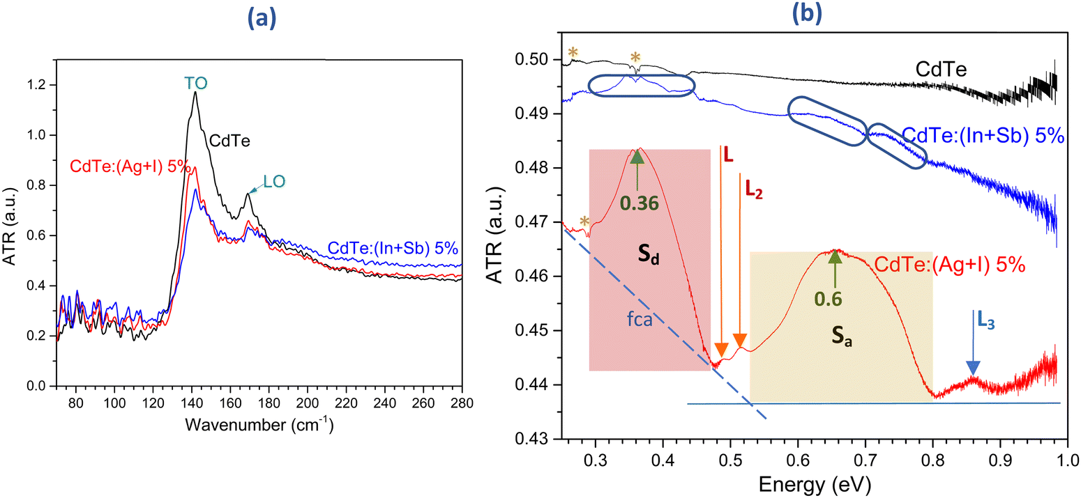 | ||
| Fig. 10 Room temperature attenuated total reflection (ATR) terahertz spectroscopy absorbance measurements of CdTe, CdTe:(Ag + I)-5% and CdTe:(In + Sb)-5% films. (a) Transverse optical (TO) and longitudinal optical (LO) phonons of CdTe are observed at 142 and 169 cm−1, respectively. (b) ATR spectra from 0.25 eV (2000 cm−1) to 0.98 eV (7900 cm−1). The spectrum of undoped CdTe did not present any clear absorption features. The spectrum of CdTe:(In + Sb) showed weak bands, denoted by the blue elongated shapes. Two well-defined absorption bands centered at 0.36 eV (Sd) and 0.66 eV (Sa) appeared in the spectrum of CdTe:(Ag + I). The widths of these bands were different (highlighted in the figure). The absorption due to free carriers is indicated by the blue dashed line labeled as fca. The appearance of the bands Sd and Sa correlated with the lower resistivity of the CdTe:(Ag + I)-5% films (750 Ω cm, Fig. 7a). The samples of CdTe and CdTe:(In + Sb)-5% were highly resistive (ρ > 107 Ω cm). The small sharp features in the spectra (denoted with asterisks) are remnants of the subtraction of the substrate signal. | ||
The ATR spectra ranging from 0.25 to 0.98 eV are shown in Fig. 10b. It is observed that the spectrum of pristine CdTe did not present absorption bands in this interval. The small features labeled with asterisks in the three spectra are residues from the subtraction of the substrate (glass) spectrum. The spectrum of CdTe:(Ag + I)-5% was strikingly different since two broad, well-defined absorbance bands developed with their maxima at 0.36 eV (Sd) and 0.66 eV (Sa). Furthermore, three weak features L1 (0.49 eV), L2 (0.52 eV) and L3 (0.86 eV) were evident. Free carrier absorption has been reported in CdTe bulk and films,66–69 where, depending on the free carrier concentrations, the onset of the absorption occurred at wavelengths between 1.4 and 2.8 μm (0.44–0.88 eV). The onset of the free carrier absorption (fca), the blue dashed line depicted in Fig. 10b, occurred at 0.54 eV. A discussion of possible energy diagrams compatible with the ATR spectrum of CdTe:(Ag + I)-5% is presented in the ESI† (Fig. S4 and S5). From that analysis, the energy diagram shown in Fig. 11 is proposed to describe the electronic transitions observed in the absorbance spectrum of CdTe:(Ag + I)-5% illustrated in Fig. 10b.
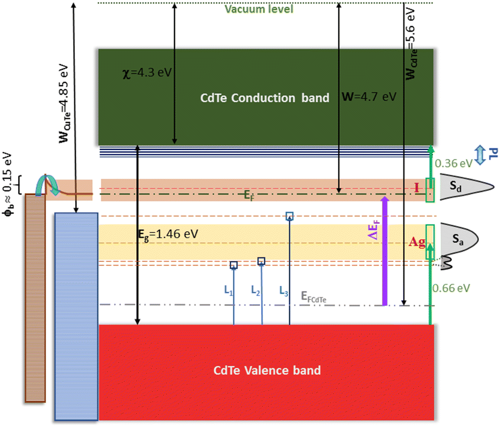 | ||
| Fig. 11 Proposed energy diagram for the ATR absorbance spectrum of the film CdTe:(Ag + I)-5 at% in Fig. 10b. The reported electron affinity of CdTe (4.3 eV) and the work function of the sample measured using Kelvin probe force microscopy (4.7 eV) in Fig. 8e were considered. The Fermi level (gray dash–dot–dot line) and work function of pristine CdTe (5.6 eV, Fig. 8e) are shown as references. The change in the Fermi level from undoped p-type CdTe to n-type CdTe:(Ag + I)-5% was ΔEF = 0.9 eV, as indicated by the purple arrow. The prominent absorbance features in Fig. 10b are depicted on the right-hand side. As shown in Fig. 10b, the width of Sa was ∼0.27 eV and that of Sd was ∼0.19 eV. Transitions Li in the figure are tentative, considering that the excited electrons depart from the valence band. The energy diagram for the electrical contacts with CuTe (used for the Hall effect and photoconductivity measurements) is represented on the left-hand side with brown symbols. The work function of CuTe is 4.85 eV.55 A barrier of 0.15 eV at the film/contact interface yielded contacts with ohmic characteristics, as shown in Fig. 8c. | ||
2.3 Donor/acceptor sub-bands and intermediate band solar cells
In the diagram in Fig. 11, the position of the Fermi level (EF) near the bottom of the donor sub-band Sd implies that most of the levels in this sub-band are empty, and a lower number below EF is occupied. The empty levels were created when the extra electrons of the donors (iodine) in Sd transitioned to the acceptor (silver) sub-band Sa, that is, the acceptor sub-band was occupied by electrons from the donor sub-band to achieve a lower energy state. Electronic transitions from the valence band (VB) to the acceptor sub-band, 0.66 eV apart, are negligible for thermal excitations or quantum tunneling. A partially empty donor sub-band was possible because compensating impurities were employed, and because the acceptor sub-band Sa was deep (to avoid its occupancy by thermally excited electrons from the VB). Other scenarios regarding deep and shallow sub-bands are discussed below. If donors and acceptors were in a one-to-one ratio, for each extra electron in the donor sub-band, there is a hole in the acceptor sub-band. In this case, the acceptor sub-band is totally occupied by electrons from the donor sub-band, which is empty or partially empty if statistical fluctuations are considered. An empty sub-band could be utilized for electron transport provided contacts with appropriate work functions were used. In other words, the ACC paradigm can be used to generate intermediate bands as it has been conceptualized for high efficiency intermediate-band solar cells. In this case, electrons can be photo excited to the conduction band (CB) in a single transition or through two-step excitations involving lower energy photons. As depicted in Fig. 11, the donor sub-band can be utilized by photo excited electrons with energies lower than Eg. Electronic transitions of types VB → Sd → CB and Sa → Sd → CB are possible. Besides arriving at the CB, the photo excited carriers must reach the contacts for their extraction to an external circuit. This requires that the lifetimes of the photo generated electron–hole pairs be long enough to enable them to reach the contacts. In CdTe:(Ag + I), this was demonstrated through photoconductivity experiments. As mentioned, the photo current was particularly high (>5000 times larger than the current in the dark) for the films with 5 at% AgI (Fig. 8b), a result that could be associated with defect passivation by Ag + I, in analogy with the activation treatments of CdTe with chlorine.Two features distinguish the electron states in the sub-bands from the extended states in the conduction and valence bands. First, codopants do not form a periodic sublattice since they occupy non-periodic (random) sites in the host. Thus, the sub-band states cannot be described through Bloch functions, which implies a certain degree of localization. The second aspect arises from the fact that the concentration of codopants was two orders of magnitude lower than the atomic density of the host, which means that the densities of states in the sub-bands are roughly lower by the same factor. The formation of states in the band gap due to complexes cannot be ruled out.
In the ATR and photoconductivity experiments, the sample was exposed to light from IR or tungsten-halogen lamps, respectively, as sources of photons that produced electronic transitions, such as VB → CB, VB → Sd, Sa → Sd, Sa → CB, and Sd → CB. In the photoconductivity experiments, a small barrier (∼0.15 eV) was formed between the film and the CuTe contact (Fig. 11), which is consistent with the measured ohmic behavior shown in Fig. 8c. Upon illumination, electrons were continuously excited to the CB from VB, Sa or Sd. The close match between WCuTe and EF of CdTe:(Ag + I)-5% permitted electron transport through the sub-band Sd in addition to the electrons traveling in the extended states of the CB. The weak absorbance features L1, L2 and L3 illustrated in Fig. 10b were represented tentatively in Fig. 11 as electronic transitions from the VB to levels produced by intrinsic or extrinsic defects. The states detected by photoluminescence (Fig. 6c) and by Hall effect experiments as a function of temperature (activation energies) (Fig. S6, ESI†) are depicted in Fig. 11 close to the CB edge.
The ATR spectrum of the CdTe:(In + Sb) films did not present well-defined absorbance bands. Instead, the spectrum consisted of a slanted base line and weak absorbance features denoted by the blue elongated shapes shown in Fig. 10b. It is not clear why absorption bands were observed in the ATR spectra of CdTe:(Ag + I) 5 at% films but not for CdTe:(In + Sb) 5 at%. In addition to defects, such as dislocations, vacancies, antisites and interstitials, a large number of surface recombination centers is expected in the CdTe:(In + Sb) films owing to their small grain size (Fig. 9b and c). In fact, the large resistivity of these samples can be ascribed to their large defect density and small grain size. It is noteworthy that the high resistivity was not reduced in the films grown at 400 °C, even though it was the temperature at which In and Sb were incorporated completely into the CdTe lattice according to the Raman spectroscopy data depicted in Fig. S3b (ESI†). However, in the CdTe:(Ag + I) films, defect passivation through recrystallization played a role in their noted electrical and photoelectronic properties in analogy to the effects of treatments with chlorine.
2.4 Adjacent compensated codoping applied to CdS:(Ag + Cl)
To investigate further the applicability of ACC, cadmium sulfide films were grown by incorporating the adjacent codopants chlorine and silver. CdS is a II–VI semiconductor widely employed as a window or buffer layer in solar cell technologies, such as those based on CdTe, CuInSe2, Cu2ZnSnS4, and hybrid perovskites. Besides analyzing the structural, electronic, lattice dynamics and optical properties of codoped CdS, this material was selected to investigate the effect of adjacent codopants in its intrinsic photoconductivity since CdS is a well-known photoconductor.70–72 It is shown below that, indeed, ACC improves this capacity of CdS.CdS thin films were deposited on glass substrates at 250 °C. In this case, the selected adjacent codopants were silver and chlorine, as illustrated in Fig. 12. Silver chloride (AgCl) was used as the source of these elements in the fabrication of the sputtering targets. Other possible adjacent codopants for CdS are In + P, for which the compound InP is the natural source. However, preference was given to AgCl because of its lower cost. Films of CdS:(Ag + Cl) were grown with the following AgCl concentrations in the targets: 0.5, 1.0, 2.0, 3.0, 4.0 and 5 at%. These concentrations refer to the [Ag]/[Cd] ratios. The thicknesses of the samples varied between 76 and 110 nm (Table S3, ESI†).
 | ||
| Fig. 12 Portion of the periodic table illustrating chlorine and silver as adjacent compensated codopants for cadmium sulfide (CdS). To incorporate these elements into CdS, silver chloride (AgCl) powder was used in the fabrication of the sputtering targets. | ||
Fig. 13a shows the X-ray diffraction patterns of the codoped films and pristine CdS. Only the undoped film presented a mixture of cubic and hexagonal phases. In the codoped samples, the crystalline structure was hexagonal (wurtzite type), as identified by the powder reference card PDF#00-006-0314. Diffraction peaks different from those of CdS were absent for codopant concentrations lower than 4 at%. In the patterns of the films with 4 and 5 at% AgCl, a small peak at 38° was identified as being related to Ag aggregates. It is not ruled out, however, that a complete incorporation of silver into the CdS lattice can be obtained at higher substrate temperatures, as occurred in the case of InSb and CdTe (see above).
 | ||
| Fig. 13 (a) X-ray diffraction patterns of the CdS and CdS:(Ag + Cl) films. As a reference, the powder diffraction cards for CdS illustrating hexagonal (PDF#00-006-0314) and cubic (PDF#00-010-0454) symmetry are shown at the bottom. (b) Room temperature Raman spectra of undoped and codoped films. (c) UV-Vis-NIR transmittance spectra. (d) Chemical composition of the sputtered films obtained using WDS as a function of the nominal concentration of AgCl in the sputtering target. | ||
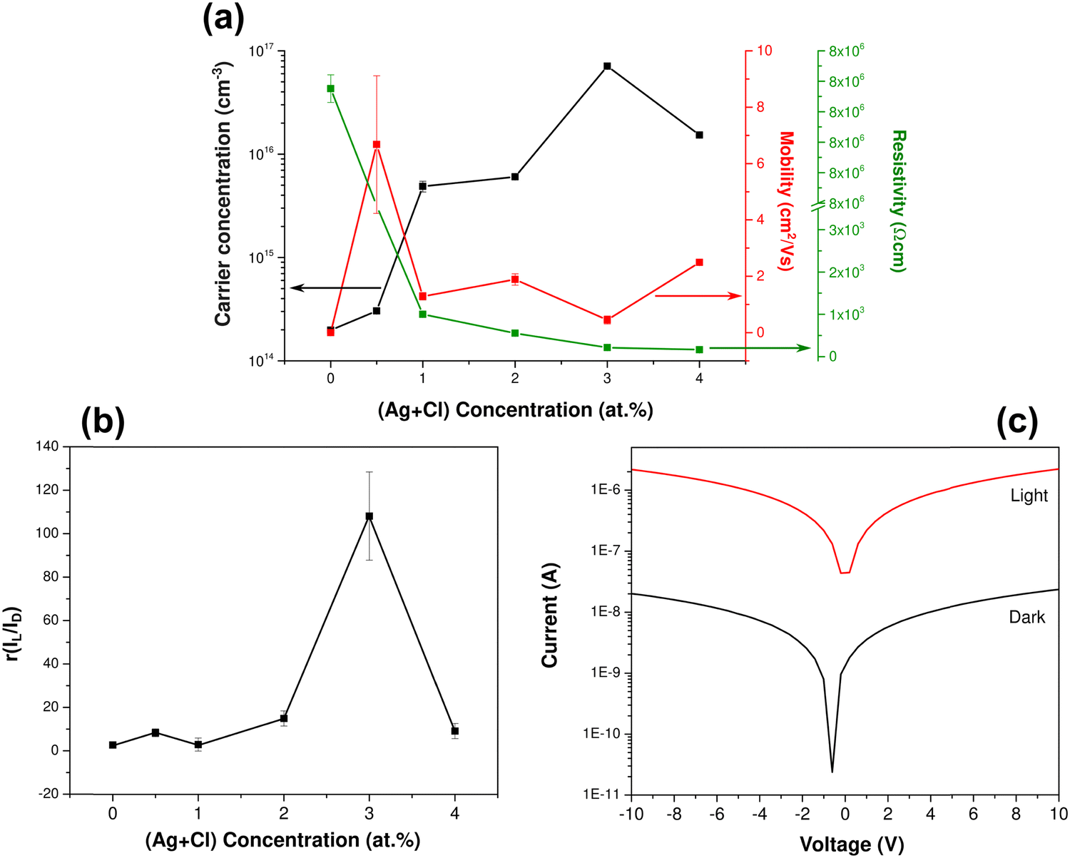
The lattice parameter c of the hexagonal structure was determined from the X-ray diffractograms through Rietveld refinements using Fullprof.43 The values of this parameter for undoped CdS and codoped CdS:(Ag + Cl) films are shown in Fig. S7a (ESI†) for the different concentrations of adjacent codopants. The strain (S = Δc/c0, where c0 is the lattice constant of the undoped film) induced by Ag + Cl was determined, which is lower than 0.2% for all films. Analogously, the change in the c/b ratio was lower than 0.5% (Fig. S7b, ESI†). The interatomic distances of CdS were hardly modified by the adjacent compensated codopants. The ionic radii of the Cd2+ and Ag1+ cations for coordination four are 78 and 100 pm, respectively. The radii of four-fold coordinated anions S2− and Cl1− are not known; however, as mentioned above, it is expected that their values maintain approximately the similarity that these elements exhibit for six-fold coordination, whose radii are 184 and 181 pm, respectively.42Fig. 13b illustrates the room temperature Raman spectra of the films. Owing to the similar atomic masses of silver and chlorine with respect to cadmium and sulfur, respectively, the frequency and shape of the CdS Raman modes were basically unaltered. The transmittance spectra of the films are presented in Fig. 13c. It is noticed that the absorption edge is more abrupt for the 3 at% Ag + Cl film, indicating a lower number of defect levels close to the band edges. Accordingly, this sample presented the best photoconductivity performance (see below). The band gap was estimated from Tauc's plots. It varied monotonically with codopant concentration from 2.36 eV for undoped CdS to 2.18 eV for the film with 4 at% AgCl (Fig. S8, ESI†). Fig. 13d shows the chemical composition of the films obtained by WDS as a function of the nominal concentration of AgCl in the sputtering targets. The concentrations of Ag and Cl in the targets were replicated closely in the films. The contents of S and Cd decreased correspondingly when the dopant concentration rose.
Room temperature Hall effect measurements were carried out using silver for the contacts (Fig. 14a). In general, the incorporation of Ag + Cl improved the electrical properties of CdS, whose n-type characteristics remained unchanged. The resistivity decreased from 8.2 × 10⁶ for CdS to 163 Ω cm for the CdS:(Ag + Cl)-4% film, that is, a reduction of four orders of magnitude. The free charge carrier density increased from 2 × 10¹⁴ in CdS up to 7 × 1016 cm−3 for the sample with 3 at% AgCl. The average mobility of the film with 0.5 at% Ag + Cl was 6.7 cm2 V−1 s−1, an enhancement of three orders of magnitude with respect to that of undoped CdS, which had a value of 0.005 cm2 V−1 s−1. The electrical parameters of the film with 5 at% Ag + Cl could not be obtained reliably owing to contact issues.
 | ||
| Fig. 14 (a) Room temperature electrical parameters of CdS and CdS:(Ag + Cl) films obtained through Hall effect measurements as a function of the concentration of adjacent codopants. (b) Photosensitivity (r = ILight/IDark) of the films. (c) Comparison of the photocurrent and current in the dark as a function of the applied voltage for the film with 3 at% AgCl. The photocurrent was two orders of magnitude larger than the one in the dark for this film. | ||
CdS is a well-known photoconductor.69–71 It was considered convenient to test the effect of ACC on this natural property of CdS. The photosensitivity (r = ILight/IDark) of all the samples is presented in Fig. 14b. For undoped CdS, the photocurrent was four times larger than in the dark (r = 4). Adjacent codopants improved this value since the photosensitivity of all the codoped films was larger than 4. Interestingly, the photosensitivity of the film with 3 at% was r = 115. Fig. 14c shows the photocurrent of this film for applied voltages between −10 and +10 V.
In summary, ACC applied to CdS produced films whose crystalline structure, optical properties and lattice dynamics were affected paltry. The electrical resistivity was reduced by four orders of magnitude, with significant improvements in the free carrier density and mobility. The photosensitivity of CdS was enhanced for all codopant concentrations. The largest improvement (∼102) was obtained for the film with 3 at%. The enhancement of the photoconductivity in CdS presents some analogy with studies of CdTe/CdS solar cells, in which it was found that chlorine decorates CdS grain boundaries and lowers the defect density by promoting recrystallization.73
In the case of CdTe:(Ag + I), the largest photosensitivity was obtained for the films with 5 at% Ag + I. The existence of optimal concentrations of adjacent codopants in the photoconductivity of CdTe and CdS is noteworthy. The reproducibility of these results was verified by measuring the photosensitivity in samples grown with the same parameters in different runs. The incorporation of impurities in the host lattice occurs at random sites. However, the existence of reproducible concentrations, which optimize the photoconductivity, is consistent with spatial distributions of the adjacent codopants, not totally arbitrary. The results indicate that the average distribution of codopants was replicated in the samples. The driving mechanism behind this behavior might be the energy reduction of the host + codopant system. A hypothetical distribution of impurities could simply be an optimal average inter-impurity distance or a more elaborate distribution that could involve codopants, vacancies, or complexes. In either case, the physical phenomena involved in the optimization modulate the photo generation, the transport of the excited electron/hole pairs, and the competing recombination processes. Further studies are required to shed light on the underlying mechanisms of photoconductivity in CdTe and CdS and their dependence on the concentration and spatial distribution of the adjacent codopants. In addition, given the striking differences in results depending on the use of halide co-dopants (I for CdTe and Cl for CdS), further work is required to evaluate the impact of halide inclusion on the properties of the codoped materials, which may have effects analogous to chlorine treatments in CdTe device processing. In this direction, films of CdTe:I-5 at% were deposited at 275 °C (the same concentration and substrate temperature used to grow the best performing CdTe:(Ag + I) films), obtaining highly resistive polycrystalline films (Fig. S9a, ESI†). This indicates that the conductivity of the codoped films results from the combined effect of the adjacent codopants Ag + I. Detailed analyses of the CdTe:I and CdS:Cl systems, varying growth conditions and halide concentrations are necessary to shine light on the role of halides in the codoped films.
2.5 Sub-bands: some possible scenarios
The energy of the acceptor and donor sub-bands relative to the host's conduction and valence band edges strongly influences the electrical and optoelectronic properties of the codoped semiconductors. In the discussion below, a two-sub-band model, as observed in CdTe:(Ag + I) 5 at%, is considered to analyze possible scenarios of the changes introduced by adjacent codopants in the band structure of the host. The formation of more than two sub-bands in different host + codopant systems is not ruled out. However, the consideration of two sub-bands, a donor-like and an acceptor-like, is a natural base for the analysis of more complicated distributions of the impurity levels. Sub-bands Sd and Sa may present different ionization energies (En, Ep), widths (δEn, δEp) and densities of states (Dn, Dp). A good number of combinations can occur when the ACC paradigm is applied to different semiconductors. For example, in one particular material with different pairs of codopants, or for the same host + codopants system grown under different thermodynamical conditions or deposition method.Given the experimental data for CdTe:(Ag + I) gathered so far, the energy diagram depicted in Fig. 11 was devised, indicating not only the existence of the sub-bands Sd and Sa but also of some shallow levels detected by photoluminescence (Fig. 6c) and temperature-dependent Hall effect measurements (Fig. S6, ESI†). Silver and iodine, separately, do not form deep levels in CdTe. The former has an ionization energy of 0.15 eV, while the latter is 0.05 eV.29 The origin of the change from shallow levels to the formation of deep sub-bands, as found in this work, needs to be determined. In what follows, the properties of the sub-bands (En, Ep, δEn and δEp) and their effect on the charge transport processes through direct electronic transitions involving Sd and Sa are discussed. Other mechanisms, such as trapping–detrapping or Auger recombination, are not considered herein. When two sub-bands, Sd and Sa, form, a lower energy state of the crystal is attained when the electrons from the donor atoms occupy the lower energy states in the acceptor sub-band. Physically, this means that the electrons from the donors move around through the lattice until they eventually fill the incomplete bonds of the acceptor atoms.
As a starting point in this analysis, the case when δEn ≈ δEp (similar sub-band widths) is considered. Sub-bands Sd and Sa can be shallow or deep. If the sub-bands are shallow (Fig. 15a), electrons from Sd may access the CB through thermal excitations or quantum tunneling and travel amidst the crystal until recombine with holes in Sa. Analogously, electrons from the VB can transfer to Sa. Both processes may occur until all states in Sa are occupied. Then, additional electronic transitions towards the full sub-band Sa cannot occur, and owing to statistical fluctuations, a low concentration of electrons (n) in the CB and holes (p) in the VB remains (Fig. 15b). If p ≈ n, (nearly) full compensation is obtained owing to band-to-band recombination (black arrows in Fig. 15b). The depleted sub-band Sd could be utilized for electron transport if contacts with appropriate work function were applied.
 | ||
| Fig. 15 Energy diagrams for two sub-bands in the band gap: a donor-like (Sd) and an acceptor-like (Sa) with widths δEn ≈ δEp. (a) Shallow sub-bands. Electrons from Sd can transfer to the CB, followed by transitions to Sa. Thermal excitations and quantum tunneling may promote electrons from the VB to Sa. Electron–hole recombinations Sd → Sa are indicated by the blue dashed arrow. (b) Once Sa is occupied, band-to-band recombination of electrons in the CB (with density n) with holes in the VB (with density p) produces low conductivity for n ≈ p. (c) If the sub-bands are deep, transitions from the VB to Sa and from Sd to the CB are negligible. Electrons in Sd lower their energy by recombining with states in Sa. (d) If the densities of states of the donor and acceptor sub-bands are comparable, most states in Sa will be occupied and those in Sd will be mostly vacant. Statistical fluctuations prevent completely full or empty sub-bands. The green dashed arrows indicate transitions of electrons under illumination for photons with energies Ei ⪝ Eg. The dotted green line indicates the relaxation processes through the emission of phonons. | ||
If the ionization energies for Sd and Sa are large (deep bands), as shown in Fig. 15c, electrons from Sd cannot be thermally excited or tunneled to the CB, or from the VB to Sa. Electrons in Sd lower their energy by recombining with the available states in Sa. This process may continue until Sd is depleted, and the states in Sa are occupied (Fig. 15d). In this situation, several transitions are possible if the material is exposed to a photon flux with energies ⪝Eg, as indicated by the green dashed arrows illustrated in Fig. 15d.
Next, the case of deep sub-bands when δEn ≠ δEp is considered. If δEn < δEp (Fig. 16a), Sa is partially filled, and Sd is depleted. Accessible states in Sa, Sd and the CB can be used for the arrival of photo-excited electrons from Sa or VB, as illustrated by the green dashed arrows in Fig. 16b. The dotted green lines indicate possible relaxation processes through the emission of phonons. If δEn > δEp (Fig. 16c), available states for photoexcited electrons occur in the CB and partially in Sd. The generation of free carriers under illumination is largely assisted when the sub-bands are deep, especially if δEn < δEp (Fig. 16a and b) (more pathways for electronic transitions).
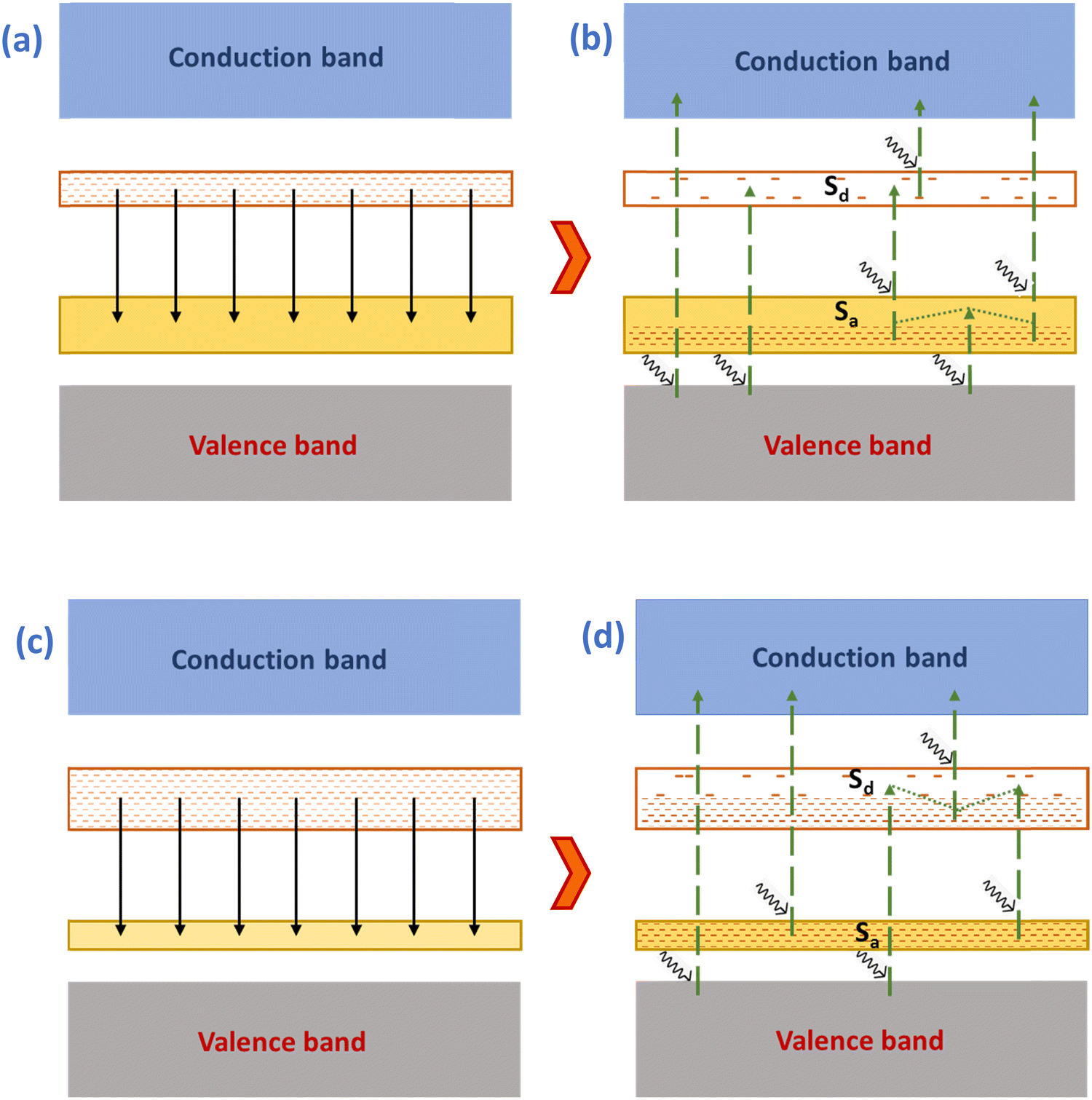 | ||
| Fig. 16 Two possible energy diagrams for the deep donor (Sd) and acceptor (Sa) sub-bands with different widths δEn ≠ δEp. (a) If δEn < δEp, electrons in Sd lower their energy via transitions to Sa. (b) Sa is not fully occupied, while Sd is depleted. (c) If δEn > δEp, electrons in Sd lower their energy through transitions to Sa. (d) If the number of electrons in Sd is larger than the available states in Sa, the former will be partially empty, and the latter will be occupied. The green dashed arrows indicate transitions of electrons under illumination with incident photons, with energies Ei ⪝ Eg. The dotted green lines indicate the relaxation processes through the emission of phonons. | ||
The energy diagrams illustrated in Fig. 15 and 16 describe the distribution of carriers relevant to the electrical and photoelectronic properties of a semiconductor, providing sub-bands Sd and Sa form. The diagram illustrated in Fig. 11 for CdTe:(Ag + I) corresponds to the type depicted in Fig. 16b. In different materials, a different distribution of acceptor and donor levels may occur depending on the type and concentration of codopants and on the thermodynamical conditions during growth. Other combinations of adjacent codopants need to be explored. For instance, those using uncompensated p–p (ZA − 1, ZB − 1 in compound AB) or n–n (ZA + 1, ZB + 1) codopants. These cases may have lower solubility than the compensated ones because of the strain that is produced because two types of impurities, both with smaller (p–p) or larger (n–n) radii, are allocated in the host's lattice. The fact, however, of being adjacent helps to keep the lattice strain low. In the case of multielement compounds, the ACC approach can also be applied. For instance, in ternary compounds AxByRq with cations A, B and anions R (as in perovskites, chalcopyrites, or delafossites), several combinations can be achieved, such as ZA ± i with ZR ± j, i, j = 1, 2; or ZB ± i with ZR ± j, i, j = 1, 2; or ZA ± i with ZB ± j, i, j = 1, 2.
Preliminary results on other semiconductors where ACC was applied, such as Ge:(Ga + As), CdSe:(Ag + Br), CdSe:(In + As), ZnO:(Ga + N), ZnO:(Cu + F) and the 2D layered compound WS2:(Hf + Cl), showed that adjacent codopants can improve the host electrical conductivity with no issues in solubility. It is noticed that in WS2:(Hf + Cl), a different combination of adjacent codopants was employed in the sense that hafnium is the second nearest neighbor to tungsten, while chlorine is the nearest neighbor to sulphur in the periodic table.
3. Conclusions and remarks
Adjacent compensated codoping (alloying) is introduced as an alternative approach to modify the electrical and optoelectronic properties of semiconductors. Owing to its characteristics, ACC is expected to produce excellent solubilities of the codopants and low lattice strain in the hosts, which is consistent with the results of this work. Moreover, the incorporation of soluble adjacent codopants produces slight modifications to lattice dynamics. However, the electrical and photoelectronic properties of the host can be modified to a large extent. Each codoped material is a particular thermodynamic system that requires optimization of the growth conditions and dopant concentrations. In the examples presented herein, it was found that electrical conductivity or photoconductivity was best for some specific codopant concentrations. One exception, however, was found: CdTe:(In + Sb) whose large resistivity did not decrease for the growth conditions and concentrations of dopants used in this work. However, aggregates of Ag2Te and Ag usually found in CdTe:Ag were no longer detected in the corresponding ACC compound CdTe:(Ag + I), highlighting the potential of ACC for increasing solubility limits. For CdTe:(Ag + I) and CdS:(Ag + Cl), the largest photosensitivity (r = ILight/IDark) was obtained when the codopant concentrations were 5 (r = 5.15 × 10³) and 3 at% (r = 1.15 × 10²), respectively. For these concentrations, the lifetimes of the carriers were sufficiently large enough to produce large photocurrents, which were nonexistent in the undoped materials. Adjacent codopants passivated the recombination centers, increasing the lifetimes of the carriers, which is reminiscent of the effect of chlorine in CdTe.73 In our case, the sole incorporation of iodine in sputtered CdTe:I with 5 at% iodine yielded highly resistive films. This indicates that in CdTe:(Ag + I), a synergy between the silver and iodine atoms occurs, playing an important role in the charge transport properties of codoped CdTe.An important result in CdTe:(Ag + I) was the formation of deep sub-bands in the band gap. In particular, deep sub-bands can be used for multi-step transitions of electrons to the conduction band through excitations with photons with energies lower than Eg, as has been conceptualized in intermediate-band photovoltaics. ACC can be applied to other gapped materials, such as insulators. In these cases, sub-band engineering can be performed to modify the optical absorption or the photoelectronic response aimed at specific functionalities.
The analyses of the materials presented in this work were not extensive. Additional work needs to be performed on several aspects of ACC to investigate the effects of adjacent codopants on the properties of the hosts. Among these, the necessary theoretical framework to determine ionization energies, the number and distribution of donor and acceptor sub-bands, and the statistical fluctuations in the spatial distribution of the codopants in the host stand out. Another future extension of this work concerns the study of bulk crystals and films using other deposition techniques since different in- or out-of-equilibrium conditions may yield different electronic and photoelectronic properties. Studies are needed on individually iodine-doped CdTe and/or chlorine-doped CdS to separate the properties that arise from ACC from the properties that are specific to the halide doping of cadmium-based semiconductors.
Fermi level pinning has been a bottleneck in the development and application of different types of materials. Whether ACC can address this problem remains to be investigated. In particular, quantum materials have doping issues of one type or another, as pointed out by Zunger and Malyi.74 In their analysis, the following materials were identified as being limited by the lack of control over the Fermi level position: superconductors, topological insulators, organic semiconductors, conducting oxides, hybrid perovskites, quantum spin liquids and half-Heusler AIIIBXCV alloys.
Future work will determine the extent to which ACC may become a pathway to move forward with doping capabilities in semiconductor science and technology. Finally, Richard Feynman's statement on nanotechnology is paraphrased: there is plenty of room in the band gap.
4. Methods
All the samples used in this work were prepared as thin films deposited by radio frequency sputtering on previously cleaned glass substrates (Corning glass 2947 slides, 75 × 25 mm2). Initially, they were cleaned with Dextran and rinsed with water. Subsequently, the slides were submerged in a chromic acid cleaning solution for 24 hours. Afterwards, they were rinsed with distilled water and placed in a 3![[thin space (1/6-em)]](https://www.rsc.org/images/entities/char_2009.gif) :1 HNO3-distilled water solution, which was boiled on a hot plate for 3 hours. Finally, the slides were rinsed with distilled water and stored in clean ethanol for future use. The substrates were dried with a flux of nitrogen before being placed in the vacuum chamber. The targets (2′′ diameter and 1/8′′ thickness) were made by cold pressing a mixture of powders of the host and codopants in a stainless-steel mold. The base pressure in all growths was ∼10−6 Torr. Details of the compositions of the targets and deposition parameters are presented in Table 1. Before initiating the film deposition, the targets were pre-sputtered for 5 minutes to eliminate surface contaminants. The target-substrate distance was 8.5 cm.
:1 HNO3-distilled water solution, which was boiled on a hot plate for 3 hours. Finally, the slides were rinsed with distilled water and stored in clean ethanol for future use. The substrates were dried with a flux of nitrogen before being placed in the vacuum chamber. The targets (2′′ diameter and 1/8′′ thickness) were made by cold pressing a mixture of powders of the host and codopants in a stainless-steel mold. The base pressure in all growths was ∼10−6 Torr. Details of the compositions of the targets and deposition parameters are presented in Table 1. Before initiating the film deposition, the targets were pre-sputtered for 5 minutes to eliminate surface contaminants. The target-substrate distance was 8.5 cm.
| Host (purity) | Adjacent codopants source (purity) and concentrations (at%) used in this work | Substrate temperature (°C) | Radio frequency power (W) | Argon partial pressure (mTorr) | Deposition time (minutes) |
|---|---|---|---|---|---|
| CdTe (99.999%) | AgI (99.9%) 0.5, 1.0, 3.0, 4.0, 5.0, 6.0, 7.0 | 275 | 35 | 1.0 | 30 |
| InSb (99.99%) 4.0, 5.0, 6.0, 7.0 | 275 | ||||
| 400 | |||||
| CdS (99.999%) | AgCl (99.9%) 0.5, 1.0, 2.0, 3.0, 4.0, 5.0 | 250 | 40 | 4.0 | 30 |
The X-ray diffraction measurements of the films were carried out at a grazing angle of 4° using a Rigaku D/Max-2100 diffractometer with a Cu kα line (λ = 1.5406 Å). Inelastic light scattering and photoluminescence experiments were obtained using an HR Evolution Horiba micro-Raman spectrometer by employing a diffraction grating of 1800 grove mm−1. All CdTe films (undoped and codoped) were excited with a 785 nm diode laser for the Raman measurements and with a 632.8 nm He–Ne laser for the PL measurements. Raman experiments in CdS films were obtained using the 488.0 nm line of an Ar+ laser. The chemical composition of the samples was determined by wavelength-dispersive spectroscopy (WDS) using a Philips ESEM scanning electron microscope (XL30). The electrical properties (resistivity, carrier concentration and mobility) were measured in van der Paw configuration in an Ecopia HMS5000 Hall Effect system. The optical transmission spectra were obtained at normal incidence in a Film-Tek spectrophotometer model TM-3000. For the photoconductivity experiments, a halogen lamp was calibrated with a silicon reference cell (model 91150V by Oriel Instruments) at a power density of 100 mW cm−2 on the sample surface. The current developed by the sample under an applied voltage was detected using a Keithley 2401 source meter. The attenuated total reflection (ATR) terahertz spectroscopy measurements were carried out at room temperature using a Fourier transform infrared spectrometer, Bruker Vertex 70v, at a pressure below 2.00 μPa to avoid absorption from atmospheric water vapor and CO2. A mercury lamp was used as a broadband far-infrared source in conjunction with a room-temperature RT-DTGS detector. The mid-infrared region was investigated with a MIR source, MIR-FIR beam splitter and detector (Bruker FM). The ATR spectra were obtained at a fixed angle of incidence θ = 45° using a diamond prism with a top square surface area of 4 mm2 (Bruker Platinum ATR Unit A225), averaging 150 scans at a 2.5 kHz scan velocity.
Data availability
The data supporting this article are included in the ESI.†Conflicts of interest
There are no conflicts of interest to declare.Acknowledgements
A. I. C. M. thanks Secretaría de Ciencia, Humanidades, Tecnología e Innovación (SECIHTI)-Mexico for the PhD scholarship. The use of LIDTRA and LANCYTT facilities at Cinvestav Querétaro and the technical assistance of Jose Alfredo Muñoz Salas, Carlos A. Ávila Herrera, José E. Urbina Álvarez and L. Naranjo are acknowledged.References
- A. Walsh and A. Zunger, Instilling defect tolerance in new compounds, Nat. Mater., 2017, 16, 964–967 CrossRef CAS PubMed.
- A. Zunger and O. I. Malyi, Understanding Doping of Quantum Materials, Chem. Rev., 2021, 121, 3031–3060 CrossRef CAS.
- H. J. Queisser and E. E. Haller, Defects in Semiconductors: Some Fatal, Some Vital, Science, 1998, 281, 945–950 CrossRef CAS.
- H. Yoo, K. Heo, Md Hasan Raza Ansari and S. Cho, Recent Advances in Electrical Doping of 2D Semiconductor Materials: Methods, Analyses, and Applications, Nanomaterials, 2021, 11, 832 CrossRef CAS PubMed.
- D. J. Chadi and K. J. Chang, Theory of the Atomic and Electronic Structure of DX Centers in GaAs and AlxGa1−xAs Alloys, Phys. Rev. Lett., 1988, 61, 873 CrossRef CAS.
- D. J. Chadi and K. J. Chang, Energetics of DX-center formation in GaAs and AlxGa1−xAs alloys, Phys. Rev. B: Condens. Matter Mater. Phys., 1989, 39, 10063 CrossRef CAS.
- C. H. Park and D. J. Chadi, Bulk Lattice Instability in II–VI Semiconductors and its Effect on Impurity Compensation, Phys. Rev. Lett., 1995, 75, 1134 CrossRef CAS PubMed.
- C. H. Park and D. J. Chadi, Stability of deep donor and acceptor centers in GaN, AlN, and BN, Phys. Rev. B: Condens. Matter Mater. Phys., 1997, 55, 12995 CrossRef CAS.
- S. Nakamura, InGaN/AlGaN blue-light-emitting diodes, J. Vac. Sci. Technol., A, 1995, 13, 705–710 CrossRef CAS.
- I. Akasaki, S. Sota, H. Sakai, T. Tanaka, M. Koike and H. Amano, Shortest wavelength semiconductor laser diode, Electron. Lett., 1996, 32, 1105 CrossRef CAS.
- R. M. Park, M. B. Troffer, C. M. Rouleau, J. M. DePuydt and M. A. Haase, p-type ZnSe by nitrogen atom beam doping during molecular beam epitaxial growth, Appl. Phys. Lett., 1990, 57, 2127 CrossRef CAS.
- K. Ohkawa, T. Karasawa and T. Mitsuyu, Characteristics of p-type ZnSe layers grown by molecular beam epitaxy with radical doping, Jpn. J. Appl. Phys., 1991, 30, L152 CrossRef CAS.
- X. Cai and S.-H. Wei, Perspective on the band structure engineering and doping control of transparent conducting materials, Appl. Phys. Lett., 2021, 119, 070502 CrossRef CAS.
- W. K. Metzger, S. Grover, D. Lu, E. Colegrove, J. Moseley, C. L. Perkins, X. Li, R. Mallick, W. Zhang, R. Malik, J. Kephart, C.-S. Jiang, D. Kuciauskas, D. S. Albin, M. M. Al-Jassim, G. Xiong and M. Gloeckler, Exceeding 20% efficiency with in-situ group V doping in polycrystalline CdTe solar cells, Nat. Energy, 2019, 4, 837–845 CrossRef CAS.
- S. C. Erwin, L. Zu, M. I. Haftel, A. L. Efros, T. A. Kennedy and D. J. Norris, Doping semiconductor nanocrystals, Nature, 2005, 436, 91–94 CrossRef CAS PubMed.
- G. H. Ahmed, J. Yin, O. M. Bakr and O. F. Mohammed, Near-unity photoluminescence quantum yield in inorganic perovskite nanocrystals by metal-ion doping, J. Chem. Phys., 2020, 152, 020902 CrossRef CAS PubMed.
- H. Yoo, K. Heo, Md Hasan Raza Ansari and S. Cho, Recent Advances in Electrical Doping of 2D Semiconductor, Nanomaterials, 2021, 11, 832 CrossRef CAS.
- J. Zhang, K. Tse, M. Wong, Y. Zhang and J. Zhu, A brief review of co-doping, Front. Phys., 2016, 11, 117405 CrossRef.
- H. Katayama-Yoshida, T. Nishimatsu, T. Yamamoto and N. Orita, Codoping method for the fabrication of low-resistivity wide band-gap semiconductors in p-type GaN, p-type AlN and n-type diamond: prediction versus experiment, J. Phys.: Condens. Matter, 2001, 13, 8901–8914 CrossRef CAS.
- T. Yamamoto and H. Katayama-Yoshida, Solution Using a Codoping Method to Unipolarity for the Fabrication of p-Type ZnO, Jpn. J. Appl. Phys., 1999, 38, L166–L169 CrossRef CAS.
- A. Beristain-Bautista, D. Olguín and S. Jiménez-Sandoval, n- to p-type conductivity transition and band-gap renormalization in ZnO:(Cu + Te) codoped films, Phys. Rev. Mater., 2021, 5, 065402 CrossRef CAS.
- D. J. Chadi, The problem of doping in II–VI semiconductors, Annu. Rev. Mater. Sci., 1994, 24, 45–62 CrossRef CAS.
- B. Dou, Q. Sun and S.-H. Wei, Effects of co-doping in semiconductors: CdTe, Phys. Rev. B, 2021, 104, 245202 CrossRef CAS.
- Y. Gai, J. Li, S.-S. Li, J.-B. Xia and S.-H. Wei, Design of narrow-gap TiO2: a passivated codoping approach for enhanced photoelectrochemical activity, Phys. Rev. Lett., 2009, 102, 036402 CrossRef PubMed.
- S. J. Jiménez Sandoval, A. I. Calderón Martínez and O. Jiménez Sandoval, Adjacent Compensated Codoping in Semiconductor Materials. United States Patent and Trademark Office, Application No. 18/588,027 (2024); Codopaje Compensado Adyacente en Materiales Semiconductores, Instituto Mexicano de la Propiedad Industrial, Mexican Patent Application No. MX/a/2023/009534, 2023.
- P. Yu and M. Cardona. Fundamentals of Semiconductors, Physics and Materials Properties, Springer-Verlag, Berlin Heidelberg, 4th edn, 2010, p. 170 Search PubMed.
- S. Jiménez-Sandoval, M. Meléndez-Lira and I. Hernández-Calderón, Crystal structure and energy gap of CdTe thin films grown by radio frequency sputtering, J. Appl. Phys., 1992, 72, 4197 CrossRef.
- M. Meléndez-Lira, S. Jiménez-Sandoval and L. Hernández-Calderón, Band gap and optical constants of microcrystalline CdTe thin films, J. Vac. Sci. Technol., A, 1989, 7, 1428 CrossRef.
- S.-H. Wei and S. B. Zhang, Chemical trends of defect formation and doping limit in II–VI semiconductors: the case of CdTe, Phys. Rev. B: Condens. Matter Mater. Phys., 2002, 66, 155211 CrossRef.
- E. Artegiani, J. D. Major, H. Shiel, V. Dhanak, C. Ferrari and A. Romeo, How the amount of copper influences the formation and stability of defects in CdTe solar cells, Sol. Energy Mater. Sol. Cells, 2020, 204, 110228 CrossRef CAS.
- P. Anithambigai, S. Shanmugan, D. Mutharasu and K. Ibrahim, Studies on structural properties of CdTe (doped Ag) thin films on glass substrates-solar cell applications, AIP Conf. Proc., 2010, 1250, 344 Search PubMed.
- D. Nam, H. Cheong, A. S. Opanasyuk, P. V. Koval, V. V. Kosyak and P. M. Fochuk, Raman investigation on thin and thick CdTe films obtained by close spaced vacuum sublimation technique, Phys. Status Solidi C, 2014, 11, 1515–1518 CrossRef CAS.
- Z. C. Feng, S. Perkowitz, J. M. Wrobel and J. J. Dubowski, Outgoing multiphonon resonant Raman scattering and luminescence near the E0 + Δ0 gap in epitaxial CdTe films, Phys. Rev. B: Condens. Matter Mater. Phys., 1989, 39, 12997 CrossRef CAS; A. Ali, N. Abbas Shah and A. Maqsood, Characterization of cadmium telluride thin films fabricated by two-source evaporation technique and Ag doping by ion exchange process, Solid-State Electron., 2008, 52, 205–210 CrossRef.
- S. G. Jahn, The Isolde Collaboration, H. Hofsiiss, M. Restle, C. Ronning, H. Quintel, K. Bharuth-Ram and U. Wahl, Thermal stability of substitutional Ag in CdTe, J. Cryst. Growth, 1996, 161, 172–176 CrossRef CAS.
- B. Monemar and E. Molva, Le Si Dang. Optical study of complex formation in Ag-doped CdTe, Phys. Rev. B: Condens. Matter Mater. Phys., 1986, 33, 1134–1145 CrossRef CAS PubMed.
- V. Venkatachalam, S. Ganapathy, I. Perumal and M. Anandhan, Crystal shape and size of CdTe colloidal quantum dots controlled by silver doping for enhanced quantum dots sensitized solar cells performance, Colloids Surf., A, 2023, 656 Part A, 130296 CrossRef.
- N. Abbas Shah, A. Ali and A. K. S. Aqili, A. Maqsood. Physical properties of Ag-doped cadmium telluride thin films fabricated by closed-space sublimation technique, J. Cryst. Growth, 2006, 290, 452–458 CrossRef CAS.
- T.-T. Yeh, W. Hao Lin, W.-Y. Tzeng, P. Huu Le, C.-W. Luo and T. I. Milenov, The optical properties of Ag2Te crystals from THz to UV, J. Alloys Compd., 2017, 725, 433–440 CrossRef CAS.
- S. Gupta, M. Kumar Gupta, D. C. Sharma, M. Kr Chowrasia and M. K. Banerjee, A Study on the Evolution of Structural and Optical Properties in the Thermally Evaporated Ag2Te Thin Films, J. Inst. Eng. (India): Ser. D, 2023, 104, 27–36 CAS.
- L. Ming, I. Zabala-Gutierrez, O. G. Calderon, S. Melle, E. Ximendes, J. Rubio-Retama and R. Marin, A brighter era for silver chalcogenide semiconductor nanocrystals, Opt. Mater., 2023, 141, 113940 CrossRef CAS.
- T. I. Milenov, T. Tenev, I. Miloushev, G. V. Avdeev, C. W. Luo and W. C. Chou, Preliminary studies of the Raman spectra of Ag2Te and Ag5Te3, Opt. Quantum Electron., 2014, 46, 573–580 CrossRef CAS.
- R. D. Shanon, Revised Effective Ionic Radii and Systematic Studies of Interatomic Distances in Halides and Chalcogenides, Acta Crystallogr., Sect. A, 1976, 32, 751–767 CrossRef.
- J. Rodriguez-Carvajal, FULLPROF: A Program for Refinement and Pattern Matching Analysis. Satellite Meeting on Powder Diffraction of the XV Congress of the IUCr, Toulouse, France, 1990, p. 127.
- I. Caraman, S. Vatavua, G. Rusub and P. Gain, The luminescence of CdS and CdTe thin films, components of photovoltaic cells, Chalcogenide Lett., 2006, 3, 1–7 CAS.
- P. J. Roland, N. R. Paudel, C. Xiao, Y. Yan and R. J. Ellingson, Photoluminescence Spectroscopy of Cadmium Telluride Deep Defects. IEEE 40th Photovoltaic Specialist Conference (PVSC), Denver, CO, USA, 3266-3271, 2014.
- N. C. Giles-Taylor, R. N. Bicknell, D. K. Blanks, T. H. Myers and J. F. Schetzina, Photoluminescence of CdTe: a comparison of bulk and epitaxial material, J. Vac. Sci. Technol., A, 1985, 3, 76–82 CrossRef CAS.
- J. Lee, N. C. Giles, D. Rajavel and C. J. Summers, Room-temperature band-edge photoluminescence from cadmium telluride, Phys. Rev. B: Condens. Matter Mater. Phys., 1994, 49, 1668–1676 CrossRef CAS PubMed.
- G. Fonthal, L. Tirado-Mejía, J. I. Marín-Hurtado, H. Ariza-Calderón and J. G. Mendoza-Alvarez, Temperature dependence of the band gap energy of crystalline CdTe, J. Phys. Chem. Solids, 2000, 61, 579–583 CrossRef CAS.
- K. Zanio, Semiconductors and Semimetals Cadmium Telluride, Academic Press, New York, 1978, vol. 13, p. 91 Search PubMed.
- D. M. Hofmann, P. Omling, H. G. Grimmeiss, B. K. Meyer, K. W. Benz and D. Sinerius, Identification of the chlorine A center in CdTe, Phys. Rev. B: Condens. Matter Mater. Phys., 1992, 45, 6247–6250 CrossRef CAS.
- N. C. Giles, J. Lee, D. Rajavel and C. J. Summers, Photoluminescence of n-type CdTe:I grown by molecular beam epitaxy, J. Appl. Phys., 1993, 73, 4541–4545 CrossRef CAS.
- E. Molva, J. I. Pautrat, K. Saminadayar, G. Milchberg and N. Magnea, Acceptor states in CdTe and comparison with ZnTe, General trends, Phys. Rev. B: Condens. Matter Mater. Phys., 1984, 30, 3344 CrossRef CAS.
- Photoconductivity and Photoconductive Materials-Fundamentals, Techniques and Applications, ed. S. O. Kasap, John Wiley & Sons Ltd, Chichester, vol. 1, 2022 Search PubMed.
- H. L. Porter, A. L. Cai, J. F. Muth and J. Narayan, Enhanced photoconductivity of ZnO films Co-doped with nitrogen and tellurium, Appl. Phys. Lett., 2005, 86, 211918 CrossRef.
- Handbook of Electronic and Photonic Materials, ed. S. O. Kasap and P. Capper, Springer, Würzburg, 2006 Search PubMed.
- T. D. C. Hobson, L. Thomas, L. J. Phillips, L. A. H. Jones, M. J. Smiles, C. H. Don, P. K. Thakur, H. Shiel, S. Campbell, V. Barrioz, V. Dhanak, T. Veal, J. D. Major and K. Durose, n-type CdTe:In for photovoltaics: in situ doping, type verification and compensation effects, JPhys: Energy, 2023, 5, 045012 CAS.
- D. Redfield and R. H. Bube. Photoinduced defects in semiconductors, Cambridge University Press, New York, 1996, pp. 50–52 Search PubMed.
- A. I. Calderón-Martínez, O. Jiménez-Sandoval, F. Rodríguez-Melgarejo, M. A. Hernández-Landaverde, F. J. Flores-Ruiz and S. Jiménez-Sandoval, Alternative during-growth chlorination of sputtered CdTe films and their implementation as activating layers in CdS/CdTe solar cells, Appl. Res., 2024, 3, e202300143 CrossRef.
- M. Becerril, O. Zelaya-Angel, R. Ramírez-Bon, F. J. Espinoza-Beltrán and J. González-Hernández, Indium doping of CdTe polycrystalline films prepared by co-sputtering of CdTe–In–Cd targets, Appl. Phys. Lett., 1997, 70, 452–454 CrossRef CAS.
- M. Türker, J. Kronenberg, M. Deicher and H. Wolf, Th. Wichert, The ISOLDE-Collaboration. Formation of DX-centers in indium doped CdTe, Hyperfine Interact., 2007, 177, 103–110 CrossRef.
- M. Khan, V. Evani, V. Palekis, P. Bane, S. Collins, D. Morel and C. Ferekides. In-situ antimony doping of CdTe, IEEE 42nd Photovoltaic Specialist Conference (PVSC), New Orleans, LA, USA, 2015.
- I. Chatratin, B. Dou, S.-H. Wei and A. Janotti, Doping Limits of Phosphorus, Arsenic, and Antimony in CdTe, J. Phys. Chem. Lett., 2023, 14, 273–278 CrossRef CAS.
- P. Fochuk, O. Panchuk, P. Feychuk, L. Shcherbak, A. Savitskyi, O. Parfenyuk, M. Ilashchuk, M. Hage-Ali and P. Siffert, Indium dopant behaviour in CdTe single crystals, Nucl. Instrum. Methods, 2001, 458, 104–112 CrossRef CAS.
- D. Talwar and B. K. Agrawal, Lattice Dynamics of Zn–Cd Chalcogenides-A Critical-Point Analysis, Phys. Rev. B: Condens. Matter Mater. Phys., 1973, 8, 693–701 CrossRef CAS.
- K. Aoki, E. Anastassakis and M. Cardona, Dependence of Raman frequencies and scattering intensities on pressure in Gasb, InAs, and InSb semiconductors, Phys. Rev. B: Condens. Matter Mater. Phys., 1984, 30, 681–687 CrossRef CAS.
- K. Zanio, Semiconductors and Semimetals, Cadmium Telluride, Academic Press, New York, 1978, vol. 13, pp. 89–90 Search PubMed.
- S. Yamada, Y. Kawasaki and O. Nishida, Free carrier absorption in n-type CdTe crystals, Phys. Status Solidi, 1968, 26, 77–84 CrossRef CAS.
- M. Bugár, E. Belas, J. Procházka, P. Hlídek, R. Grill, J. Franc and P. Höschl, IR transmittance of CdTe after high-temperature annealing, Nucl. Instrum. Methods Phys. Res., Sect. A, 2011, 633, S83–S85 CrossRef.
- P. Ščajev, A. Mekys, L. Subačius, S. Stanionytė, D. Kuciauskas, K. G. Lynn and S. K. Swain, Impact of dopant-induced band tails on optical spectra, charge carrier transport, and dynamics in single-crystal CdTe, Sci. Rep., 2022, 12, 12851 CrossRef.
- J. S. Jie, W. J. Zhang, Y. Jiang, X. M. Meng, Y. Q. Li and S. T. Lee, Photoconductive characteristics of single-crystal CdS nanoribbons, Nano Lett., 2006, 6, 1887–1892 CrossRef CAS PubMed.
- H. Shimada and T. Masumi, Dynamics of hot Electrons “Accumulated” in the velocity space of CdS with acoustic phonon interactions, J. Phys. Soc. Jpn., 1993, 62, 3203 CrossRef CAS.
- K.-T. Lin, S.-C. Tseng, H.-L. Chen, Y.-S. Lai, S.-H. Chen, Y.-C. Tseng, T.-W. Chu, M.-Y. Lin and Y.-P. Lu, Ultrahigh-sensitivity CdS photoconductors with instant response and ultralow power consumption for detection in low-light environments, J. Mater. Chem. C, 2013, 1, 4244–4251 RSC.
- M. J. Watts, P. Hatton, R. Smith, T. Fiducia, A. Abbas, R. Greenhalgh, J. M. Walls and P. Goddard, Chlorine passivation of grain boundaries in cadmium telluride solar cells, Phys. Rev. Mater., 2021, 5, 035403 CrossRef CAS.
- A. Zunger and O. I. Malyi, Understanding Doping of Quantum Materials, Chem. Rev., 2021, 121, 3031–3060 CrossRef CAS PubMed.
Footnote |
| † Electronic supplementary information (ESI) available. See DOI: https://doi.org/10.1039/d5tc00471c |
| This journal is © The Royal Society of Chemistry 2025 |