
Recent progress of metal-halide perovskite-based tandem solar cells
Cenqi
Yan
a,
Jiaming
Huang
a,
Dongdong
Li
 b and
Gang
Li
*a
b and
Gang
Li
*a
aDepartment of Electronic and Information Engineering, Research Institute for Smart Energy (RISE), The Hong Kong Polytechnic University, Hung Hom, Kowloon, Hong Kong 999077, P. R. China. E-mail: gang.w.li@polyu.edu.hk
bThe Interdisciplinary Research Center, Shanghai Advanced Research Institute, Chinese Academy of Sciences, Shanghai, 201210, P. R. China
First published on 30th March 2021
Abstract
Tandem solar cells (TSCs) are devices made of multiple junctions with complementary absorption ranges, aiming to overcome the Shockley–Queisser limit of single-junction solar cells. Currently, metal-halide hybrid perovskite solar cells have risen as an ideal candidate for various tandem cells due to their high open-circuit voltage, tunable optical bandgap, low energy loss, and low-temperature solution processibility. Herein, the critical advances of perovskite-based tandem cells are presented, including perovskite–silicon, perovskite–perovskite, perovskite–copper indium gallium selenide, and perovskite–organic TSCs. Electrode engineering, interface engineering, bandgap engineering, and processing techniques are discussed in detail. The future directions and challenges of perovskite TSCs are also presented.
 Cenqi Yan | Cenqi Yan is currently a Postdoctoral Research Scholar in the Department of Electronic and Information Engineering, Hong Kong Polytechnic University. She received her BS degree in Material Physics from Shandong University in 2013 and her PhD degree in Mechanics (Advanced Materials and Mechanics) from Peking University in 2018. Her current research focuses on organic solar cells and perovskite solar cells. |
 Jiaming Huang | Jiaming Huang received his bachelor's degree from Guangxi University in 2016 and master's degree from Ningbo institute of Materials Technology and Engineering, Chinese Academy of Science in 2019. Currently, he is a PhD candidate in the Department of Electronic and Information Engineering, Hong Kong Polytechnic University. His research interest focuses on flexible electronics. |
 Dongdong Li | Dongdong Li received his PhD degree in Materials Science from Shanghai Jiaotong University in 2010. Under the support of the Ministry of Education of the People's Republic of China, he worked in the Department of Electrical Engineering at the University of Southern California (2007–2009). Currently, he is a professor at Shanghai Advanced Research Institute, Chinese Academy of Sciences. His research focuses on functional thin films with various nanostructures and tunable optoelectronic properties, for applications in high efficiency solar cells, and neuromorphic computing devices, etc. |
 Gang Li | Dr Gang Li is a Sir Sze-yuen Chung Professor in Renewable Energy in the Hong Kong Polytechnic University. His research interests are the materials, device engineering and device physics in organic semiconductors and hybrid perovskite semiconductors. He obtained his BS degree from Wuhan University, MS and PhD from Iowa State University, respectively. He was a research professor in UCLA, and VP of Solarmer Energy Inc. He is a Thomson Reuters/Clarivate Analytics Highly Cited Researcher (2014–2020), published ∼150 papers with ∼64 |
![[thin space (1/6-em)]](https://www.rsc.org/images/entities/char_2009.gif) 000 citations and h-index of 74. He is a Fellow of the Royal Society of Chemistry (FRSC), and SPIE (FSPIE).
000 citations and h-index of 74. He is a Fellow of the Royal Society of Chemistry (FRSC), and SPIE (FSPIE).Introduction
Due to the intensification of energy resource depletion, the greenhouse effect, and environmental contamination, it has become an urgent task to develop clean and low-carbon-emission energy. Photovoltaics, which directly convert light energy into electricity, is a practical manner of addressing these issues. To date, solar cells based on silicon (Si), gallium arsenide (GaAs), copper indium gallium selenide (CIGS), and cadmium telluride have been commercialized due to their excellent device performance and mature fabricating techniques. Nonetheless, their fabrication cost-power ratio, rigid form-factor, and deployment cost still restrict the competitiveness of solar cells with conventional fossil energy. The emerging metal-halide perovskite solar cells (PSCs) offer advantages of solution processability, compatibility with large-area deposition techniques,1 inexpensive and abundant raw materials, and desirable optoelectronic properties such as large extinction coefficient, long ambipolar diffusion lengths, excellent defect tolerance, and low exciton binding energy, rendering PSCs a promising candidate for the next-generation photovoltaic technology. The metal-halide perovskite has the ABX3 perovskite structure. A stands for monovalent cations, such as methylammonium (MA), formamidinium (FA), cesium (Cs), or their combination; B refers to divalent metal elements, such as lead (Pb), tin (Sn), copper (Cu), manganese (Mn), and germanium (Ge); and X denotes halogen elements, including chlorine (Cl), bromine (Br) and iodine (I). By far, the power conversion efficiency (PCE) of PSCs has achieved 25.5%,2–5 thereby attracting substantial attention from both academia and industry.Since the invention of the solar cell in 1954, intensive efforts have been invested in improving the PCE of photovoltaic cells. Early in 1961, Shockley and Queisser published the principle of detailed balance which unveiled the thermodynamic upper limit of p–n junction solar cells.6 They premised four commonly accepted assumptions. (1) One incident photon generates one electron–hole pair; (2) photons with larger energy than the Eg of photoactive materials are absorbed, while those with lower energy than the bandgap (Eg) do not contribute to photogeneration of charge carriers; (3) the photovoltaic device is free of non-radiative recombination; (4) the incident light is neither concentrated nor anisotropic. As the Shockley–Queisser (S–Q) limit points out, a single-junction solar cell cannot exceed 33.16% efficiency under standard AM 1.5G illumination. The thermalization loss and transmission loss principally limit the efficiency of single-junction solar cells. Thermalization loss is mainly caused by the thermal relaxation of the excited electron to the band edge when the absorbed photon energy is more than Eg; transmission loss resulted from the fact that the photons with energy smaller than Eg are not absorbed.
Tandem architecture is recognized as a promising method to overcome the S–Q limit of the single-junction cells. In a tandem device, the incident light impinging on the tandem device penetrates top subcells and bottom subcells sequentially. Typically, the upper subcell employs a wide-Eg absorber that harvests photons with higher energy, while lower-energy photons are absorbed by the bottom subcell using narrow-Eg materials. Consequently, the theoretical PCE limit for a two-subcell tandem device is up to ∼42% and can be further improved to ∼68% for the infinite-subcell device.
Metal-halide perovskites are an ideal component of tandem solar cells (TSCs) for the following reasons. Firstly, metal halide perovskites are sound light absorbers for the top and bottom subcells because their optical bandgaps can be adjusted in the range of 1.17–3.10 eV through composition engineering. Secondly, the high structural tolerance of perovskite reduces the stringent requirements for lattice matching between subcells. The electrical tolerance of perovskite effectively reduces the deep defect centers coming from surface and bulk defects caused by lattice mismatch between subcells. PSCs are compatible with solution and vacuum fabrication methods, and n–i–p and p–i–n device structures. The abovementioned merits of PSCs faciliate the construction of all-perovskite TSCs, and the collaboration of perovskites and established crystalline Si (c-Si), CIGS solar cells, or organic solar cells to construct hybrid TSCs with respectable PCEs.
Herein, we first introduce the basic configuration of perovskite solar cells, four-terminal (4-T) and two-terminal (2-T) tandem structures. Then we present the recent advancement of perovskite TSCs, including perovskite–c-Si, perovskite–perovskite, perovskite–CIGS, and perovskite–organic tandems, where the aspects of electrode engineering, interface engineering, bandgap engineering, composition engineering, and processing techniques, are discussed in detail. The architecture and performance of the perovskite-based TSCs are summarized in Table 1. Lastly, we discuss the future directions and challenges of the commercialization of perovskite TSCs.
| Absorber | E g [eV] | Transparent electrode | ICL | V OC [mV] | J SC [mA cm−2] | FF [%] | PCE [%] | Total PCE [%] | Ref. |
|---|---|---|---|---|---|---|---|---|---|
| MAPbI3 | ∼1.6 | MoOx/ITO | — | 821 | 14.5 | 51.9 | 6.2 | 13.4 | 9 |
| SHJ | ∼1.1 | 689 | 13.7 | 76.7 | 7.2 | ||||
| MAPbI3 | ∼1.6 | AZO/ITO/MgF2 | — | 952 | 16.5 | 77.4 | 12.3 | 18.0 | 10 |
| Mono-Si | ∼1.1 | 562 | 13.3 | 76.2 | 5.7 | ||||
| MAPbI3 | ∼1.6 | MoOx/IZO | — | 870 | 17.5 | 68 | 10.36 | 18.18 | 11 |
| SHJ | ∼1.1 | 690 | 14.6 | 77.6 | 7.82 | ||||
| MAPbI3 | ∼1.6 | IZO | — | 938 | 17.36 | 59.6 | 9.71 | 18.19 | |
| SHJ | ∼1.1 | 693 | 15.81 | 77.44 | 8.48 | ||||
| Cs0.05FA0.81MA0.14PbI2.55Br0.45 | 1.63 | MoO3/IZO/MgF2 | — | 1120 | 22.3 | 77.7 | 19.4 | 28.6 | 12 |
| SHJ | ∼1.1 | 700 | 17.2 | 76.6 | 9.2 | ||||
| MAPbI3 | ∼1.6 | Cu/Au | — | 1080 | 20.6 | 74.1 | 16.5 | 23.0 | 101 |
| SHJ | ∼1.1 | 679 | 12.3 | 77.9 | 6.5 | ||||
| MAPbI3 | AgNW | — | 1025 | 17.5 | 71 | 12.7 | 17.0 | 17 | |
| mc-Si | 547 | 11.1 | 70.4 | 4.3 | |||||
| MAPbI3 | MoOx/AuNW/MoOx | — | 1156 | 19.8 | 79.9 | 18.3 | 27.0 | 18 | |
| SHJ | 698 | 15.6 | 80.1 | 8.7 | |||||
| MAPbI3 | Graphene | — | 900 | 12.6 | 55 | 6.2 | 13.2 | 19 | |
| SHJ | 670 | 14 | 73.8 | 7 | |||||
| MAPbI3 | Optical splitter | — | 987 | 10.6 | 71.5 | 7.5 | 28 | 22 | |
| SHJ | 728 | 34.9 | 80.9 | 20.5 | |||||
| MAPbI3 | ∼1.6 | n++/p++ Si tunnelling junction | 1580 | 11.5 | 75 | 13.7 | 23 | ||
| c-Si | ∼1.1 | ||||||||
| MAPbI3 | ALD SnO2 | 1780 | 14 | 79.5 | 19.9 | 24 | |||
| SHJ | |||||||||
| MAPbI3 | IZO | 1692 | 15.8 | 79.9 | 21.4 | 25 | |||
| SHJ | |||||||||
| MAPbI3 | SnO2 | 1676 | 16.1 | 78 | 21 | 26 | |||
| Homo-junction Si | |||||||||
| MAPbI3 | SnO2 | 1660 | 15.6 | 68 | 17.6 | ||||
| Homo-junction Si | |||||||||
| (FAPbI3)0.83(MAPbBr3)0.17 | SnO2 | 1740 | 16.2 | 78 | 21.9 | 27 | |||
| Homo-junction Si | |||||||||
| (FAPbI3)0.83(MAPbBr3)0.17 | SnO2 | 1730 | 16.5 | 81 | 23.1 | 28 | |||
| Homo-junction Si | |||||||||
| Cs0.05Rb0.05FA0.765MA0.135PbI2.55Br0.45 | 1.63 | TiO2 | 1763 | 17.8 | 78.1 | 24.5 | 29 | ||
| SHJ | |||||||||
| Cs0.05(MA0.17FA0.83)Pb1.1(I0.83Br0.17)3 | ITO | 1760 | 18.5 | 78.5 | 25.5 | 30 | |||
| SHJ | |||||||||
| Cs0.05(FA0.83MA0.17)0.95Pb(I0.8Br0.2)3 | nc-SiO2:H/ITO | 1791.9 | 19.02 | 74.6 | 25.43 | 102 | |||
| SHJ | |||||||||
| Cs0.05MA0.15FA0.8PbI2.25Br0.75 | NiOx/InOx | 1780.5 | 19.07 | 75.36 | 25.7 | 32 | |||
| SHJ | |||||||||
| Cs0.1MA0.9Pb(I0.9Br0.1)3 | ITO | 1820 | 19.2 | 75.3 | 26.2 | 33 | |||
| SHJ | |||||||||
| FA0.5MA0.38Cs0.12PbI2.04Br0.96 | 1.69 | ITO | 1655 | 16.5 | 81.1 | 22.22 | 42 | ||
| SHJ | |||||||||
| (FA0.65MA0.2Cs0.15)Pb(I0.8Br0.2)3 | 1.68 | ITO | 1756 | 19.2 | 79.2 | 26.7 | 45 | ||
| SHJ | 1.12 | ||||||||
| FA0.75Cs0.25Pb(I0.85Br0.15):2 to 5 mol% MAPbCl3 | 1.67 | — | 1886 | 19.12 | 75.3 | 27.13 | 43 | ||
| SHJ | |||||||||
| MAPb(I0.95Br0.05)3 | ∼1.6 | ITO | 1670 | 18.29 | 77 | 23.5 | 47 | ||
| SHJ | 1.1 | ||||||||
| CsFAPbIBr | ∼1.77 | IZO | 2700 | 13.2 | 49 | ||||
| CsFAPbIBr | ∼1.55 | nc-Si:H | |||||||
| SHJ | |||||||||
| MAPbBr3 | 2.2 | PCBM:P3HT | 1950 | 8.4 | 66 | 10.8 | 51 | ||
| MAPbI3 | 1.58 | ||||||||
| MAPbI3 | 1.58 | ITO | — | 1080 | 16.69 | 75 | 13.52 | 19.08 | 55 |
| MA0.5FA0.5Pb0.75Sn0.25I3 | 1.33 | 760 | 9.14 | 80 | 5.56 | ||||
| FA0.83Cs0.17Pb(I0.5Br0.5)3 | 1.8 | SnO2/ZTO/ITO | 1660 | 14.5 | 70 | 16.9 | 56 | ||
| FA0.75Cs0.25Sn0.5Pb0.5I3 | 1.2 | ||||||||
| FA0.83Cs0.17Pb(I0.83Br0.17)3 | 1.6 | ITO | — | 970 | 20.3 | 79 | 15.7 | 20.1 | |
| FA0.75Cs0.25Sn0.5Pb0.5I3 | 1.2 | 740 | 7.9 | 73 | 4.4 | ||||
| FA0.3MA0.7PbI3 | ∼1.58 | MoOx/Au/MoOx | — | 1141 | 20.1 | 80.0 | 18.3 | 21.2 | 59 |
| (FASnI3)0.6(MAPbI3)0.4 | 1.25 | 808 | 4.8 | 74.4 | 2.9 | ||||
| FA0.8Cs0.2Pb(I0.7Br0.3)3 | 1.75 | Ag/MoOx/ITO | 1922 | 14 | 78.1 | 21 | 60 | ||
| (FASnI3)0.6(MAPbI3)0.4:Cl | 1.25 | ||||||||
| FA0.6Cs0.4Pb(I0.65Br0.35)3 | 1.8 | SnO2/ITO/PEDOT:PSS | 1990 | 15.1 | 77 | 23 | 62 | ||
| FA0.5MA0.45Cs0.05Pb0.5Sn0.5I3:Cd | 1.22 | ||||||||
| Cs0.2FA0.8PbI1.8Br1.2 | 1.77 | SnO2/Au/PEDOT:PSS | 1965 | 15.6 | 81 | 24.8 | 63 | ||
| MA0.3FA0.7Pb0.5Sn0.5I3 | 1.22 | ||||||||
| CS0.05FA0.8MA0.15PbI2.55Br0.45 | 1.63 | IZO | — | 1124 | 20.8 | 79.3 | 18.5 | 25.4 | 65 |
| (FASnI3)0.6(MAPbI3)0.4 | ∼1.25 | 806 | 10.5 | 80.6 | 6.8 | ||||
| Cs0.05FA0.8MA0.15PbI2.55Br0.45 | 1.75 | — | 1942 | 15.01 | 80.31 | 23.4 | |||
| (FASnI3)0.6(MAPbI3)0.4 | ∼1.25 | ||||||||
| MAPbI3 | ITO | 1353 | 5.6 | 60.4 | 4.6 | 76 | |||
| Cu2ZnSn(S, Se)4 | 1.1 | ||||||||
| MAPbI3 | AgNW | — | 1025 | 17.5 | 71 | 12.7 | 18.6 | 17 | |
| CIGS | 682 | 10.9 | 78.8 | 5.9 | |||||
| MAPbI3 | In2O3:H | — | 1104 | 17.4 | 73.6 | 14.1 | 20.4 | 68 | |
| CIGS | 667.4 | 12.7 | 74.9 | 6.3 | |||||
| Perovskite | 1450 | 12.7 | 56.6 | 10.9 | 69 | ||||
| CIGS | |||||||||
| (FA0.65MA0.20Cs0.15)Pb(I0.8Br0.2)3 | 1.68 | IZO | 1137 | 19.6 | 76.8 | 17.1 | 25.9 | 71 | |
| CIGS | 1.12 | 715 | 15.6 | 79.2 | 8.8 | ||||
| Cs5(MA17FA83)95Pb(I83Br17)3 | 1 | AZO/SAM | 168 | 19.17 | 71.9 | 23.16 | 74 | ||
| CIGS | |||||||||
| Cs0.09FA0.77MA0.14Pb(I0.86Br0.14)3 | 1.59 | ITO/PTAA | 1773.9 | 17.3 | 73.1 | 22.43 | 75 | ||
| CIGS | 1 | ||||||||
| MAPbI3 | 1.52 | PFN/TiO2/PEDOT:PSS | 1520 | 10.05 | 67 | 10.23 | 84 | ||
| PBSeDTEG8:PCBM | |||||||||
| CsPbBr3 | 2.3 | PH 1000 | — | 1380 | 6.15 | 70.51 | 5.98 | 14.03 | 83 |
| PBDB-T-SF:IT-4F | 880 | 12.18 | 75.16 | 8.05 | |||||
| FAPbBr2.43Cl0.57 | 2.36 | ZnO-NP/ITO | 2230 | 6.61 | 74 | 10.83 | 85 | ||
| PTB7-Th:6TIC-4F | |||||||||
| Cs0.1(FA0.6MA0.4)0.9Pb(I0.6Br0.4)3 | 1.74 | PEDOT/Ag/BCP | 1850 | 11.52 | 70.98 | 15.13 | 86 | ||
| PBDB-T:SN6IC-4F | 1.30 | ||||||||
| Cs0.1(FA0.6MA0.4)0.9Pb(I0.6Br0.4)3 | 1.74 | PEDOT/Ag/BCP | 1800 | 11.07 | 68.31 | 13.61 | |||
| PBDB-T:SN6IC-4F | 1.30 | ||||||||
| FA0.8MA0.02Cs0.18PbI1.8Br1.2 | 1.77 | BCP/Ag/MoO3 | 1902 | 13.05 | 83.1 | 20.6 | 88 | ||
| PM6:PC71BM:Y6 | 1.41 |
1. Configuration of TSCs
Generally, TSCs can be mainly designed as a mechanically stacked 4-T cell, a 4-T cell with optical splitter, or a monolithic 2-T device (Fig. 1). In a 4-T configuration, top and bottom subcells are connected through an electrical circuit, enabling the independent fabrication of top and bottom subcells. Circuit management is simplified, and the total efficiency is simply the sum PCE of two subcells. 4-T cell can be constructed using an optical splitter with high reflection in the short-wavelength range and high transmission in the long-wavelength range. Via optical splitter, subcells in a 4-T structure can be set spatially separated yet optically coupled. In a 2-T monolithic tandem architecture, the two subcells are directly joined through an interconnecting layer (ICL) instead of an electrical circuit to form a tandem device. The ICL layer between two subcells, such as the tunnelling junction and recombination layer, strongly influences the charge carrier transport and current loss. Compared with the 4-T structure, the monolithic 2-T architecture has fewer fabrication steps, transparent conducting electrodes, and encapsulation materials, resulting in much lower manufacturing cost and less parasitic absorption. However, monolithic tandems require strict processing compatibility: (i) both subcells should be optimized to produce similar current densities at maximum power point (MPP), as the tandem current density is limited by the lower current density of two subcells. (ii) The later formed cell should be processed at low temperatures and via orthogonal solvent in the presence of the temperature and solvent-sensitive former formed cell. | ||
| Fig. 1 Structures of (a) a mechanically stacked four-terminal cell, (b) a four-terminal cell with an optical splitter, and (c) a monolithic two-terminal cell. | ||
2. Perovskite–silicon TSCs
c-Si solar cells have occupied over 90% share of the global photovoltaic market with highly mature manufacturing lines and supply chains. Currently, the single-junction c-Si cell has reached a high PCE of 26.7%,7,8 closely approaching the theoretical limit of 29.4%. Furthermore, c-Si presents a low Eg of 1.12 eV, which renders Si solar cells highly suitable as the narrow bandgap bottom cell in TSCs. The perovskite–c-Si tandems, where perovskites can effectively improve efficiency with little additional cost, are presumably the most direct pathway to commercializing PSCs. It is a shortcut to improving commercial c-Si efficiencies, associated with significant financial benefit considering that the global solar photovoltaic Panels market size has been steadily growing and surpassed $130 billion in 2020, and every 1% higher module efficiency means profit of ∼$5 billion.2.1 Perovskite–silicon 4-terminal TSCs
Semi-transparent perovskite solar cells (ST-PSCs) are the prerequisite and challenge of perovskite–Si 4-T TSCs. The transparent electrode of ST-PSCs should have both high transparency to ensure the photon harvesting of the bottom cell and high lateral conductivity to minimize current loss. Besides, transparent electrodes should have processing compatibility with the layers beneath. More specifically, the fabrication of top transparent electrodes should use low-temperature deposition and mild precursors to prevent or minimize the damage to the underlayer interlayer and perovskite layer. Besides, they should have appropriate energy levels. Transparent electrodes of optoelectronic devices can be made of thin metal films, conductive oxides, metal nanowires, dielectric/metal/dielectric (DMD) photonic structures, conductive polymers, carbon nanotubes, graphene, and so forth.In 2014, the Ballif group pioneered constructing the perovskite–c-Si TSC with a MoOx/indium tin oxide (ITO) transparent electrode.9 The 30 nm MoOx layer functioned as a hole-collecting buffer layer to prevent the harm of ion bombardment during ITO sputtering, and the 100 nm ITO layer provided lateral conductivity and broad-band transparency. The MAPbI3 top cell demonstrated a transmittance >55% in the near-infrared (NIR) region, allowing the bottom cell with a short-circuit current density (JSC) of 13.7 mA cm−2. The 4-T tandem device yielded a sum efficiency of 13.4% from the 6.2%-efficiency MAPbI3 top cell and 7.2%-efficiency filtered silicon heterojunction (SHJ) bottom cell, exceeding the MAPbI3 solar cell with a MoOx/Ag electrode (11.6%). McGehee and coworkers utilized aluminium-doped (2 mol%) zinc oxide (AZO) nanoparticles to solution-deposit an electron-selective buffer layer atop PCBM. The aluminium dopant eliminates the extraction barrier arising from the misaligned work functions of ZnO and ITO. A sum PCE of 18.0% is realized for 4-T tandem, based on the 12.3%-efficiency ST-PSC and 5.7%-efficiency filtered Si solar cells, exceeding the 17.0%-efficiency mono-Si reference.10 The Ballif group sputtered an amorphous indium zinc oxide (IZO) layer to fabricate a transparent electrode, which absorbed <3% in the 400–1200 nm wavelength range and exhibited a sheet resistance of 35 Ωsq−1. Over 9% efficiency was achieved in ST-PSCs with IZO directly sputtered on spiro-OMeTAD, and the efficiency was increased to 10.3% with the insertion of MoOx. The corresponding 4-T tandem devices with and without MoOx buffer layer both achieved similar PCEs of 18.18% and 18.19%, revealing the trade-off between reduced sputter damage and increased parasitic absorption of MoOx.11 The reported PCE values of the tandems have so far lain below their potential owning to inefficient photon harvesting. Sargent and coworkers used the MoO3/IZO/MgF2 transparent electrode to realize a 19.4% PCE for 1.63 eV ST-PSCs with an average near-infrared transmittance of 85%. With a boosted solvent extraction technique (BSE), they increased the optical path length of the triple-cation perovskite (Cs0.05FA0.81MA0.14PbI2.55Br0.45) films by preserving homogeneous and smooth morphology at a thick perovskite layer.12 In the BSE approach, the spin-coating speed is raised precisely one second before anti-solvent dripping, facilitating the lateral hydrodynamic flow and evaporation of the mixed solvents, and thus the rapid nucleation of the intermediate phase. As Fig. 2a shows, X-ray diffraction patterns of intermediate phases in the unannealed perovskite films prepared by the BSE method exhibited narrower peak width, illustrating the excess solvent in the unannealed control film, as the local structural order therein can be interrupted by DMSO/DMF over incorporation (Fig. 2a). The enhanced surface morphology can improve the photovoltaic performance, and the urea is further added as a Lewis base to decrease the trap density and increase the electron diffusion length to 2.3 μm. The couple of ST-PSCs and a 9.2%-efficiency filtered silicon bottom cell yields a 28.6% 4-T tandem (Fig. 2b).
 | ||
| Fig. 2 (a) X-Ray diffraction pattern of unannealed perovskite films fabricated by non-BSE and BSE methods. The numbers refer to the full width at half maximum. (b) Device architectures of mechanically stacked TSCs, consisting of a perovskite top cell and SHJ bottom cell.12 | ||
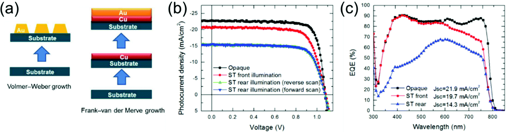
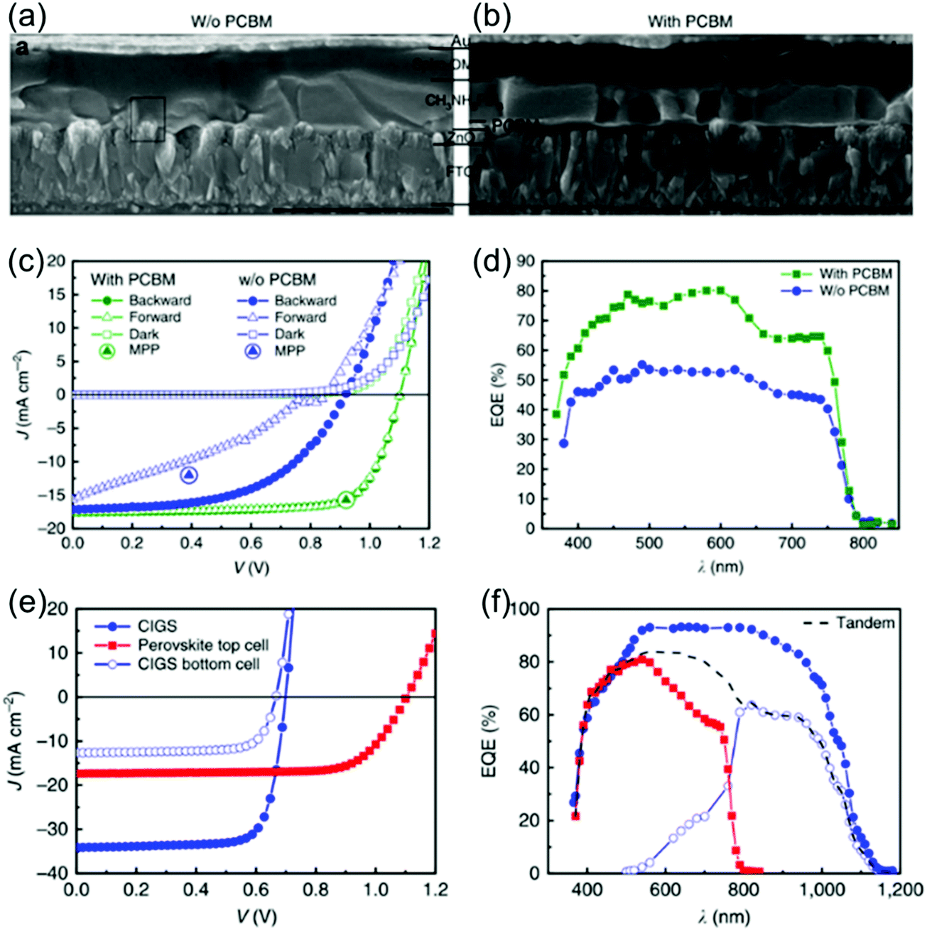
An ultra-thin metal film is an alternative approach for transparent electrodes by its good transmittance and conductivity. In 2014, Snaith and coworkers reported that the thermal-evaporation of 10 nm Au on spiro-OMeTAD and the creation of a microporous perovskite layer by partial dewetting of solution-cast films enabled ST-PSCs with ∼8% efficiency and ∼30% transmittance in the visible region.13 However, Au fails to form a uniform, continuous, and ultra-thin film due to the Volmer–Weber growth mechanism, which reduces the transmittance and increases the corresponding electrodes' sheet resistance. To improve Au's film-forming properties at a small thickness, Cheng and coworkers designed a sandwiched MoOx–Au–MoOx stack as a transparent electrode.14 MoOx has good hole injection capability and provides a good nucleation surface to form a thin yet uniform Au film. The top MoOx layer works as an anti-reflection layer. In their work, the semi-transparent MAPbI3 device shows a PCE of 5.3% with 31% average visible transmittance (AVT), and a PCE of 13.6% with 7% AVT. Parallelly, Yang and coworkers designed a MoOx (10 nm)–Au (1 nm)–Ag (10 nm)–MoOx (40 nm) multi-layer transparent top electrode for PSCs.15 The gold seeded silver film exhibited superior conductivity and optical transparency to pristine Ag or Au, owning to Au's higher surface energy. The ST-PSC illuminated from the DMD top electrode afforded 11.5% efficiency and exhibited almost no open-circuit voltage (VOC) and fill factor (FF) loss compared with the opaque device. Likewise, the Huang group designed a Cu (1 nm)/Au (7 nm) metal electrode for semi-transparent MAPbI3 PSCs.16 At a thin film, Au atoms are more strongly coupled to each other, leading to the formation of Au islands via Volmer–Weber growth during thermal evaporation. As Cu exhibits a larger surface energy of 1790 mJ m−2 than Au (1506 mJ m−2), Au atoms preferentially attach to Cu, resulting in continuous ultrathin Au films via Frank–van der Merve growth (Fig. 3a). ST-PSCs under front illumination exhibit a PCE of 16.5%, a high FF of 74.1%, and a JSC of 20.6 mA cm−2, illustrating that the Cu/Au transparent electrodes induce little loss during the collection and lateral transport of photogenerated charges (Fig. 3b). Under rear illumination, the device exhibits a PCE of 12.1% with a smaller JSC of 15.2 mA cm−2, ascribed to the less transparency of the Cu/Au/BCP layer than ITO in the visible spectrum. As Fig. 3c shows, opaque PSCs and semi-transparent devices under front illumination have comparable EQE values at short wavelengths (300–550 nm), while semi-transparent devices exhibit lower EQE at longer wavelengths (600–800 nm). When illuminated through the semi-transparent PSC, a SHJ solar cell operates with a 6.5% efficiency, leading to a sum PCE of 23.0% for the 4-T tandem device.
 | ||
| Fig. 3 (a) Scheme of Volmer–Weber growth and Frank–van der Merve growth. (b) J–V curves of opaque and semitransparent PSCs. (c) EQE curves of opaque and ST-PSCs under front and rear illumination.16 | ||
Metal nanowire offers the advantage of easy deposition in a room-temperature solvent-free process, in addition to low sheet resistance and high optical transmission. McGehee and coworkers afforded a 12.7%-efficiency semi-transparent MAPbI3 PSC with a AgNW electrode, which was first sprayed on flexible polyethylene terephthalate (PET), and then mechanically transferred to the spiro-OMeTAD layer. A sum PCE of 17.0% was realized when the semi-transparent PSC was mechanically placed on multi-crystalline Si cells (unfiltered: 11.4%, filtered: 4.3%).17 Yang, Liu, and coworkers designed a sandwiched MoO3/gold nanowire (AuNW) mesh/MoO3 transparent electrode.18 The large surface tension of MoO3 effectively improved Au's wettability, resulting in Frank–van der Merwe growth to produce an ultrathin AuNW mesh layer. The top MoO3 layer reduces the reflections at the gold layer to increase light transmission. A sum efficiency of 27.0% is realized when they mechanically stacked the 18.3% efficiency semi-transparent MAPbI3 PSC on a SHJ rear cell (unfiltered: 23.3%, filtered: 8.7%).
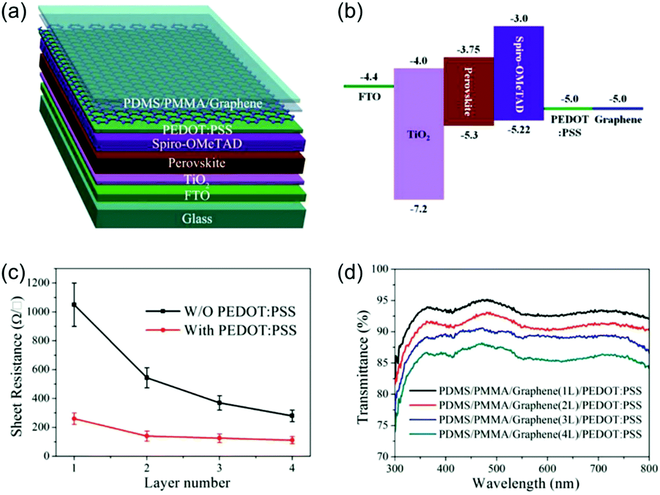
Graphene-based electrodes have a high optical transmission of 97.4% with a sheet resistance of 100 Ωsq−1.19 The Yan group pioneered laminating chemical vapor deposition (CVD) stacked graphene as a transparent electrode.20 They further coated a PEDOT: PSS layer atop graphene, which significantly improved the electrode's conductivity and provided adhesivity for lamination (Fig. 4a and b). The sheet resistance was decreased to about 260 Ωsq−1 by the doping effect of PEDOT:PSS (Fig. 4c). As Fig. 4d shows, the two-layer graphene doped with PEDOT:PSS has an Rs of 140 Ωsq−1 and a transmittance >90% in the visible region. When the layers of graphene further increase, the sheet resistance was further decreased, and the transmittance was below 90%. The ST devices with double-layer graphene electrodes show PCEs of 12.37% and 12.03% from the FTO and graphene sides, respectively (Fig. 4d).
 | ||
| Fig. 4 (a) Device architecture of a semi-transparent PSC. (b) Energy level distribution of layers of semi-transparent PSCs. (c) The sheet resistance of 1–4 layers of stacked graphene films with and without PEDOT:PSS. (d) UV-vis transmittance spectra of PEDOT:PSS doped transparent graphene electrodes.20 | ||
Lang and coworkers19 showed the successful implementation of a transparent large-area, high-quality, single-layer graphene contact upon spiro-OMeTAD in PSCs. The van der Waals forces ensured the adhesion and intimate contact of graphene on spiro-OMeTAD and enabled a 6.2%-efficiency semi-transparent cell in the absence of an additional auxiliary layer. The ST-PSC and the SHJ solar cell (unfiltered: 18.5%, filtered: 7.0%) are assembled into a 4-T tandem device, giving a higher PCE of 13.2% than the single-junction PSCs with typical Au contacts (10.2%).
In the perovskite–silicon 4-T TSCs, the top PSCs are commonly stacked onto the bottom c-Si devices with an air gap. Due to the significant refractive indices mismatch between the air and functional layers, a part of the NIR light would be reflected to the PSCs. In 2018, Jaysankar and coworkers proposed a refractive index matching layer (IML) to replace the unfavourable air gap.21 The introduction of the optical spacer increased the transmission of NIR light through the top PSC and boosted the photocurrent of the c-Si bottom solar cell.
Although mainstream 4T TSCs adopt the “planar structure” aforementioned, in principle they can be constructed using other configurations. For example, an optical splitter is a multi-layer beam splitter with high reflection in the short-wavelength range and high transmission in the long-wavelength range. By splitting the incident solar spectra and distributing them to each subcell, solar energy can be utilized more effectively. Via an optical splitter, subcells in 4-T structure can be set spatially separated yet optically coupled (Fig. 5). The optical splitter is fabricated by sputtering multi-layer dielectric oxides with high (n ∼ 1.9–2.2) and low (n ∼ 1.5) refractive indices on both sides of the glass. The cut-off wavelength can be controlled by altering the number and thickness of the stacking layers. The Yamamoto group designed a series of optical splitters with cut-off wavelengths of 550, 600, and 640 nm, respectively. They achieved 28%-efficiency 4-T devices based on 7.5%-efficiency MAPbI3 PSCs and SHJ solar cell (unfiltered: 25.2%, filtered: 20.5%) with an optical splitter featuring 550 nm cut-off wavelength.22
 | ||
| Fig. 5 (a) Scheme of the optical splitting system, (b) measurement setup of an optical splitting system, and (c) J–V curves of SHJ and perovskite solar cells with and without a splitter.22 | ||
2.2 Perovskite–silicon 2-terminal TSCs
The 2-T configuration, where subcells are constructed as a single integrated unit, allows simple electrical integration and bypasses additional transparent electrodes. Nonetheless, the monolithic approach requires a tunnelling/recombination interlayer that can effectively facilitate the flow of photogenerated carriers between two subcells. A reasonable tunnelling/recombination layer should introduce small electrical and optical losses and low processing costs.Si is an indirect-Eg semiconductor. It is common to design tunnelling junctions consisting of two heavily doped p++ and n++ regions for charge recombination. McGehee and coworkers demonstrated the first 2-T monolithic perovskite–silicon TSC with an inter-band tunnelling junction.23 To form n++/p++ tunnelling junction, they deposited heavily doped n++ hydrogenated amorphous silicon (a-Si:H) on the p++ emitter via plasma-enhanced chemical vapor deposition (PECVD) and subsequently thermally annealed the a-Si:H layer to activate the dopants. Besides, a 2–3 nm-thick intrinsic a-Si layer was inserted between the p++ emitter and n++ amorphous Si layer to mitigate the dopant interdiffusion and prevent the degrading of the tunnelling-junction conductivity. They obtained a PCE of 13.7% and a VOC of 1.58 V for the 1 cm2, 2-T MAPbI3/Si tandem device. The slow current-dynamics and corresponding hysteresis of the tandem device resembled the sluggish dynamics of the MAPbI3 PSC, which indicated that the perovskite subcell limited the JSC of the TSCs. The n++/p++ tunnelling junction demonstrated high shunt resistances and potentially facilitated the fabrication of large-area tandems. However, this Si-based tunnelling junction requires an additional PECVD step and introduces parasitic optical absorption.
The transparent conductive oxide (TCO) recombination layer is an alternative for constructing 2-T devices, like indium-doped tin oxide (ITO) and indium-doped zinc oxide (IZO). Before 2015, the reported c-Si/perovskite tandems usually required high-temperature (∼500 °C) processing to sinter mesoporous TiO2. This processing is not compatible with the best-performing SHJ technology, as a-Si:H requires the temperature to remain below 200 °C. To tackle this problem, Grätzel and coworkers sputtered the ITO recombination layer and used the atomic layer deposition (ALD) SnO2 layer as the electron selective contact for PSCs to construct a 2-T perovskite-SHJ tandem architecture.24 The 2-T devices demonstrate an efficiency of 19.9%, with a JSC of 14 mA cm−2, a VOC of 1.78 V, and FF of 79.5%. In their work, the SHJ structure's potential is not completely fulfilled due to the absence of a pyramid texture on the Si wafer, as the solution processing of PSCs requires a smooth substrate underneath. The Ballif group chose an IZO recombination layer in the 2-T monolithic perovskite–Si tandem cell, which is inspired by the successful application of the IZO recombination layer in organic tandem solar cells.25 They presented low-temperature-processing MAPbI3/SHJ monolithic TSCs with efficiencies of 19.2% with an aperture area of 1.22 cm2 and 21.2% with 0.17 cm2 aperture area, respectively. According to transfer matrix simulations, the PSCs can achieve a maximum current density of the top cell with a ∼40 nm thick IZO recombination layer and a 150 nm thick spiro-OMeTAD layer, and the SHJ bottom cell needs to be textured to harvest more infrared photons. Impediments to more advances in TCO interlayer include substantial parasitic absorption due to free-carrier absorption at long wavelengths and the proneness of carriers to be funnelled to shunt paths along the recombination layer, which limits large-area fabrication.
In general, an interface (tunnelling or recombination) layer makes electrical contact between the top and the bottom subcells but incurs higher fabrication costs and parasitic absorption. The “interlayer-free” concept offers the advantages of more straightforward processing and reduced optical losses. For the first time, Baillie group demonstrated a monolithic planar-MAPbI3 perovskite-homo-junction silicon tandem without the use of an additional interface layer.26 The mechanism is that the solution-processed SnO2 layer serves as an electron transport layer for the perovskite top cell and as a recombination layer between the perovskite top cell and the Si bottom cell. The champion 2-T device with a 4 cm2 area achieves a steady-state efficiency of 20.5% when the PDMS foil is applied. Besides, upscaling to large-area devices becomes straightforward as the monolithic tandem device relies on the p++ emitter instead of SnO2 for lateral conduction. Thereby, a steady-state PCE of 17.1% can be achieved in a large area of 16 cm2. They further optimize the device structure in some aspects. First, a new metal grid design is used for demonstrating 16 cm2 large-area devices. Second, the planar homojunction silicon subcell is replaced with a textured homojunction silicon bottom cell. Third, a mixed perovskite absorber (FAPbI3)0.83(MAPbBr3)0.17 is used instead of MAPbI3, which can improve the VOC of the tandem device and reduce hysteresis, owing to the larger Eg and better quality of mixed perovskite. Correspondingly, they demonstrated a 16 cm2-area perovskite–homojunction silicon tandem device with a high PCE of 21.9% under reverse scan and a high FF of 78%.27
Parasitic UV absorption and UV-induced degradation by spiro-OMeTAD in PSCs hinder device performance and stability when the perovskite cell is a top cell of perovskite–Si TSCs. Hence, the Baillie group applied textured polydimethylsiloxane (PDMS) films that incorporate a down-shifting material, (Ba, Sr)2SiO4:Eu2+ micron phosphor, in front of the monolithic 2-T perovskite–homojunction silicon tandem device (Fig. 6a).28 (Ba,Sr)2SiO4:Eu2+ phosphor had high luminescent efficiency with broad UV absorption and short decay time, which is suitable for a down-shifting material in photovoltaics. This film served multiple purposes: antireflective control for the top cell, light trapping in the Si cell, and absorbing UV and reemitting green light with high quantum yield. Fig. 6b shows the PL spectra (green curve, λex = 370 nm) and photoluminescence excitation spectra (black curve, λem = 517 nm) of (Ba,Sr)2SiO4:Eu2+. The green emission ranges from 460 to 580 nm, and is peaked at 517 nm, corresponding to a Commission Internationale de I’Eclairage (CIE) chromaticity coordinate of (0.1891, 0.6441). The emission of Eu2+ ions is due to the transition from the relaxed 4f65d1 state to 4f7 ground state. The PL decay curve of (Ba,Sr)2SiO4:Eu2+ phosphor (λex = 405 nm), is detected at 520 nm at room temperature (Fig. 6c). When applied onto a 4 cm2 monolithic perovskite–silicon TSC, PCE was improved from 20.1% (control device without PDMS layer) to 22.3% (control device with pure PDMS layer) to 23.1% (experimental device with 0.5 wt% (Ba,Sr)2SiO4:Eu2+ doped PDMS). Moreover, the champion device maintained 90% of the initial performance after 648 h UV exposure at 5 mW cm−2. Catchpole and coworkers also demonstrated a monolithic 2-T perovskite–Si tandem by straightforward integration of PSCs and Si solar cells without an additional layer (Fig. 7a). This interlayer-free device is enabled by highly conductive contact between ALD n-type TiO2 and P-Si.29 A possible reason is the substantial density of localized midgap states at the interface between p-Si and TiO2. These interfacial states can facilitate band to band tunnelling at reverse bias and work as generation–recombination centers at all bias voltages. Electrons move into/out of the defect states via local capture/emission and tunnelling in this circumstance. Fig. 7b shows the photovoltaic J–V performance exhibited by the highest-performing poly-Si tandem cell and the corresponding photovoltaic metrics. The corresponding monolithic 2-T perovskite (Cs0.05Rb0.05FA0.765MA0.135PbI2.55Br0.45)/SHJ tandems demonstrate an efficiency of 24.1% at reverse scan, with a VOC of 1.763 V, a JSC of 17.8 mA cm−2, and a FF of 78.1%.
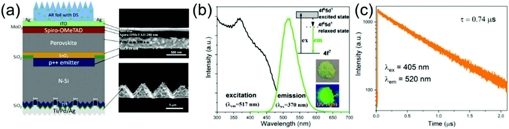 | ||
| Fig. 6 (a) Schematic illustration of perovskite–silicon homojunction solar cells with a down-shifting AR PDMS layer. Cross-sectional SEM image of the perovskite top cell and the rear textured silicon bottom cell. (b) Excitation and emission spectra of the (Ba,Sr)2SiO4:Eu2+ phosphor (inset: schematic diagram of the Eu2+ 4f–5d transition and photos of phosphor powder under ambient light and UV light (365 nm). (c) Decay curve of the Eu2+ emission in the (Ba,Sr)2SiO4:Eu2+ phosphor.28 | ||
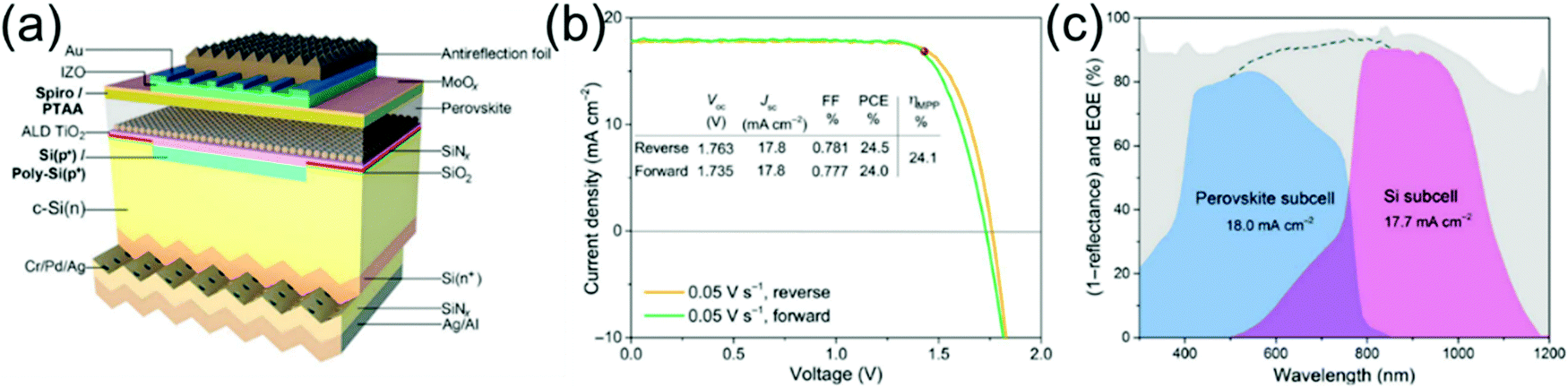 | ||
| Fig. 7 (a) Scheme of the interlayer-free monolithic perovskite–c-Si tandem solar cell. (b) J–V curve of the tandem device with both reverse and forward scanning at 0.05 V s−1 based on heterojunction poly-Si subcell. (c) Absorbance (1-reflectance) of the tandem device (gray), EQE of the perovskite top cell (blue), and the c-Si bottom subcell (pink).29 | ||
It is possible to position an electrically inert but optically textured layer with an appropriate refractive index directly atop the top contact of TSC to improve light absorption. Albrecht and coworkers employed textured LM foils on the front side of a TSC. The LM foil significantly improved the PCE of the 2-T perovskite-SHJ tandems from 23.4% to 25.5%.30 Besides, through simulations, they predicted a slightly narrower optimal Eg of the perovskite top sub-cell is needed to match a textured Si device compared with a flat device, and the strong interdependency between Eg and the texture position in the monolithic 2-T device. Their simulations showed that a 32.5% efficiency is realistically achievable with a 1000 nm 1.66 eV-Eg perovskite atop a both-side silicon device. Snaith and coworkers incorporated an optical interlayer consisting of nanocrystalline silicon oxide (nc-SiO2:H) to mitigate the optical drawback of a flat silicon substrate and increase bottom-cell current density.31 The 110-nm nc-SiO2:H interlayer with a refractive index of 2.6 resulted in 1.4 mA cm−2 current density gain in the silicon bottom cell. The anisotropic nature of the nc-SiO2:H interlayer with high transversal and low lateral conductivity supports the further reduction of top-cell shunting via shunting quenching. The champion 1 cm2 monolithic 2-T perovskite–silicon tandem cell exhibits a total current density of 38.7 mA cm−2 under AM 1.5G irradiation, and a certified stabilized PCE of 25.2%.
Surface texture can also be realized by using c-Si wafers with μm-sized pyramids. Such a texture improves light in-coupling by minimizing reflections off the front surface while scattering the light within the solar cell to enhance light trapping. However, most monolithic 2-T perovskite–silicon tandems use Si wafers featuring a smooth front side and textured backside to meet the requirement of PSC wet processing. Difficulties of depositing perovskite via solution techniques atop μm-sized Si pyramids include uncovered Si pyramids, large shunt paths, and inefficient charge collection. Besides, conventional surface-passivation techniques are incompatible with the rough perovskite surfaces. This configuration, nonetheless, limits light-trapping functions and requires additional anti-reflection foils, the effectiveness of which may be compromised by encapsulation. Moreover, perovskite–silicon tandems with a polished wafer surface have a cost issue, as industrial Si wafers are typically etched and textured on both sides, and chemical-mechanical polishing is cost-prohibitive.
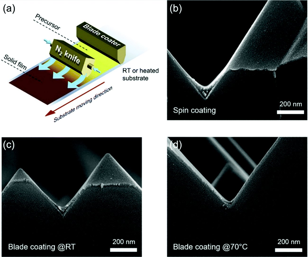
Sargent and coworkers constructed high-performance 2-T perovskite tandems based on fully textured SHJ bottom cells (Fig. 8a).32 They increased the depletion width by three times at the bases of silicon pyramids to facilitate charge collection in μm-thick perovskites. The JSC of the PSC increases with the thickness of the perovskite layer. The experimental JSC value (certified ∼19.3 mA cm−2) of the ∼1.1 μm-thick perovskite is thereby only within 10% deviation of the theoretical limit (Fig. 8b). As Fig. 8c shows, spectrally weighted reflectance is calculated from the AM 1.5G spectrum at 350–900 nm. They observed that the benefit to reflection began to saturate when the pyramid size was reduced to 2 μm, suggesting the solution-processing techniques of perovskite can be integrated with textured silicon. They also increase carrier diffusion length and suppressed phase segregation by anchoring 1-butanethiol as a self-limiting passivator (SLP) on the perovskite surfaces. The SLP method increases FF from 72% to 77% (Fig. 8d). EQE characterization demonstrates the advantage of switching from a polished front side to a double-side textured architecture (Fig. 8g and h). The introduction of a front texture reduced reflection losses and exhibited efficient light trapping. The device demonstrated a certified PCE of 25.7% and negligible performance loss after the thermal stability test (400 hours, 85 °C) and after MPP tracking (400 hours, 40 °C) (Fig. 8e and f). Huang and coworkers use a blade-coating technique to deposit PSCs' layers on the double-side-textured silicon cells with sub-μm pyramids (Fig. 9).33 These pyramids with shrunken size are rough enough to scatter light within the silicon relative to large-size pyramids. A N2 knife helps remove solvent vapor, facilitating a quick transition of solution into solid during the blading process (Fig. 9a). When PTAA is spin-coated on a silicon bottom cell, the resulting layer is non-uniform with a thickness of 45 nm in the valleys but a thickness of 8 nm on the pyramids (Fig. 9b). Even with N2-assisted drying, blade coating PTAA at room temperature results in a non-uniform layer (Fig. 9c). When the substrate temperature was elevated to 70 °C, the solvent's accelerated evaporation makes PTAA more uniform on the textured silicon surface (Fig. 9d). The high-throughput blade-coating process can deposit both a conformal hole transport layer and a planarizing perovskite layer that thoroughly covers the textured silicon with increased substrate temperature. This work elongates the path length of long-wavelength light in the silicon and reduced reflection loss to afford 2-T tandems with a JSC >19 mA cm−2 and an efficiency of 26.2%.
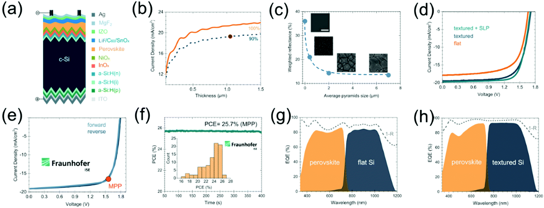 | ||
| Fig. 8 (a) Structures of solution-processed perovskite–textured silicon tandem. (b) Calculated JSC values of the perovskite cells as a function of perovskite layer thickness. The red dot represents the EQE-integrated JSC value in the textured tandem top cell. (c) Weighted reflectance as a function of c-Si pyramid sizes. The SEM images of different texturing sizes are shown in the insets (scale bar, 2 mm). (d) J–V characteristics of flat, textured, and SLP-treated textured tandems. (e) J–V curves of certified SLP-treated textured tandems. (f) MPP tracking of certified SLP-treated textured tandems and PCE distributions of 88 individual tandem devices. (g) EQE of the flat devices. (h) EQE of the textured devices.32 | ||
 | ||
| Fig. 9 (a) Scheme of N2-assisted blade coating. (b–d) SEM images of PTAA on textured silicon bottom cells deposited by (b) spin coating, (c) N2-assisted blade coating with the substrate at room temperature, and (d) N2-assisted blade coating with the substrate at 70 °C. The three visible layers are the silicon wafer, ITO front electrode of the silicon cell, and PTAA hole-transport layer.33 | ||
Note that the bifacial c-Si solar cell and module technology have received considerable attention, which collects light from both the front and rear sides. The bifacial power gain can be up to 50%,34 and is highly dependent on the albedo of the surroundings and installation geometry.35 The concept of bifacial cell and module can be naturally transferred to perovskite–c-Si tandems for both 2-T and 4-T configurations.36–38 In 2021, Sargent, Wolf, and co-workers systematically studied the performance of bifacial 2-T perovskite–c-Si tandems. Because of the additional incident light from the rear side, the optimized Eg of perovskite is reduced to 1.59–1.62 eV. Thus, the bromide content is reduced compared with that in the wide band gap perovskite, which would relax the stability issue coming from the halide segregation.39
Cation substitution with Cs or DMA can widen the Eg of perovskite and prevent the large fraction of Br. For instance, the Zhou group reported high-efficiency monolithic 2-T perovskite–Si tandems by tuning the Eg and the optical density of perovskite absorbers.42 Four different perovskite absorbers (FA0.48MA0.37Cs0.15PbI2.23Br0.77, FA0.57MA0.43PbI2.04Br0.96, FA0.5MA0.38Cs0.12PbI2.04Br0.96, and FA0.51MA0.38Cs0.11PbI1.85Br1.15) were adopted to adjust the Eg of perovskite absorbers from 1.65 to 1.72 eV. The FA0.5MA0.38Cs0.12PbI2.04Br0.96 film presented a much lower trap density of 1.13 × 1016 cm−3 than FA0.57MA0.43PbI2.04Br0.96 (5.7 × 1016 cm−3), presumably because the small amount of Cs acts as nucleation sites, effectively promotes crystal growth and suppresses defect formation. To maximize the potential of (FA, MA, Cs) PbX3, they optimized the residual PbI2 content in the film, the thickness of the perovskite layer, and the SnO2 electron transport layer. ST-PSCs with a 410 nm FA0.5MA0.38Cs0.12PbI2.04Br0.96 layer and a transparent MoOx/ITO transparent electrode exhibited an efficiency of 13.09%. The 2-T TSCs based on FA0.5MA0.38Cs0.12PbI2.04Br0.96 and SHJ delivered a PCE of 22.22% and retained over 85% of their original efficiency after the long-term stability test (500 h).
MAPbCl3 has a wider Eg of 2.88 eV and higher stability than its Br and I counterpart. However, incorporating Cl into perovskite precursor solutions typically cannot increase Eg but increases the perovskite domain size, because the formation and outgassing of MACl alter the crystal nucleation and growth dynamics. Hence, the Cl concentrations in the perovskite film were below the detection limit of energy-dispersive X-ray spectroscopy (EDX) and X-ray photoelectron spectroscopy (XPS), even when a large portion of Cl was incorporated in the precursor solution. McGehee and coworkers alloyed 2–5 mol% MAPbCl3 into the lattice of FA0.75Cs0.25Pb(I0.85Br0.15)3,43 and thereby increased the solid solubility of Cl and the PVSK Eg from 1.63 to >1.67 eV (Fig. 10a). In their work, the Cl to Pb ratio in solid films is increased with the increasing fraction of Cl in the precursor solution, with the grain domain size barely enlarged. Specifically, Cs0.25FA0.75Pb(I0.85Br0.15)3:5% MAPbCl3 has a lattice constant of ∼6.24 Å, like that of Cs0.25FA0.75Pb(I0.8Br0.2)3 and smaller than that of Cs0.25FA0.75Pb(I0.85Br0.15)3 (Fig. 10b and f). This is because the lattice constant of the host perovskite was reduced by Cs and Br, making Cl closer to the ideal size for the X-site in the lattice. Consequently, Cl is located in the perovskite lattice and increased Eg, instead of being sacrificed in an MACl volatile phase. The Cl element in the triple-halide films was uniformly distributed through the entire film thickness (Fig. 10c). The bandgap decreases at high Cl content due to double-phase segregation into high Br/Cl phase and high I/Br phase (Fig. 10d–f). The extension from double-halide (I, Br) to triple-halide (I, Cl, Br) significantly increases photocarrier lifetime and charge-carrier mobility and effectively suppresses light-induced phase segregation. This strategy reduced the VOC loss of opaque 1.67 eV-Eg PSCs by 100 mV and boosted the PCE from ∼18% to 20.3%. A PCE of 27.0% and a VOC of 1.886 V were thereby achieved in 1 cm2 monolithic 2-T tandems by pairing the perovskite top cells with SHJ bottom cells.
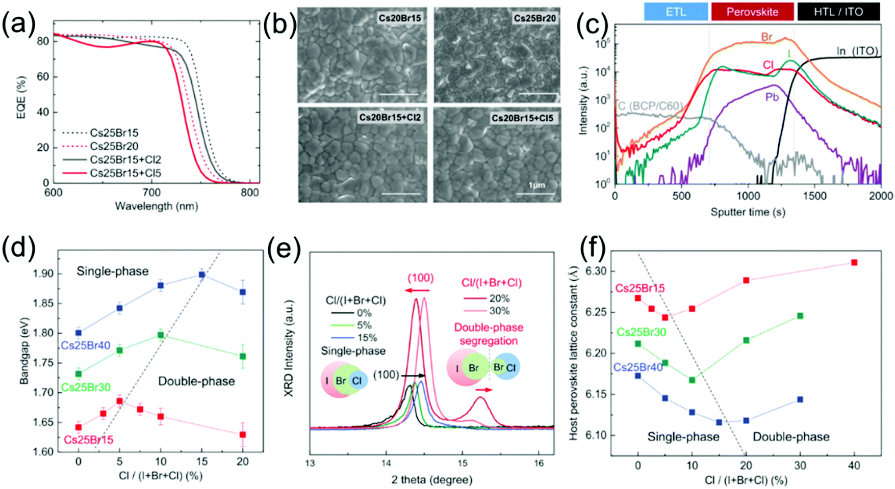 | ||
| Fig. 10 (a) EQE curves of perovskite with and without Cl. Cs25Br15 and Cs25Br20 refer to Cs0.25FA0.75Pb(I0.85Br0.15)3 and Cs0.25FA0.75Pb(I0.8Br0.2)3, respectively. Cs25Br15 + Cl2 and Cs25Br15 + Cl5 refer to the triple-halide perovskites with 2 or 5 mol% MAPbCl3 in the Cs25Br15, respectively. (b) Top-view SEM images of double-halide and triple-halide perovskites. (c) The uniform distribution of halides throughout the entire film thickness of the triple-halide perovskite (Cs25Br15 + Cl5). (d) Evolution curves of the band gap for triple-halide perovskite films with an increased ratio of Cl/(I + Br + Cl), based on Cs25Br15 (red), Cs25Br30 (green), and Cs25Br40 (blue), respectively. The dashed line delineates the single-phase and double-phase zones corresponding to bandgap raising and reducing, respectively. (e) Shifting and splitting of the XRD (100) peaks shows the transition from single-phase triple-halide alloy to double-phase segregation in Cs25Br40 with increased Cl content. (f) Curves of host perovskite lattice constant with increasing ratios of Cl/(I + Br + Cl). The dashed line delineates the single-phase and double-phase zones corresponding to band gap increasing and reducing, respectively.43 | ||
The two-dimensional (2D) phase was used to stabilize wide-Eg perovskite, where sheets of [PbX6]2− octahedra are separated by long-chain or aromatic molecules that act as a passivation agent. For example, n-butylammonium iodide (n-BAI) and phenethylammonium iodide (PEAI) are common 2D additives. Snaith and coworkers introduced n-butylammonium (BA) cations into (FA0.83Cs0.17Pb(IyBr1−y)3) perovskite. The 2D perovskite platelets were formed and interspersed among highly orientated 3D perovskite grains, suppressing non-radiative charge recombination. The device with an optimal concentration of BA cations exhibited an average stabilized PCE of 17.5 ± 1.3% with a 1.61 eV-Eg perovskite and 15.8 ± 0.8% with a 1.72 eV-Eg perovskite. Unencapsulated devices retained 80% of their post burn-in efficiency after 1000 h in air, while the encapsulated device retained 80% after nearly 4000 h.44 Shin and coworkers incorporated binary additives, Pb(SCN)2 and PEA(I0.25SCN0.75), into 1.68 eV-Eg (FA0.65MA0.2Cs0.15)Pb(I0.8Br0.2)3 perovskite and thereby delivered a 26.7%-efficiency, stable monolithic 2-T perovskite–Si TSCs.45 The 2-T devices retained >80% of their initial PCE (20.7%) after 1000 hours of continuous illumination (underneath a sulfur plasma lamp at ∼0.8 sun). Anion engineering of phenethylammonium-based 2D additives was critical for controlling the structural and electrical properties of the 2D passivation layers bearing a PbI2 framework. Pb(SCN)2 accelerates the growth of 3D perovskite grains. The 2D additive PEA(I0.25SCN0.75) enables the formation of 2D-phase perovskite both on the surface and at grain boundaries, compared with the sample with Pb(SCN)2 forming only surface 2D phases.
Al-Ashouri and coworkers recently demonstrated a monolithic perovskite–silicon tandem with a certified record-high PCE of 29.15%,46 surpassing the best silicon single-junction cell (26.7%). The 1.68 eV-Eg perovskite absorber remained phase-stable under illumination through the synergy of fast hole extraction and minimized nonradiative recombination at the hole-selective interface. These features were afforded by a self-assembled, methyl-substituted carbazole monolayer (Me-4PACz) as the hole-selective layer in the PSC. The accelerated hole extraction went along with a low ideal factor of 1.26, a high single-junction FF of 84%, and a high tandem VOC of 1.92 V. In air, the tandem device without encapsulation retained 95% of its initial efficiency after 300 hour of operation.
Because of the series connection feature and the spectral mismatch of solar simulators, it is difficult to measure the photovoltaic properties of 2-T tandem devices. Kim and coworkers designed three-terminal (3-T), monolithic perovskite–Si tandem cells, where the ITO recombination layer was also used as an additional electrode for characterization47 (Fig. 11a and b). The top subcell was a semi-transparent perovskite solar cell with MAPbI3 as the high-energy absorber, deposited on a flat silicon bottom cell with a textured backside. With the 3-T architecture, the J–V characteristics of each subcell and the tandem cell can be measured independently; the EQE of each subcell can be accurately measured without any light/potential bias or filtration of the probing light. Through optical engineering and bandgap tuning, the best monolithic 3-T perovskite (MAPb(I0.95Br0.05)3)/SHJ tandem cell exhibits a high PCE of 23.5% and retains 97% of the initial efficiency stored in the dark after 100 days.
 | ||
| Fig. 11 (a) Cross-sectional FESEM images of perovskite top cell and silicon bottom cell, and (b) schematic illustrations of the monolithic perovskite–Si tandem cell and circuits of the 2,3-T architecture.47 | ||
The monolithic 2-T perovskite–perovskite–silicon triple-junction solar cells can be a low-cost alternative of III-V semiconductor based triple-junction solar cells, as the latter device requires complicated and costly manufacturing processes. Snaith and coworkers predicted that triple-junctions based on 1.95 and 1.44 eV perovskite subcells and a 1.1 eV silicon bottom cell have an efficiency potential of 38.8%.48 The Ballif group realized a proof-of-concept 2-T perovskite–perovskite–silicon triple-junction device by monolithically growing two perovskite cells on double-side textured silicon wafers.49 They employed an evaporation-spin coating sequential process to deposit the perovskite absorbers, enabling the conformal growth of all the layer stacks directly on the μm-sized pyramids of the Si bottom cell. The triple-junction devices exhibited a VOC of ∼2.7 V, an equivalent cumulative current density of 38.8 mA cm−2, and MPP tracked efficiency of 13.2%.
3. Perovskite–perovskite TSCs
Perovskite–perovskite tandems offer a route to high efficiency and reserve the strengths of low-cost, low-temperature, and low environmental impact fabrication and the possibility of lightweight and flexible form of both subcells. Perovskite has compositional versatility and thus highly adjustable Eg, which offers the potential of realizing high-performance perovskite-perovskite tandems. For instance, the Eg of the Pb-based perovskite can be increased from 1.58 (pure I) to 2.2 eV (pure Br) by substituting I with Br in MAPbI3. The Zhou group pioneered in constructing bottom-up solution-processed 2-T all-perovskite TSCs, where two MAPbI3 subcells are bridged by a spiro-OMeTAD/PEDOT: PSS/PEI/PCBM: PEI charge recombination layer. Despite the low PCE of 7%, this device yields a high VOC of 1.89 V close to the sum of the two MAPbI3 subcells.50 The Im group fabricated 2-T MAPbBr3-MAPbI3 TSCs by laminating single-junction MAPbBr3 and MAPbI3 planar solar cells.51 In their work, P3HT and poly[bis(4-phenyl)(2,4,6-trimethylphenyl)amine] (PTAA) hole conductors with Li-TFSI and t-BP additives improved conductivity and reduced charge-transport barriers due to the assistance of the Li/Li+ redox shuttle. Despite the high VOC of 2.25 V, the monolithic 2-T MAPbBr3–MAPbI3 TSCs gave a low JSC of 8.3 mA cm−2 and a frustrating sum PCE of 10.8%, suggesting that the combination of only wide-Eg Pb perovskite absorbers fundamentally limits device performance.The mixed Sn–Pb perovskite presents the bandgap bowing effect, which means the mixed perovskite can present a lower bandgap than those of its Sn-free and Pb-free counterparts. Alloying Pb and Sn in metal halide perovskites can narrow the Egs down to 1.17 eV for MASn1−xPbxI3 (x = 0.25 and 0.5). In principle, the low-Eg Sn–Pb perovskite could be an ideal candidate as the bottom subcell, opening a pathway for high-performance perovskite–perovskite tandems. Recent optical and device modelling shows that all-perovskite tandems based on 1.22 and 1.80 eV PSCs have a potential to reach 33.4% efficiency with EQE over 90% and VOC of 2.17 eV, rendering this technology potentially competitive with perovskite–Si tandems.48 To achieve high-performance all-perovskite tandems, low-Eg Sn–Pb perovskite should have a large thickness to harvest sufficient photons, and long carrier diffusion lengths to ensure efficient charge transport and extraction. However, narrow Eg Sn or Sn–Pb PSCs lag far behind wide Eg PSCs currently, which is the major obstacle hindering the advances of all-perovskite tandems. Recently, scientists have carried out composition engineering, additive engineering, solvent engineering, and interface engineering to improve Sn–Pb perovskite based single-junction and tandem devices.
In the early times, devices based on Sn-containing perovskites performed much worse than their pure-Pb counterparts, even though Sn-containing perovskite absorbs a larger fraction of the solar spectrum. Early in 2012, the Shum group invented the first Sn (CsSnI3) PSCs, which delivered a PCE of 0.9%.52 In 2014, the Kanatzidis group reported that PSCs based on 1.30 eV-Eg CH3NH3SnI3 and 1.17 eV-Eg MASn0.75Pb0.25I3 afforded efficiencies of 5.44% and 7.37%, respectively.53 The disappointing performance of Sn or Sn–Pb based PSCs is associated with both material and device issues. First, Sn and Sn–Pb perovskites have smaller absorption cross-sections than Pb perovskites, which requires a thick-film Sn or Sn–Pb perovskite absorber to achieve high EQE and in turn long carrier diffusion lengths for efficient charge extraction. Second, the Sn-substituted perovskite typically crystallizes more quickly than Pb-based perovskite, resulting in inferior-quality films. Last but not least, the facile oxidation of Sn2+ to Sn4+ reduces the device performance and stability.
To improve the film quality of Sn-based perovskite, Huang and coworkers reported a simple Pb-assisted two-step spin-coating method. In the control group without PbI2, a sequential deposition of pure SnI2 and MAI afforded MASnI3 film with cracks and discontinuous grains.54 By contrast, the perovskite film is uniform and crack-free with the addition of PbI2. Therefore, the MASn0.5Pb0.5I3 PSCs achieved a PCE of 13.6% with high reproducibility. Jen and coworkers further improved the performance of low-Eg Sn–Pb PSCs via integrated composition, process, and interface engineering.55 The solvent-washing methodology with a DMSO-based co-solvent system effectively retards the growth of Sn–Pb perovskites and helps form homogeneous and smooth films by forming the SnI2·DMSO intermediate phase. MAPb0.75Sn0.25I3 with ∼1.35 eV Eg was chosen after the investigation of surface morphology and optoelectronic properties of MAPb1−xSnxI3 perovskites with different x values. As the partial substitution of MA with FA stabilizes the Sn–Pb perovskite, the final composition they chose is 1.33 eV Eg FA0.5MA0.5Pb0.75Sn0.25I3. The corresponding devices achieved a PCE of 14.19% and retained >94% of its initial PCE after 30 days in an inert atmosphere. The coupling of the Sn–Pb perovskite bottom subcell (unfiltered: 14.19%, filtered: 5.56%) and a semi-transparent MAPbI3 (13.52%) top subcell endowed the 4-T device with an encouraging PCE of 19.08%.
Via cation and device engineering, Snaith and coworkers demonstrated a 14.8% efficiency for Sn–Pb PSCs. They implemented a technique of precursor-phase antisolvent immersion to deposit uniform FASn0.5Pb0.5I3 film.56 The mixed solvents of DMSO and DMF with low-vapor pressure retard crystallization via the formation of precursor complexes, followed by an immediate antisolvent bath and gentle heating to crystallize the perovskite. The partial substitution of FA with Cs effectively improved the PCE from 10.9% to 14.1%. The combination of the 1.2 eV Sn–Pb perovskite (FA0.75Cs0.25Sn0.5Pb0.5I3) cell and 1.8 eV Eg perovskite cell (FA0.83Cs0.17PbI0.15Br0.15) demonstrates a 17.0%-PCE monolithic 2-T TSC. They also fabricated 20.3% efficiency small-area all-perovskite 4-T tandems based on a semitransparent 1.6-eV Eg FA0.83Cs0.17Pb(I0.83Br0.17)3 front cell (filtered: 15.8%) and the FA0.75Cs0.25Sn0.5Pb0.5I3 bottom cell (unfiltered: 14.8%, filtered: 4.5%).
The development of mixed Sn–Pb PSCs can draw lessons from the recent progress of the Pb-free PSCs.57 First, FASnI3 is more stable than MASnI3 to work as the Sn source. Second, SnF2 additives are useful for increasing carrier lifetime (by reducing Sn vacancy and background hole density), changing the energetics of the material, and improving the film morphology and stability. Third, hole transporting layers using Li or Co salts as dopants may pose damage to Sn-containing perovskite. Accordingly, Yan and coworkers employed 1.25 eV Eg (FASnI3)0.6(MAPbI3)0.4 absorber, SnF2 additives, and a PEDOT:PSS hole transporting layer to fabricate Sn–Pb inverted PSCs. Fig. 12a sketches the steps of forming the precursors for one-step deposition of mixed Sn–Pb perovskite thin fims, consisting of the FASnI3 precursor with the MAPbI3 precursor at different molar ratios. MAPbI3 and FASnI3 films both contain many large grains, yet with some small ones (Fig. 12b and c). As a comparison, the (FASnI3)0.6(MAPbI3)0.4 film contains relatively smaller but more uniformly distributed grains (Fig. 12d). The device based on (FASnI3)0.6(MAPbI3)0.4 exhibited a PCE of 15.08% with good reproducibility and negligible hysteresis.58 The Sn–Pb perovskite exhibits a carrier lifetime of 0.7 ns, much longer than FASnI3 (0.2 ns), but much shorter than MAPbI3 (109 ns). The low-Eg PSCs show relatively low spectral response in the NIR region, which is resulted from the short carrier lifetime (<20 ns) and the relatively thin (∼400 nm) Sn–Pb perovskite film. By optimizing the precursor solutions, Yan and coworkers simultaneously increased the grain size, crystallinity, and carrier lifetime to 255 ns at a thickness of 620 nm for the perovskite layer. The low-Eg PSCs achieved a PCE of 17.5%, and a JSC of 28.7 mA cm−2 with EQEs of >70% in the NIR range.59 When it was mechanically stacked with a FA0.3MA0.7PbI3 (∼1.58 eV) front cell, a maximum PCE of 21.2% at reverse scan was demonstrated for the 4-T all-perovskite tandem cell. Yan and coworkers further incorporated 2.5% Cl into (FASnI3)0.6(MAPbI3)0.4, which simultaneously enlarged the grains, increased crystallinity, and functionalized grain boundaries. Via photothermal deflection spectroscopy (PDS) characterization, they found the incorporation of 2.5% Cl reduced Eu from 27.9 meV (the undoped perovskite device) to 23.9 meV (the experimental device), illustrating that Cl reduced electronic disorder.60 Transient photocurrent measurement illustrated that Cl incorporation effectively increased the minority carrier lifetime. The inverted planar Sn–Pb PSCs with ∼750 nm active layer demonstrated a PCE of 18.40%, a VOC of 0.850 V, and a high JSC of 29.31 mA cm−2 with negligible J-V hysteresis. By combining this narrow-Eg PSC, wide-Eg FA0.8Cs0.2Pb(I0.7Br0.3)3 PSC, and ultra-flat and smooth Ag/MoOx/ITO ICLs, the monolithic 2-T tandem device achieved PCEs of 21.0% and promising operational stability. Likewise, the incorporation of Br endowed the 1.27 eV Sn–Pb perovskite with a high PCE of 19.1% and a small VOC loss of 0.384 V.61
 | ||
| Fig. 12 (a) Scheme of the formation of (FASnI3)1−x(MAPbI3)x precursor. (b–d) SEM images of (FASnI3)1−x(MAPbI3)x perovskite films (x = 0.0, 1.0, and 0.4).58 | ||
Commonly used Sn-based narrow-Eg perovskite has shorter carrier diffusion lengths and lower absorption coefficient than the Pb-based perovskite. In Sn-containing PSCs, electrons exhibited much shorter diffusion length than holes. Huang and coworkers incorporated 0.03 mol% cadmium ions (Cd2+) into FA0.5MA0.45Cs0.05Pb0.5Sn0.5I3 perovskite to de-dope Sn–Pb perovskite and reduce the electron trap density, which effectively enhances the recombination lifetime, electron mobility, and electron diffusion length.62 With this strategy, the optimized perovskite thickness is increased from 620 to 1000 nm to yield stabilized efficiencies of 20.2% for single-junction 1.22 eV Sn–Pb PSCs. When 1.80 eV FA0.6Cs0.4Pb(I0.65Br0.35)3 PSCs and the 1.22 eV Sn–Pb PSCs are combined, the best 2-T tandem devices achieve a high PCE of 23.0% under reverse scan, with a VOC of 1.99 V, a JSC of 15.1 mA cm−2, and FF of 77%.
Via a comproportionation reaction, Tan and coworkers reduced Sn4+ to Sn2+ by doping metallic Sn into mixed Sn–Pb perovskite solution.63 When Sn4+ free precursor solution is processed, the formation of Sn vacancies caused by Sn4+ in the precursor solution can be suppressed in perovskite films (Fig. 13a). Thereby, the Sn vacancies in the grains were reduced, and a 3 μm long carrier diffusion length was achieved in mixed Sn–Pb perovskite. They obtained a PCE of 21.1%, along with FF > 80% and JSC > 32 mAcm−2 for a 1.22 eV Sn–Pb perovskite. They fabricated monolithic all-perovskite TSCs using a 1.77 eV-Eg front subcell and a 1.22 eV back subcell (Fig. 13b). The 2-T TSCs delivered a certain PCE of 24.8% for a 0.049 cm2 device, with a high VOC of 1.965 V, a JSC of 15.6 mA cm−2 and a high FF of 81%, and retained 90% of their initial performance after 463 hour MPP operation under simulated 1 sun illumination (Fig. 13c and d). The Tan group recently used the surface-anchoring zwitterionic antioxidant to inhibit Sn2+ oxidation and passivate defects at the surfaces and grain boundaries. Thereby they fabricated 21.7%-efficiency narrow-Eg single-junction solar cells, and obtained certified 24.2%-efficiency 1 cm2-area all-perovskite tandem cells. The encapsulated tandem devices retained 88% of their initial PCE after 500 hours’ operation under 1 sun illumination under ambient conditions.64
 | ||
| Fig. 13 (a) Scheme of the formation of Sn vacancies in mixed Sn–Pb perovskite due to the presence of Sn4+ in the precursor solution and the suppression of Sn vacancy formation because of the absence of Sn4+. (b) The device architecture of the perovskite–perovskite tandem solar cell. (c) EQE curves of the front (15.7 mA cm−2) and back (15.5 mA cm−2) subcells. (d) J–V curves of the tandem solar cell (0.049 cm2).63 | ||
Zhu and coworkers incorporated 7% guanidinium thiocyanate (GuaSCN) to improve the structural and optoelectronic properties of the 1.25 eV Sn–Pb perovskite absorber ((FASnI3)0.6(MAPbI3)0.4).65 On the one hand, SCN ions with a reasonable amount enlarged the grain size and reduced pinholes. On the other hand, Gua with a large ionic radius separated the original 3D ABX3 perovskite and implemented the 2D–3D heterojunction. The 2D structures passivate surface and grain boundaries through its wider bandgap, block the diffusion of oxygen into grains; and prevent Sn from diffusion out of grains. Consequently, GuaSCN reduced defect densities by a factor of 10; extended carrier lifetimes to 1232 ns; elongated the carrier diffusion length to 2.5 μm; and reduced the surface recombination velocity to 1.0 × 102 cm s−1. These improvements endowed (FASnI3)0.6(MAPbI3)0.4 with >20% efficiency. The combination of low-Eg and wide-Eg PSCs makes 25.0%-efficiency 4-T and 23.1%-efficiency 2-T all-perovskite TSCs.
4. Perovskite–CIGS TSCs
Apart from perovskite–c-Si and perovskite–perovskite tandem cells discussed above, a perovskite cell can also be integrated with a CIGS cell, which has the optimal Eg of 1.08–1.15 eV for the high-performance single-junction device.66 CIGs have a large absorption coefficient (105 cm−1) and highly tunable Eg from 1.00 to 1.70 eV by tuning the ratio of Ga/In. Besides, the CIGS technology is rapidly growing with mature commercial thin-film products. These demonstrated the great potential of perovskite–CIGS TSCs, considering easier processing, flexible form factor, and light weight, etc. The requirement of perovskite bandgap in this TSC is generally similar to perovskite–Si tandems.4.1 Perovskite–CIGS 4-T TSCs
Perovskite–CIGS 4-T tandems do not need to match the current density, and both subcells can easily work at the MPP point. In the 4-T configuration, ST-PSCs can freely choose the n–i–p or p–i–n structure. Transparent electrodes for semi-transparent PSCs are carefully summarized in the section of perovskite–Si 4-T tandems and do not need emphases in this section. PSCs can have superstrate (light enters the devices from the substrate) and substrate configuration (light enters from the film side) (Fig. 14). The superstrate configuration limits the choice of the substrate to transparent materials. In the substrate configuration, perovskite can be grown on substrates like flexible polymer films and other metal foils. The substrate configuration can facilitate processing directly on CIGS solar cells to realize high-performance polycrystalline all-thin-film tandem devices. However, the substrate architecture constrains device processing and the electronic quality of the perovskite absorber and interlayer. Tiwari and coworkers reported 16.1%-efficiency substrate-configuration ST-PSCs with an architecture of substrate/In2O3:H/PTAA/MAPbI3/PCBM/ZnO NPs/ZnO:Al/Ni-Al grid.67 F4-TCNQ-doped PTAA and PCBM ensure efficient charge extraction and transport, and the ZnO NPs can reduce the sputtering damage and provide suitable band alignment with sputtered ZnO:Al. The semitransparent PSC exhibits a high AVT of 80.4% between 800 and 1200 nm, allowing the realization of tandem devices with sum PCE of 22.1% and 20.9% for CIGS (unfiltered: 19.2%, filtered: 6.0%) and CuInSe2 (unfiltered: 13.0%, filtered: 4.8%) bottom cells, respectively.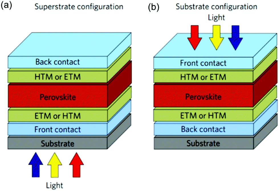 | ||
| Fig. 14 Scheme of a perovskite solar cell in the (a) conventional superstrate configuration and (b) the substrate configuration.67 | ||
Mathews and coworkers used triple cation perovskite to demonstrate a 16% efficiency ST-PSCs, which had an average transmittance of 12% in the visible region and >50% in the NIR region, respectively. They observed that the Ag buffer layer improved the adhesion to the underlayer and FF, outcompeting the MoOx buffer layer. They demonstrated a 20.7% efficiency for 4-T tandem based on the ST-PSCs and CIGS (unfiltered: 12.3%, filtered: 4.7%).70 Catchpole and coworkers engineered the perovskite composition: FA is the primary cation (75%) due to its stability towards moisture and heat; 15% MA can reduce the size discrepancy of FA and Cs, reduce defects, and facilitate the formation of α-phase perovskite. Cs can inhibit humidity-induced decomposition and strain-induced phase segregation, remove the yellow phase, and improve device performance and stability. Rb can balance the tolerance factor, and enhance efficiency and stability. Consequently, they utilized the 1.62 eV Eg Cs0.05Rb0.05FA0.765MA0.135PbI2.55Br0.45 and developed a 18.1%-efficiency ST-PSC. The combination of ST-PSC and CIGS subcell (unfiltered: 16.5%, filtered: 5.8%) gave a 4-T tandem efficiency of 23.9%. They also delivered a 16.0% PCE ST-PSCs based on 1.75 eV Cs0.1Rb0.05FA0.75MA0.15PbI1.8Br1.2, and 23.4% 4-T perovskite–CIGS tandem based on 16.0%-efficiency ST-PSCs and CIGS. Besides, the four-cation perovskite absorbers exhibit less oxygen sensitivity than MAPbI3. They deduced that the interaction between MA and oxygen molecules increased surface recombination, resulting in oxygen-induced degradation.
For perovskite–CIGS 4-T tandems, it is essential to reduce the defect density and increase the long lifetime of wide-Eg perovskite films. In 2015, Tiwari and coworkers updated the performance of perovskite–CIGS 4-T tandems through concerted efforts.68 On the one hand, PCBM was incorporated into the regular device structure, enabled by a hybrid thermal evaporation-spin coating technique. PCBM facilitated the growth of high-quality perovskite absorbers and inhibited hysteresis. Fig. 15a and b presents the cross-sectional SEM images of the planar PSCs with and without the PCBM layer, respectively. The perovskite layer on ZnO exhibits considerable surface roughness and thickness non-uniformity. When grown on PCBM, a uniform and compact perovskite layer with a large grain size can be obtained. As Fig. 15c and d shows, the device with a PCBM layer exhibits a PCE of 14.5%, together with a VOC of 1.101 V, JSC of 17.6 mA cm−2, and FF of 74.9%. On the other hand, sputtered In2O3:H is employed as a transparent rear electrode, yielding 14.2% steady-state efficiency, and 72% average transmittance between 800 and 1150 nm (Fig. 15e and f). Furthermore, they demonstrated 20.5% efficiency for the 4-T perovskite–CIGS (unfiltered: 18.3%; filtered: 6.3%) tandem configuration. Via the 2D–3D heterostructure strategy, Zhu and coworkers from the NERL demonstrated ∼20%-efficiency opaque PSCs by incorporating PEAI and Pb(SCN)2 binary additives in the FA0.65MA0.20Cs0.15PbI2.4I0.6 precursor.71 These additives form a quasi-2D phase located primarily at grain boundaries. The synergy of PEA+ and SCN− overcame the separate challenges of each additive, enhanced perovskite morphology, inhibited PbI2 formation (compared with the sole addition of Pb(SCN)2), and reduced defect density and energetic disorder. The coupling of a 1.68 eV ST-PSC (17.1% efficiency) and a 1.12 eV CIGS bottom cell (unfiltered: 20.7%; filtered: 8.8%) afforded a record-high 25.9%-efficiency 4-T polycrystalline perovskite–CIGS 4-T TSCs.
 | ||
| Fig. 15 The cross-sectional SEM images of devices without (a) and with (b) PCBM, respectively. The current density–voltage (J–V) curves (c) and EQE spectra (d) of the planar perovskite solar cells. The current density–voltage (J–V) curves (e) and EQE spectra (f) of the four-terminal perovskite–CIGS tandem device.68 | ||
Segawa and coworkers achieved a high PCE of 28% in a perovskite–CIGS 4-T tandem comprising a perovskite top cell and a CIGS bottom cell with Eg of 1.59 and 1.02 eV, based on a spectrum splitting system equipped with a dichroic mirror with splitting wavelengths of 775 nm. Tandem devices using perovskite and CIGS can potentially exhibit high flexibilities, which cannot be achieved with Si cells. Spectrum splitting tandem cells may not be ideal for practical applications. Nonetheless, this study shows experimentally that perovskite–CIGS TSCs are not only mechanically superior but also exhibit a higher efficiency than Si-based TSCs.72,73
4.2 Perovskite–CIGS 2-T TSCs
Different from other tandems, only p–i–n PSCs can work as top cells for perovskite–CIGS 2-T tandems, as the bottom CIGS cell has a typical structure of a glass/Mo/p-CIGS/n-CdS/ZnO structure. In 2015, Guha and coworkers realized monolithic 2-T perovskite–CIGS tandems, where both subcells are customized (Fig. 16).69 The Eg of CIGS was narrowed from 1.1 eV to 1.04 eV. The optical properties of perovskite were controlled by vapor-based halide exchange reactions. They designed a reactor for continuous in situ monitoring and precise control of perovskite's Egvia vapor-based halide exchange reactions (Fig. 16a). The sample of spin-coated PbI2 was annealed by the excess solid MAI vapor source until the layer is converted to 1.58 eV perovskite. MAI can be replaced with MABr. With continued annealing, the Eg will increase when I is replaced by Br, and the samples exhibited different Eg values: 1.65 eV (B2), 1.72 eV (B3), and 1.75 eV (B4). In a reverse-sequence process, the Eg of a pure bromide perovskite (C1 with 2.29 eV Eg) is reduced to the following values of 1.95 eV (C2), 1.86 eV(C3), and 1.7 eV (C4) with the MAI vapor (Fig. 16b and c). Consequently, a PCE of 10.9% was obtained for a monolithic 2-T perovskite–CIGS tandem cell (Fig. 16d).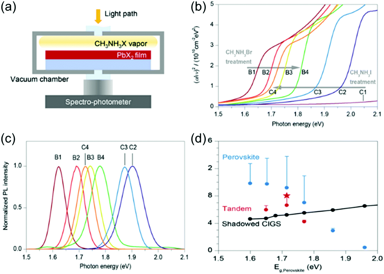 | ||
| Fig. 16 (a) Scheme of in situ bandgap tuning apparatus. (b) Tauc plots of sample series B and C, showing a blueshift progression with CH3NH3Br vapor treatment and a redshift progression with CH3NH3I vapor treatment, respectively. (c) PL spectra of series B and C. (d) Efficiency plotted against the bandgap of perovskite.69 | ||
Besides, CIGS has a very rough surface due to the common vacuum fabrication (sputtering and co-evaporation), which is problematic for building a smooth ICL atop it and may cause the failure of PSCs. Albrecht and coworkers introduced two new hole-selective contacts (MeO-2PACz and 2PACz) for p–i–n PSCs.74 These two molecules feature carbazole blocks with phosphonic acid anchoring groups, which enabled the formation of self-assembled monolayers (SAMS) on various oxides, which is ordered and stabilized by π–π interactions between adjacent carbazole fragments. These two SAMS exhibit weaker absorption in the visible wavelength compared with the PTAA interlayer and have an energy alignment to the perovskite absorber. The MeO-2PACz SAM layer enabled dopant-, additive- and interlayer-free PSCs with stabilized PCEs of up to 21.1%, and allowed the realization of a monolithic 2-T CIGSe/perovskite TSC with a certified PCE of 23.26%. The simplicity and diverse substrate compatibility of SAMs help ease the fabrication of 2-T CIGSe/perovskite TSC. Yang and coworkers designed a 22.43% efficiency 2-T perovskite–CIGS tandem with an architecture of Glass/Mo/CIGS/CdS/i-ZnO/boron-doped ZnO (BZO)/ITO/PTAA/Perovskite-PCBM/ZnO NPs/ITO/MgF2. They carried out nanoscale interface engineering of the CIGS surface and used a heavily doped PTAA HTL between two subcells that preserved VOC and enhanced FF and JSC.75 They first deposited an ITO layer and then used chemical mechanical polishing to smooth out the ITO surface. The polishing process reduced the vertical distance of ITO to 40 nm. Note, that the BZO layer under the ITO was not polished, and the original CIGS solar cell can be retained. As the BZO layer displayed a much lower work function (4.0 eV) than PTAA (5.1 eV), the ITO between BZO and PTAA created better ohmic contact. A monolithic 2-T perovskite–CIGS TSC achieved a 22.43% efficiency, and the unencapsulated devices in air retained 88% of their initial efficiency after 500 hours of aging under continuous 1 sun illumination.
4.3 Perovskite–CZTSSe TSCs
Compared with CIGS, Cu2ZnSn(S,Se)4 (CZTSSe) does not use rare metal elements, In and Ga, and thus has a low cost. CZTSSe has a high absorption coefficient of >104 cm−1 in the visible wavelengths and a high theoretical PCE of 28%. The Eg of CZTSSe can vary from 1.00 to 1.50 eV, which is mainly tuned by the ratio of S/Se.Guha and coworkers demonstrated a monolithic 2-T tandem cell with solution-processed kesterite CZTSSe and MAPbI3. The device exhibited a high VOC of 1.353 V, close to the sum VOC of the single-junction subcells. The 2-T tandem exhibited a very disappointing PCE of 4.6%, compared with 11.6% for CZTSSe and 12.3% for MAPbI3.76 Although other factors to the high Rs (15.7 Ω cm2) cannot be ruled out, the drastically reduced illumination in all layers and high Rs of the Al contact are major contributors to the low JSC and FF. Ding and coworkers present a tandem combining solution-processed perovskite and CZTSSe subcells in a reflective configuration.77 The 1.70 eV-Eg perovskite subcell acts as a spectral filter reflecting the sub-bandgap photons to a low bandgap CZTSSe cell. A 4-T measurement afforded a sum efficiency of 16.1%, showing the potential of perovskite–CZTSSe 4-T tandems in realizing high performance and low fabrication cost simultaneously.
5. Perovskite–organic TSCs
Organic solar cells (OSCs) are another emerging PV technology.78,79 OSCs can be fabricated through low-cost solution processes using environmentally friendly materials. OSCs can be made into lightweight, flexible, and semi-transparent devices. Currently, OSCs have achieved up to 18.2% certified PCE.80 Perovskite and organic semiconductors have composition and molecular tunability to enable a large pool of photoactive material with different optoelectronic properties, offering the feasibility to construct high-performance perovskite–organic TSCs.5.1 Perovskite–organic 4-T TSCs
Hygroscopicity risk and easy decomposition are the obvious drawbacks of organic–inorganic hybrid perovskites. Compared with the hybrid organic–inorganic perovskites, all-inorganic perovskite solar cells display better stability toward moisture, light soaking, and thermal stressing.81,82 In particular, CsPbI3 perovskite with Eg of 1.73 eV can serve as a top cell in tandem devices with silicon solar cells. CsPbI3 also exhibits good thermal stability. However, it is difficult to maintain the bandgap and phase stability of CsPbI3, due to their low tolerance factor, the large crystal distortion, and moisture. The all-inorganic perovskite CsPbBr3 has demonstrated the most promising stability against heat and humidity. For instance, the CsPbBr3-based mesoporous PSCs displayed minimal performance degradation when exposed to highly humid air and extreme temperatures for longer than 3 months. CsPbBr3 presents a wide Eg of ≈2.3 eV, efficiently harvests short-wavelength sunlight in the 300–530 nm wavelength range, and can achieve ≈90% EQE at the wavelength ≈400 nm. Generally, a high VOC of ≈1.25 V and high transmittance in the visible region at wavelengths >530 nm can be afforded by mesoporous CsPbBr3 PSCs, indicating the potential of CsPbBr3 in the ST device and TSCs. Li and coworkers addressed OSCs' photostability issue without efficiency loss by constructing CsPbBr3/organic 4-T TSCs. They prepared high-quality CsPbBr3 all-inorganic perovskite films with a low defect concentration using the dual-source vacuum thermal evaporation method. The corresponding CsPbBr3 film displays a high AVT of 90.9% in the 530–800 nm wavelength range. The opaque planar PSC exhibited a VOC of 1.44 V, a PCE of 7.78%, and good UV stability. The semitransparent PSC with the transfer-laminated PH1000 anode showed a PCE of 5.98% with a JSC of 6.15 mA cm−2, a VOC of 1.38 V, and an FF of 70.51%. The perovskite ST devices were paired with PTB7-Th:PC71BM (unfiltered: 9.06%, filtered: 4.63%), PBDB-T:ITIC (unfiltered: 10.10%, filtered: 5.59%) and PBDB-T-SF:IT-4F (unfiltered: 13.72%, filtered: 8.05%) systems, to deliver a sum PCE of 10.61%, 11.57%, and 14.03%, respectively. These tandems exhibit good UV stability, which is reflected in the fact that they reserve 97.3–99.4% of the initial PCEs after 100 mW cm−2 for 120 h.835.2 Perovskite–organic 2-T TSCs
The study of perovskite–organic TSCs was pioneered by thre Yang group in 2015. In their work, MAPbI3 was processed via a one-step deposition with a small-molecule additive named BmPyPhB, which provided heterogeneous nucleation sites and improved the uniformity of the initial nucleation process of perovskite crystals. The organic system (PBSeDTEG8:PCBM) exhibited photosensitivity up to 950 nm and good thermal stability to endure PSC's thermal annealing process. The monolithic 2-T perovskite–organic tandem cells exhibit an efficiency of 10.2%.84The Jen group demonstrated unique semi-transparent monolithic 2-T TSCs by rationally choosing selective absorbing photoactive materials.85 They developed 2.36 eV-Eg FAPbBr2.43Cl0.57 perovskite with efficient selective absorption in the UV region and meanwhile utilized an organic BHJ blend of PTB7-Th:6TIC-4F with an absorption onset at ≈980 nm (Fig. 17a). Therefore, the balance of energy loss between thermalization and transmission is improved, and the resulting 2-T S-T TSC delivered a PCE of 10.7%, an averaged transmittance of 52.91%, and a light utilization efficiency of 5.66% (Fig. 17b). The Jen group further employed phenmethylammonium bromide (PMABr) to passivate the wide-Eg perovskite Cs0.1(FA0.6MA0.4)0.9Pb(I0.6Br0.4)3 and obtain a high VOC of 1.22 V for the PSC.86 The assembled rigid perovskite–organic 2-T TSCs yielded a remarkable PCE of 15.13%, with VOC of 1.85 V, JSC of 11.52 mA cm−2, and FF of 70.98%. Moreover, they realized flexible perovskite–organic TSCs with a PCE of 13.61% and a VOC of 1.80 V. The rigid and flexible perovskite–organic TSC generated a solar-to-hydrogen efficiency of 12.30% and 11.21%, illustrating the potential application of perovskite–organic TSCs in a photovoltaics-driven water splitting system. Zeng et al. demonstrated all-inorganic perovskite–organic TSCs with a CsPbI2Br cell as the front cell and PTB7-Th:COi8DFIC:PC71BM as the rear cell. The wide-Eg CsPbI2Br can absorb short-wavelength photons before 650 nm, while the low-bandgap NFA COi8DFIC can absorb long-wavelength photons until 1050 nm. They uses a device structure of ITO/SnO2/CsPbI2Br/PTAA/ICL/ZnO/PTB7-Th:COi8DFIC:PC71BM/MoO3/Ag, where the ICL consisting of MoO3/Au was made by thermal deposition. The corresponding best tandem exhibits a PCE of 15.04%, with a VOC of 1.71 V, a JSC of 11.98 mA cm−2, and an FF of 73.4%.87 Very recently, Chen et al. developed a semi-empirical model to calculate the practical PCE limits of perovskite–organic TSCs. Based on their calculation, an efficiency >30% is approachable with the rapid advances of low-Eg organic semiconductors and wide-Eg perovskite materials. They prepared monolithic perovskite–organic TSCs by employing a 1.77 eV-Eg FA0.8MA0.02Cs0.18PbI1.8Br1.2 for the front cell and a 1.41 eV-Eg organic material for the rear subcell (Fig. 18a).88 As shown in Fig. 18b, the absorbed energy distribution is simulated by the transfer matrix method. To effectively match the JSC, they established the relationship between the photo-current and the thickness of each subcell. The highlighted blue curve indicates that the JSC of both subcells is matched theoretically (Fig. 18d). Featuring all-thermally evaporated BCP/Ag/MoO3 ICLs, the 2-T monolithic perovskite–organic tandems delivered good reproducibility and a landmark PCE of 20.6% (certified as 19.54%). The UV sensitivity of OPVs is significantly reduced with the UV filtering function of the perovskite layer. Recently, the integrated perovskite–organic solar cells without any recombination layers have generated wide attention. This integrated structure takes the advantages of tandem cells using both perovskite solar cells and NIR BHJ organic solar cells for wide-range absorption and the simple fabrication of a single-junction device.89–91 The high VOC and wide-range absorption can be maintained at the same time. However, as this device does not belong to the tandem device in the strict sense, it will not be discussed here.
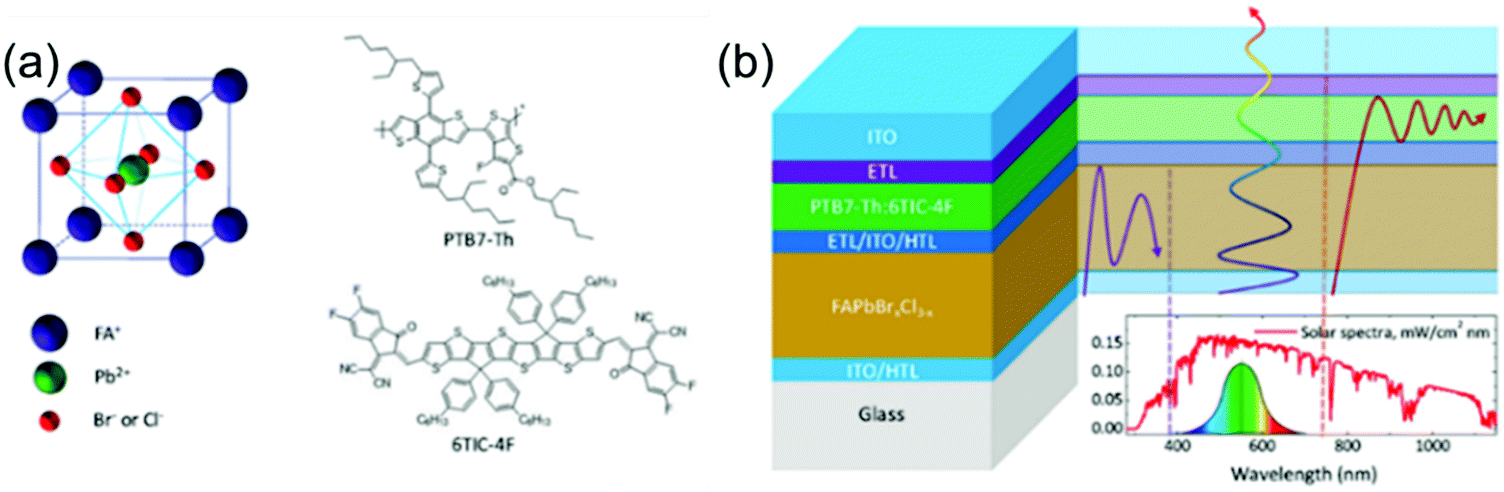 | ||
| Fig. 17 (a) Scheme of FAPbBrxCl3−x perovskite crystal lattice, Chemical structures of PTB7-Th and 6TIC-4F. (b) Device architectures of selective absorbing tandem ST-PVs.85 | ||
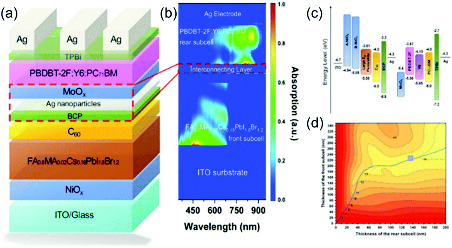 | ||
| Fig. 18 (a) Perovskite–organic tandem structure with an ICL of MoOx/Ag nanoparticles/BCP. (b) The simulation of the photon absorption distribution in tandem. (c) Energy level distribution of the components in the tandem device. (d) Stimulated current density as a function of the thicknesses of the front and rear subcells.88 | ||
Conclusions and outlook
Perovskite solar cells are an ideal candidate to construct tandem cells, due to their high VOC, highly tunable Eg, and low-temperature solution processability. We have presented the key advances of perovskite–silicon, all-perovskite, perovskite–CIGS, and perovskite–organic TSCs. Currently, the 1 cm2 perovskite–silicon monolithic two-junction, the two-terminal device has achieved the highest results of 29.15%, which pushes further beyond the highest efficiency for a single-junction silicon cell with a 9% relative advantage. Perovskite TSCs are stepping towards commercialization, which requires high device efficiencies, long-term stability, and low-cost and reproducible fabrication. The following challenges and strategies should be considered for future developments.The high-performing tandems required reduced additional optical losses (reflective losses and parasitic absorption losses) and electrical losses in a tandem structure. The optical losses of PSCs are greatly reduced by changing the configuration of PSCs from n–i–p to p–i–n, which may account for the phenomenon that the maximum efficiency of TSCs is obtained with p–i–n PSCs. The parasitic absorption in p–i–n PSCs can be minimized by reducing the thickness of the electron transport layer like C60 and PCBM, where the following wide-bandgap BCP/Bphen layer can work as the hole-blocking layer and the buffer layer. Take perovskite–Si TSCs as an example, PSCs with the p–i–n structure are the most promising for high PCEs due to the less optical losses, low cost, and compatible fabrication process with the SHJ structure.92
LM layers like MgF2 and SiOx on the substrate surface should be utilized to reduce the reflective optical loss. The transparent electrode should have high conductivity and high transparency. ICLs should have small resistance and lateral conductivity and high transparency. The high-performance tandems also require efficient subcells.
(1) Wide-bandgap PSCs
Compositional engineering, the partial substitution of I by Br for instance, can enlarge the bandgap of perovskite. The quality of wide-bandgap perovskite film should be improved, with low defect concentration, weak charge recombination, and long carrier lifetime. As discussed above, many strategies are reported, such as the incorporation of Gua/PEA-based additives for constructing the 2D–3D hybrid structure, Lewis bases/acids, PbI2, Br and Cl, ligand passivation, and metal ions. To fabricate PSCs on the textured or rough surfaces of Si and CIG solar cells, some special fabrication methods should be utilized, like blade-coating, thermal co-evaporation, and the vacuum-solution binary step.(2) Narrow-bandgap bottom cells
The Sn–Pb PSCs should be improved by tackling the material and device issues. First, Sn and Sn–Pb perovskites require thick film perovskite absorbers and in turn long carrier diffusion lengths. Second, the quick crystallization of Sn-substituted perovskite results in inferior-quality films. Last, the facile oxidation of Sn2+ to Sn4+ degrades its device performance. Several strategies are reported and summarized in the manuscript, which is partially similar to the strategies for wide-Eg perovskites, such as the addition of Cl, excess metal ions, SnI2, SnF2, SnCl2, FA, Cd, insulating polymers, and alkali metal ions. For organic bottom cells, high-performance non-fullerene acceptors, especially fused-ring electron acceptors, should be developed. The match of donors and acceptors should be guaranteed. The ternary/multiple strategies can be applied. The bulk-heterojunction active layer should be optimized by device engineering, including solvent additive, thermal annealing, and solvent vapor annealing. As Si and CIG bottom cells already have very mature products, their improvement is not the highlight to some extent. The bandgap and thickness of the top and bottom cells should be prudently optimized together.To reduce the cell-to-module PCE gap, the main step is to obtain high-performance large-scale perovskite top cells. Our group recently performed systematic investigations on fabricating PSCs via blade coating under ambient conditions with high humidity and room temperature. The morphological and photoluminescence characterization indicate that air-knife-assisted drying significantly contributed to nucleation of the perovskite, determination of the thin-film morphology and device performance, and protection of the perovskite and its intermediate phase against moisture during solidification. We fabricated hysteresis-free PSCs with a PCE of 21.1% and 18.0% for small and large-area blade-coated devices, comparable to that of the glovebox-processed blade-coated device. These PSCs also exhibit comparable stability to those fabricated in a glovebox. Our group also induces a multifunctional sulfobetaine-based zwitterionic surfactant to facilitate room-temperature meniscus coating of high-quality perovskite films. The systematic in situ study revealed the crystallization pathway of perovskite and emphasized the synergistic effects of surfactants in film formation, crystallization kinetics adjustment, defect passivation, and moisture barrier protection. The coated PSCs have negligible deterioration when the device area is upscaled to 0.8 cm2, which is among the highest records for the upscaling coated PSCs. Besides, this method significantly improves the stability of perovskite films and devices under different aging conditions.93–95 However, it is still challenging to deposit sub-μm thick perovskite layers from solution onto textured silicon with typical pyramids of 3–10 μm height. The Huang group demonstrated a new perovskite/silicon tandem solar cell architecture involving silicon wafers textured with pyramids less than 1 μm in height, which are rough enough to scatter light within the silicon but smooth enough to solution process a perovskite film. The silicon bottom cell was fully textured with scalable chemistries. The sub-μm pyramids and precursor additives enabled solution-processed dense perovskite layers that fully cover the silicon texture. This tandem architecture can be adopted by silicon solar cell manufacturers, which hunt for tandem technologies with low required capital expenditures, the potential for rapid scaling, and minimum modification of their silicon cells.
For perovskite–organic tandems, large-scale fabrication also imposes requirements of large-scale OSCs. Orthogonal solvents should be used to protect the layers underneath. Otherwise, barrier layers should be designed, or a vacuum-deposition method should be utilized. Optimization of interconnection design to achieve a right balance between leakage currents and resistive losses is also indispensable for large-scale fabrication.
Stability is another essential factor for the commercialization of perovskite TSCs. For instance, the stability of perovskite–Si tandems should match the 25 year lifetime of silicon solar cells. The polycrystalline perovskite films contain a high density of defects, including point and extended imperfections, which heavily influences the devices' stability. In terms of perovskite composition (ABX3), the X site poses photo-instability concerns; the A-site cation has a relationship with thermal, moisture, and oxygen instability. The volatile MA needs encapsulation to prevent volatilization. Besides, the narrow Eg perovskite with Sn2+ on the B-site has a strong tendency from the Sn2+ to Sn4+ state when exposed to oxygen or moisture. The A-site and X-site cations of perovskite are very mobile, which can also degrade stability. Photo-induced phase segregation in wide-Eg perovskite and the oxidation of Sn2+ to Sn4+ in low-bandgap are the main factors to limit the stability of PSC tandems. Admittedly, some strategies can use coordinate and ionic bonding to target the defects of the surface and grain boundaries, the conversion of those extended defects to wide Eg materials, and ion migration.96–100 For example, our group introduced NFA molecules (IT-M) as a Lewis base to improve perovskite interfaces, which effectively enhances the electronic properties of Cs0.05(MA0.17FA0.83)0.95Pb(I0.83Br0.17)3 thin films, passivates the perovskite surface defects, and further boosts the performance of PSCs. The introduction of IT-M significantly enhances the charge transport properties and boosts the photogenerated photoluminescence lifetime from 1.46 to 2.20 ms. Our group also found that the π-conjugated polymer PBDB-T triggers heterogeneous nucleation over the perovskite precursor film and passivates the trap states of the mixed perovskite through the formation of Lewis adducts between lead and oxygen atoms in PBDB-T. The p-type hydrophobic PBDB-T fills in the perovskite grain boundaries to improve charge transfer for better conductivity and prevent moisture invasion into the perovskite active layers, thus simultaneously improving efficiency and stability. However, it is still unexplored whether the phase segregation and the oxidation issues will reappear in the long term and how long the effects of the abovementioned strategies can last. Besides, the weak layer to layer adhesivity and different thermal expansion coefficients also deteriorate the perovskite tandems' long-term stability. Currently, there are no standards of stability measurements for scientific research. The literature involving the stability of PSC tandems has different test conditions, increasing the difficulty for scientists to compare the effectiveness of different stability strategies.
Overall, through concerted efforts of materials design, device engineering, interface engineering, device physics, and improved fabrication technology and encapsulation, perovskite tandems can overcome the abovementioned challenge. Ideal perovskite-based tandem cells, especially the perovskite–silicon tandem cell, can surpass 30% efficiency and achieve good stability, to meet commercialization requirements in the near future.
Conflicts of interest
There are no conflicts to declare.Acknowledgements
C. Yan and J. Huang contributed equally to this work. G. Li acknowledges the support from Research Grants Council of Hong Kong (Project No. 15218517, C5037-18G), Shenzhen Science and Technology Innovation Commission (Project No. JCYJ20170413154602102), and the funding for Project of Strategic Importance (Project Code: 1-ZE29), Sir Sze-yuen Chung Endowed Professorship (8-8480), and HK PolyU Postdoctoral Fellowships Scheme (YW3Y).Notes and references
- H. L. Hu, M. Singh, X. J. Wan, J. N. Tang, C. W. Chu and G. Li, Nucleation and crystal growth control for scalable solution-processed organic-inorganic hybrid perovskite solar cells, J. Mater. Chem. A, 2020, 8, 1578–1603 RSC.
- A. Kojima, K. Teshima, Y. Shirai and T. Miyasaka, Organometal halide perovskites as visible-light sensitizers for photovoltaic cells, J. Am. Chem. Soc., 2009, 131, 6050–6051 CrossRef CAS PubMed.
- M. Liu, M. B. Johnston and H. J. Snaith, Efficient planar heterojunction perovskite solar cells by vapour deposition, Nature, 2013, 501, 395–398 CrossRef CAS PubMed.
- N. Arora, M. I. Dar, A. Hinderhofer, N. Pellet, F. Schreiber, S. M. Zakeeruddin and M. Grätzel, Perovskite solar cells with CuSCN hole extraction layers yield stabilized efficiencies greater than 20%, Science, 2017, 358, 768–771 CrossRef CAS PubMed.
- Q. Jiang, Y. Zhao, X. Zhang, X. Yang, Y. Chen, Z. Chu, Q. Ye, X. Li, Z. Yin and J. You, Surface passivation of perovskite film for efficient solar cells, Nat. Photon., 2019, 13, 460–466 CrossRef CAS.
- W. Shockley and H. J. Queisser, Detailed balance limit of efficiency of p–n junction solar cells, J. Appl. Phys., 1961, 32, 510–519 CrossRef CAS.
- M. A. Green, E. D. Dunlop, J. Hohl-Ebinger, M. Yoshita, N. Kopidakis and A. W. Y. Ho-Baillie, Solar cell efficiency tables (Version 55), Prog. Photovoltaics, 2020, 28, 3–15 Search PubMed.
- K. Yoshikawa, H. Kawasaki, W. Yoshida, T. Irie, K. Konishi, K. Nakano, T. Uto, D. Adachi, M. Kanematsu, H. Uzu and K. Yamamoto, Silicon heterojunction solar cell with interdigitated back contacts for a photoconversion efficiency over 26%, Nat. Energy, 2017, 2, 17032 CrossRef CAS.
- P. Loper, S. J. Moon, S. M. de Nicolas, B. Niesen, M. Ledinsky, S. Nicolay, J. Bailat, J. H. Yum, S. De Wolf and C. Ballif, Organic–inorganic halide perovskite/crystalline silicon four-terminal tandem solar cells, Phys. Chem. Chem. Phys., 2015, 17, 1619–1629 RSC.
- K. A. Bush, C. D. Bailie, Y. Chen, A. R. Bowring, W. Wang, W. Ma, T. Leijtens, F. Moghadam and M. D. McGehee, Thermal and environmental stability of semi-transparent perovskite solar cells for tandems enabled by a solution-processed nanoparticle buffer layer and sputtered ITO electrode, Adv. Mater., 2016, 28, 3937–3943 CrossRef CAS PubMed.
- J. Werner, G. Dubuis, A. Walter, P. Löper, S.-J. Moon, S. Nicolay, M. Morales-Masis, S. De Wolf, B. Niesen and C. Ballif, Sputtered rear electrode with broadband transparency for perovskite solar cells, Sol. Energy Mater. Sol. Cells, 2015, 141, 407–413 CrossRef CAS.
- B. Chen, S.-W. Baek, Y. Hou, E. Aydin, M. De Bastiani, B. Scheffel, A. Proppe, Z. Huang, M. Wei, Y.-K. Wang, E.-H. Jung, T. G. Allen, E. Van Kerschaver, F. P. García De Arquer, M. I. Saidaminov, S. Hoogland, S. De Wolf and E. H. Sargent, Enhanced optical path and electron diffusion length enable high-efficiency perovskite tandems, Nat. Commun., 2020, 11, 1257 CrossRef CAS PubMed.
- G. E. Eperon, V. M. Burlakov, A. Goriely and H. J. Snaith, Neutral color semitransparent microstructured perovskite solar cells, ACS Nano, 2014, 8, 591–598 CrossRef CAS PubMed.
- E. Della Gaspera, Y. Peng, Q. Hou, L. Spiccia, U. Bach, J. J. Jasieniak and Y.-B. Cheng, Ultra-thin high efficiency semitransparent perovskite solar cells, Nano Energy, 2015, 13, 249–257 CrossRef CAS.
- Y. Yang, Q. Chen, Y.-T. Hsieh, T.-B. Song, N. D. Marco, H. Zhou and Y. Yang, Multilayer transparent top electrode for solution processed perovskite/Cu(In,Ga)(Se,S)2 four terminal tandem solar cells, ACS Nano, 2015, 9, 7714–7721 CrossRef CAS PubMed.
- B. Chen, Y. Bai, Z. Yu, T. Li, X. Zheng, Q. Dong, L. Shen, M. Boccard, A. Gruverman, Z. Holman and J. Huang, Efficient semitransparent perovskite solar cells for 23.0%-efficiency perovskite/silicon four-terminal tandem cells, Adv. Energy Mater., 2016, 6, 1601128 CrossRef.
- C. D. Bailie, M. G. Christoforo, J. P. Mailoa, A. R. Bowring, E. L. Unger, W. H. Nguyen, J. Burschka, N. Pellet, J. Z. Lee, M. Grätzel, R. Noufi, T. Buonassisi, A. Salleo and M. D. McGehee, Semi-transparent perovskite solar cells for tandems with silicon and CIGS, Energy Environ. Sci., 2015, 8, 956–963 RSC.
- Z. Wang, X. Zhu, S. Zuo, M. Chen, C. Zhang, C. Wang, X. Ren, Z. Yang, Z. Liu, X. Xu, Q. Chang, S. Yang, F. Meng, Z. Liu, N. Yuan, J. Ding, S. Liu and D. Yang, 27%-Efficiency four-terminal perovskite/silicon tandem solar cells by sandwiched gold nanomesh, Adv. Funct. Mater., 2020, 30, 1908298 CrossRef CAS.
- F. Lang, M. A. Gluba, S. Albrecht, J. Rappich, L. Korte, B. Rech and N. H. Nickel, Perovskite solar cells with large-area CVD-graphene for tandem solar cells, J. Phys. Chem. Lett., 2015, 6, 2745–2750 CrossRef CAS PubMed.
- P. You, Z. Liu, Q. Tai, S. Liu and F. Yan, Efficient semitransparent perovskite solar cells with graphene electrodes, Adv. Mater., 2015, 27, 3632–3638 CrossRef CAS PubMed.
- M. Jaysankar, M. Filipič, B. Zielinski, R. Schmager, W. Song, W. Qiu, U. W. Paetzold, T. Aernouts, M. Debucquoy, R. Gehlhaar and J. Poortmans, Perovskite–silicon tandem solar modules with optimised light harvesting, Energy Environ. Sci., 2018, 11, 1489–1498 RSC.
- H. Uzu, M. Ichikawa, M. Hino, K. Nakano, T. Meguro, J. L. Hernández, H.-S. Kim, N.-G. Park and K. Yamamoto, High efficiency solar cells combining a perovskite and a silicon heterojunction solar cells via an optical splitting system, Appl. Phys. Lett., 2015, 106, 013506 CrossRef.
- J. P. Mailoa, C. D. Bailie, E. C. Johlin, E. T. Hoke, A. J. Akey, W. H. Nguyen, M. D. McGehee and T. Buonassisi, A 2-terminal perovskite/silicon multijunction solar cell enabled by a silicon tunnel junction, Appl. Phys. Lett., 2015, 106, 121105 CrossRef.
- S. Albrecht, M. Saliba, J. P. Correa Baena, F. Lang, L. Kegelmann, M. Mews, L. Steier, A. Abate, J. Rappich, L. Korte, R. Schlatmann, M. K. Nazeeruddin, A. Hagfeldt, M. Grätzel and B. Rech, Monolithic perovskite/silicon-heterojunction tandem solar cells processed at low temperature, Energy Environ. Sci., 2016, 9, 81–88 RSC.
- J. Werner, C.-H. Weng, A. Walter, L. Fesquet, J. P. Seif, S. De Wolf, B. Niesen and C. Ballif, Efficient monolithic perovskite/silicon tandem solar cell with cell area >1 cm2, J. Phys. Chem. Lett., 2016, 7, 161–166 CrossRef CAS PubMed.
- J. Zheng, C. F. J. Lau, H. Mehrvarz, F.-J. Ma, Y. Jiang, X. Deng, A. Soeriyadi, J. Kim, M. Zhang, L. Hu, X. Cui, D. S. Lee, J. Bing, Y. Cho, C. Chen, M. A. Green, S. Huang and A. W. Y. Ho-Baillie, Large area efficient interface layer free monolithic perovskite/homo-junction-silicon tandem solar cell with over 20% efficiency, Energy Environ. Sci., 2018, 11, 2432–2443 RSC.
- J. Zheng, H. Mehrvarz, F.-J. Ma, C. F. J. Lau, M. A. Green, S. Huang and A. W. Y. Ho-Baillie, 21.8% Efficient monolithic perovskite/homo-junction-silicon tandem solar cell on 16 cm2, ACS Energy Lett., 2018, 3, 2299–2300 CrossRef CAS.
- J. Zheng, H. Mehrvarz, C. Liao, J. Bing, X. Cui, Y. Li, V. R. Gonçales, C. F. J. Lau, D. S. Lee, Y. Li, M. Zhang, J. Kim, Y. Cho, L. G. Caro, S. Tang, C. Chen, S. Huang and A. W. Y. Ho-Baillie, Large-area 23%-efficient monolithic perovskite/homojunction-silicon tandem solar cell with enhanced UV stability using down-shifting material, ACS Energy Lett., 2019, 4, 2623–2631 CrossRef CAS.
- H. Shen, S. T. Omelchenko, D. A. Jacobs, S. Yalamanchili, Y. Wan, D. Yan, P. Phang, T. Duong, Y. Wu, Y. Yin, C. Samundsett, J. Peng, N. Wu, T. P. White, G. G. Andersson, N. S. Lewis and K. R. Catchpole, In situ recombination junction between p-Si and TiO2 enables high-efficiency monolithic perovskite/Si tandem cells, Sci. Adv., 2018, 4, eaau9711 CrossRef CAS PubMed.
- M. Jošt, E. Köhnen, A. B. Morales-Vilches, B. Lipovšek, K. Jäger, B. Macco, A. Al-Ashouri, J. Krč, L. Korte, B. Rech, R. Schlatmann, M. Topič, B. Stannowski and S. Albrecht, Textured interfaces in monolithic perovskite/silicon tandem solar cells: Advanced light management for improved efficiency and energy yield, Energy Environ. Sci., 2018, 11, 3511–3523 RSC.
- L. Mazzarella, Y.-H. Lin, S. Kirner, A. B. Morales-Vilches, L. Korte, S. Albrecht, E. Crossland, B. Stannowski, C. Case, H. J. Snaith and R. Schlatmann, Infrared light management using a nanocrystalline silicon oxide interlayer in monolithic perovskite/silicon heterojunction tandem solar cells with efficiency above 25%, Adv. Energy Mater., 2019, 9, 1803241 CrossRef.
- Y. Hou, E. Aydin, M. De Bastiani, C. Xiao, F. H. Isikgor, D. J. Xue, B. Chen, H. Chen, B. Bahrami, A. H. Chowdhury, A. Johnston, S. W. Baek, Z. Huang, M. Wei, Y. Dong, J. Troughton, R. Jalmood, A. J. Mirabelli, T. G. Allen, E. Van Kerschaver, M. I. Saidaminov, D. Baran, Q. Qiao, K. Zhu, S. De Wolf and E. H. Sargent, Efficient tandem solar cells with solution-processed perovskite on textured crystalline silicon, Science, 2020, 367, 1135–1140 CrossRef CAS PubMed.
- B. Chen, Z. J. Yu, S. Manzoor, S. Wang, W. Weigand, Z. Yu, G. Yang, Z. Ni, X. Dai, Z. C. Holman and J. Huang, Blade-coated perovskites on textured silicon for 26%-efficient monolithic perovskite/silicon tandem solar cells, Joule, 2020, 4, 850–864 CrossRef CAS.
- A. Cuevas, A. Luque, J. Eguren and J. del Alamo, 50 Per cent more output power from an albedo-collecting flat panel using bifacial solar cells, Sol. Energy, 1982, 29, 419–420 CrossRef.
- T. C. R. Russell, R. Saive, A. Augusto, S. G. Bowden and H. A. Atwater, The influence of spectral Albedo on bifacial solar cells: A theoretical and experimental study, IEEE J. Photovolt., 2017, 7, 1611–1618 Search PubMed.
- G. Coletti, S. L. Luxembourg, L. J. Geerligs, V. Rosca, A. R. Burgers, Y. Wu, L. Okel, M. Kloos, F. J. K. Danzl, M. Najafi, D. Zhang, I. Dogan, V. Zardetto, F. Di Giacomo, J. Kroon, T. Aernouts, J. Hüpkes, C. H. Burgess, M. Creatore, R. Andriessen and S. Veenstra, Bifacial four-terminal perovskite/silicon tandem solar cells and modules, ACS Energy Lett., 2020, 5, 1676–1680 CrossRef CAS.
- A. Onno, N. Rodkey, A. Asgharzadeh, S. Manzoor, Z. S. J. Yu, F. Toor and Z. C. Holman, Predicted power output of silicon-based bifacial tandem photovoltaic systems, Joule, 2020, 4, 580–596 CrossRef CAS.
- O. Dupre, A. Tuomiranta, Q. Jeangros, M. Boccard, P. J. Alet and C. Ballif, Design rules to fully benefit from bifaciality in two-terminal perovskite/silicon tandem solar cells, IEEE J. Photovolt., 2020, 10, 714–721 Search PubMed.
- M. De Bastiani, A. J. Mirabelli, Y. Hou, F. Gota, E. Aydin, T. G. Allen, J. Troughton, A. S. Subbiah, F. H. Isikgor, J. Liu, L. J. Xu, B. Chen, E. Van Kerschaver, D. Baran, B. Fraboni, M. F. Salvador, U. W. Paetzold, E. H. Sargent and S. De Wolf, Efficient bifacial monolithic perovskite/silicon tandem solar cells via bandgap engineering, Nat. Energy, 2021, 6, 167–175 CrossRef CAS.
- T. Leijtens, K. A. Bush, R. Prasanna and M. D. McGehee, Opportunities and challenges for tandem solar cells using metal halide perovskite semiconductors, Nat. Energy, 2018, 3, 828–838 CrossRef CAS.
- E. T. Hoke, D. J. Slotcavage, E. R. Dohner, A. R. Bowring, H. I. Karunadasa and M. D. McGehee, Reversible photo-induced trap formation in mixed-halide hybrid perovskites for photovoltaics, Chem. Sci., 2015, 6, 613–617 RSC.
- Z. Qiu, Z. Xu, N. Li, N. Zhou, Y. Chen, X. Wan, J. Liu, N. Li, X. Hao, P. Bi, Q. Chen, B. Cao and H. Zhou, Monolithic perovskite/Si tandem solar cells exceeding 22% efficiency via optimizing top cell absorber, Nano Energy, 2018, 53, 798–807 CrossRef CAS.
- J. Xu, C. C. Boyd, Z. J. Yu, A. F. Palmstrom, D. J. Witter, B. W. Larson, R. M. France, J. Werner, S. P. Harvey, E. J. Wolf, W. Weigand, S. Manzoor, M. F. A. M. Van Hest, J. J. Berry, J. M. Luther, Z. C. Holman and M. D. McGehee, Triple-halide wide–band gap perovskites with suppressed phase segregation for efficient tandems, Science, 2020, 367, 1097–1104 CrossRef CAS PubMed.
- Z. Wang, Q. Lin, F. P. Chmiel, N. Sakai, L. M. Herz and H. J. Snaith, Efficient ambient-air-stable solar cells with 2D–3D heterostructured butylammonium-caesium-formamidinium lead halide perovskites, Nat. Energy, 2017, 2, 17135 CrossRef CAS.
- D. Kim, H. J. Jung, I. J. Park, B. W. Larson, S. P. Dunfield, C. Xiao, J. Kim, J. Tong, P. Boonmongkolras, S. G. Ji, F. Zhang, S. R. Pae, M. Kim, S. B. Kang, V. Dravid, J. J. Berry, J. Y. Kim, K. Zhu, D. H. Kim and B. Shin, Efficient, stable silicon tandem cells enabled by anion-engineered wide-bandgap perovskites, Science, 2020, 368, 155–160 CrossRef CAS PubMed.
- A. Al-Ashouri, E. Köhnen, B. Li, A. Magomedov, H. Hempel, P. Caprioglio, J. A. Márquez, A. B. Morales Vilches, E. Kasparavicius, J. A. Smith, N. Phung, D. Menzel, M. Grischek, L. Kegelmann, D. Skroblin, C. Gollwitzer, T. Malinauskas, M. Jošt, G. Matič, B. Rech, R. Schlatmann, M. Topič, L. Korte, A. Abate, B. Stannowski, D. Neher, M. Stolterfoht, T. Unold, V. Getautis and S. Albrecht, Monolithic perovskite/silicon tandem solar cell with >29% efficiency by enhanced hole extraction, Science, 2020, 370, 1300–1309 CrossRef CAS PubMed.
- I. J. Park, J. H. Park, S. G. Ji, M.-A. Park, J. H. Jang and J. Y. Kim, A three-terminal monolithic perovskite/Si tandem solar cell characterization platform, Joule, 2019, 3, 807–818 CrossRef CAS.
- M. T. Hörantner, T. Leijtens, M. E. Ziffer, G. E. Eperon, M. G. Christoforo, M. D. McGehee and H. J. Snaith, The potential of multijunction perovskite solar cells, ACS Energy Lett., 2017, 2, 2506–2513 CrossRef.
- J. Werner, F. Sahli, F. Fu, J. J. Diaz Leon, A. Walter, B. A. Kamino, B. Niesen, S. Nicolay, Q. Jeangros and C. Ballif, Perovskite/perovskite/silicon monolithic triple-junction solar cells with a fully textured design, ACS Energy Lett., 2018, 3, 2052–2058 CrossRef CAS.
- F. Y. Jiang, T. F. Liu, B. W. Luo, J. H. Tong, F. Qin, S. X. Xiong, Z. F. Li and Y. H. Zhou, A two-terminal perovskite/perovskite tandem solar cell, J. Mater. Chem. A, 2016, 4, 1208–1213 RSC.
- J. H. Heo and S. H. Im, CH3NH3PbBr3–CH3NH3PbI3 perovskite–perovskite tandem solar cells with exceeding 2.2 V open circuit voltage, Adv. Mater., 2016, 28, 5121–5125 CrossRef CAS PubMed.
- Z. Chen, J. J. Wang, Y. Ren, C. Yu and K. Shum, Schottky solar cells based on CsSnI3 thin-films, Appl. Phys. Lett., 2012, 101, 093901 CrossRef.
- F. Hao, C. C. Stoumpos, R. P. H. Chang and M. G. Kanatzidis, Anomalous band gap behavior in mixed Sn and Pb perovskites enables broadening of absorption spectrum in solar cells, J. Am. Chem. Soc., 2014, 136, 8094–8099 CrossRef CAS PubMed.
- Y. Li, W. Sun, W. Yan, S. Ye, H. Rao, H. Peng, Z. Zhao, Z. Bian, Z. Liu, H. Zhou and C. Huang, 50% Sn-Based planar perovskite solar cell with power conversion efficiency up to 13.6%, Adv. Energy Mater., 2016, 6, 1601353 CrossRef.
- Z. Yang, A. Rajagopal, C.-C. Chueh, S. B. Jo, B. Liu, T. Zhao and A. K. Y. Jen, Stable low-bandgap Pb–Sn binary perovskites for tandem solar cells, Adv. Mater., 2016, 28, 8990–8997 CrossRef CAS PubMed.
- G. E. Eperon, T. Leijtens, K. A. Bush, R. Prasanna, T. Green, J. T.-W. Wang, D. P. McMeekin, G. Volonakis, R. L. Milot, R. May, A. Palmstrom, D. J. Slotcavage, R. A. Belisle, J. B. Patel, E. S. Parrott, R. J. Sutton, W. Ma, F. Moghadam, B. Conings, A. Babayigit, H.-G. Boyen, S. Bent, F. Giustino, L. M. Herz, M. B. Johnston, M. D. McGehee and H. J. Snaith, Perovskite–perovskite tandem photovoltaics with optimized band gaps, Science, 2016, 354, 861–865 CrossRef CAS PubMed.
- W. Liao, D. Zhao, Y. Yu, C. R. Grice, C. Wang, A. J. Cimaroli, P. Schulz, W. Meng, K. Zhu, R.-G. Xiong and Y. Yan, Lead-free inverted planar formamidinium tin triiodide perovskite solar cells achieving power conversion efficiencies up to 6.22%, Adv. Mater., 2016, 28, 9333–9340 CrossRef CAS PubMed.
- W. Liao, D. Zhao, Y. Yu, N. Shrestha, K. Ghimire, C. R. Grice, C. Wang, Y. Xiao, A. J. Cimaroli, R. J. Ellingson, N. J. Podraza, K. Zhu, R.-G. Xiong and Y. Yan, Fabrication of efficient low-bandgap perovskite solar cells by combining formamidinium tin iodide with methylammonium lead iodide, J. Am. Chem. Soc., 2016, 138, 12360–12363 CrossRef CAS PubMed.
- D. Zhao, Y. Yu, C. Wang, W. Liao, N. Shrestha, C. R. Grice, A. J. Cimaroli, L. Guan, R. J. Ellingson, K. Zhu, X. Zhao, R.-G. Xiong and Y. Yan, Low-bandgap mixed tin–lead iodide perovskite absorbers with long carrier lifetimes for all-perovskite tandem solar cells, Nat. Energy, 2017, 2, 17018 CrossRef CAS.
- D. Zhao, C. Chen, C. Wang, M. M. Junda, Z. Song, C. R. Grice, Y. Yu, C. Li, B. Subedi, N. J. Podraza, X. Zhao, G. Fang, R.-G. Xiong, K. Zhu and Y. Yan, Efficient two-terminal all-perovskite tandem solar cells enabled by high-quality low-bandgap absorber layers, Nat. Energy, 2018, 3, 1093–1100 CrossRef CAS.
- C. Li, Z. Song, D. Zhao, C. Xiao, B. Subedi, N. Shrestha, M. M. Junda, C. Wang, C.-S. Jiang, M. Al-Jassim, R. J. Ellingson, N. J. Podraza, K. Zhu and Y. Yan, Reducing saturation-current density to realize high-efficiency low-bandgap mixed tin–lead halide perovskite solar cells, Adv. Energy Mater., 2019, 9, 1803135 CrossRef.
- Z. Yang, Z. Yu, H. Wei, X. Xiao, Z. Ni, B. Chen, Y. Deng, S. N. Habisreutinger, X. Chen, K. Wang, J. Zhao, P. N. Rudd, J. J. Berry, M. C. Beard and J. Huang, Enhancing electron diffusion length in narrow-bandgap perovskites for efficient monolithic perovskite tandem solar cells, Nat. Commun., 2019, 10, 4498 CrossRef PubMed.
- R. Lin, K. Xiao, Z. Qin, Q. Han, C. Zhang, M. Wei, M. I. Saidaminov, Y. Gao, J. Xu, M. Xiao, A. Li, J. Zhu, E. H. Sargent and H. Tan, Monolithic all-perovskite tandem solar cells with 24.8% efficiency exploiting comproportionation to suppress Sn(II) oxidation in precursor ink, Nat. Energy, 2019, 4, 864–873 CrossRef CAS.
- K. Xiao, R. Lin, Q. Han, Y. Hou, Z. Qin, H. T. Nguyen, J. Wen, M. Wei, V. Yeddu, M. I. Saidaminov, Y. Gao, X. Luo, Y. Wang, H. Gao, C. Zhang, J. Xu, J. Zhu, E. H. Sargent and H. Tan, All-perovskite tandem solar cells with 24.2% certified efficiency and area over 1 cm2 using surface-anchoring zwitterionic antioxidant, Nat. Energy, 2020, 5, 870–880 CrossRef CAS.
- J. Tong, Z. Song, D. H. Kim, X. Chen, C. Chen, A. F. Palmstrom, P. F. Ndione, M. O. Reese, S. P. Dunfield, O. G. Reid, J. Liu, F. Zhang, S. P. Harvey, Z. Li, S. T. Christensen, G. Teeter, D. Zhao, M. M. Al-Jassim, M. F. A. M. van Hest, M. C. Beard, S. E. Shaheen, J. J. Berry, Y. Yan and K. Zhu, Carrier lifetimes of >1 μs in Sn–Pb perovskites enable efficient all-perovskite tandem solar cells, Science, 2019, 364, 475–479 CrossRef CAS PubMed.
- Y. J. Wang, R. Wenisch, R. Schlatmann and I. Lauermann, Inorganic materials as hole selective contacts and intermediate tunnel junction layer for monolithic perovskite–CIGSe tandem solar cells, Adv. Energy Mater., 2018, 8, 18 Search PubMed.
- F. Fu, T. Feurer, T. P. Weiss, S. Pisoni, E. Avancini, C. Andres, S. Buecheler and A. N. Tiwari, High-efficiency inverted semi-transparent planar perovskite solar cells in substrate configuration, Nat. Energy, 2016, 2, 16190 CrossRef.
- F. Fu, T. Feurer, T. Jäger, E. Avancini, B. Bissig, S. Yoon, S. Buecheler and A. N. Tiwari, Low-temperature-processed efficient semi-transparent planar perovskite solar cells for bifacial and tandem applications, Nat. Commun., 2015, 6, 8932 CrossRef CAS PubMed.
- T. Todorov, T. Gershon, O. Gunawan, Y. S. Lee, C. Sturdevant, L.-Y. Chang and S. Guha, Monolithic perovskite–CIGS tandem solar cells via in situ band gap engineering, Adv. Energy Mater., 2015, 5, 1500799 CrossRef.
- A. Guchhait, H. A. Dewi, S. W. Leow, H. Wang, G. F. Han, F. Bin Suhaimi, S. Mhaisalkar, L. H. Wong and N. Mathews, Over 20% efficient CIGS-perovskite tandem solar cells, ACS Energy Lett., 2017, 2, 807–812 CrossRef CAS.
- D. H. Kim, C. P. Muzzillo, J. Tong, A. F. Palmstrom, B. W. Larson, C. Choi, S. P. Harvey, S. Glynn, J. B. Whitaker, F. Zhang, Z. Li, H. Lu, M. F. A. M. van Hest, J. J. Berry, L. M. Mansfield, Y. Huang, Y. Yan and K. Zhu, Bimolecular additives improve wide-band-gap perovskites for efficient tandem solar cells with CIGS, Joule, 2019, 3, 1734–1745 CrossRef CAS.
- M. Nakamura, K. Tada, T. Kinoshita, T. Bessho, C. Nishiyama, I. Takenaka, Y. Kimoto, Y. Higashino, H. Sugimoto and H. Segawa, Perovskite/CIGS spectral splitting double junction solar cell with 28% power conversion efficiency, iScience, 2020, 23, 101817 CrossRef CAS.
- K. Nonomura, N. J. Jeon, F. Giordano, A. Abate, T. Kinoshita, N. Joong Jeon, S. Uchida, T. Kubo, S. I. Seok, M. K. Nazeeruddin, A. Hagfeldt, M. Grätzel and H. Segawa, Spectral splitting photovoltaics using perovskite and wideband dye-sensitized solar cells, Nat. Commun., 2015, 6, 8834 CrossRef PubMed.
- A. Al-Ashouri, A. Magomedov, M. Roß, M. Jošt, M. Talaikis, G. Chistiakova, T. Bertram, J. A. Márquez, E. Köhnen, E. Kasparavičius, S. Levcenco, L. Gil-Escrig, C. J. Hages, R. Schlatmann, B. Rech, T. Malinauskas, T. Unold, C. A. Kaufmann, L. Korte, G. Niaura, V. Getautis and S. Albrecht, Conformal monolayer contacts with lossless interfaces for perovskite single junction and monolithic tandem solar cells, Energy Environ. Sci., 2019, 12, 3356–3369 RSC.
- Q. Han, Y.-T. Hsieh, L. Meng, J.-L. Wu, P. Sun, E.-P. Yao, S.-Y. Chang, S.-H. Bae, T. Kato, V. Bermudez and Y. Yang, High-performance perovskite/Cu(In,Ga)Se2 monolithic tandem solar cells, Science, 2018, 361, 904–908 CrossRef CAS PubMed.
- T. Todorov, T. Gershon, O. Gunawan, C. Sturdevant and S. Guha, Perovskite-kesterite monolithic tandem solar cells with high open-circuit voltage, Appl. Phys. Lett., 2014, 105, 173902 CrossRef.
- Y. Li, H. Hu, B. Chen, T. Salim, Y. M. Lam, N. Yuan and J. Ding, Solution-processed perovskite-kesterite reflective tandem solar cells, Sol. Energy, 2017, 155, 35–38 CrossRef CAS.
- C. Yan, S. Barlow, Z. Wang, H. Yan, A. K. Y. Jen, S. R. Marder and X. Zhan, Non-fullerene acceptors for organic solar cells, Nat. Rev. Mater., 2018, 3, 18003 CrossRef CAS.
- G. Li, W. H. Chang and Y. Yang, Low-bandgap conjugated polymers enabling solution-processable tandem solar cells, Nat. Rev. Mater., 2017, 2, 17043 CrossRef CAS.
- M. Zhang, L. Zhu, G. Zhou, T. Hao, C. Qiu, Z. Zhao, Q. Hu, B. W. Larson, H. Zhu, Z. Ma, Z. Tang, W. Feng, Y. Zhang, T. P. Russell and F. Liu, Single-layered organic photovoltaics with double cascading charge transport pathways: 18% efficiencies, Nat. Commun., 2021, 12, 309 CrossRef CAS PubMed.
- W. Ahmad, J. Khan, G. D. Niu and J. Tang, Inorganic CsPbI3 perovskite-based solar cells: A choice for a tandem device, Sol. RRL, 2017, 1, 1700048 CrossRef.
- Z. Yang, A. Surrente, K. Galkowski, A. Miyata, O. Portugall, R. J. Sutton, A. A. Haghighirad, H. J. Snaith, D. K. Maude, P. Plochocka and R. J. Nicholas, Impact of the halide cage on the electronic properties of fully inorganic cesium lead halide perovskites, ACS Energy Lett., 2017, 2, 1621–1627 CrossRef CAS.
- W. Chen, J. Zhang, G. Xu, R. Xue, Y. Li, Y. Zhou, J. Hou and Y. Li, A semitransparent inorganic perovskite film for overcoming ultraviolet light instability of organic solar cells and achieving 14.03% efficiency, Adv. Mater., 2018, 30, 1800855 CrossRef PubMed.
- C.-C. Chen, S.-H. Bae, W.-H. Chang, Z. Hong, G. Li, Q. Chen, H. Zhou and Y. Yang, Perovskite/polymer monolithic hybrid tandem solar cells utilizing a low-temperature, full solution process, Mater. Horiz., 2015, 2, 203–211 RSC.
- L. Zuo, X. Shi, W. Fu and A. K. Y. Jen, Highly efficient semitransparent solar cells with selective absorption and tandem architecture, Adv. Mater., 2019, 31, 1901683 CrossRef PubMed.
- Z. Li, S. Wu, J. Zhang, K. C. Lee, H. Lei, F. Lin, Z. Wang, Z. Zhu and A. K. Y. Jen, Hybrid perovskite–organic flexible tandem solar cell enabling highly efficient electrocatalysis overall water splitting, Adv. Energy Mater., 2020, 10, 2000361 CrossRef CAS.
- Q. Zeng, L. Liu, Z. Xiao, F. Liu, Y. Hua, Y. Yuan and L. Ding, A two-terminal all-inorganic perovskite/organic tandem solar cell, Sci. Bull., 2019, 64, 885–887 CrossRef.
- X. Chen, Z. Jia, Z. Chen, T. Jiang, L. Bai, F. Tao, J. Chen, X. Chen, T. Liu, X. Xu, C. Yang, W. Shen, W. E. I. Sha, H. Zhu and Y. Yang, Efficient and reproducible monolithic perovskite/organic tandem solar cells with low-loss interconnecting layers, Joule, 2020, 4, 1594–1606 CrossRef CAS.
- Y. S. Liu, Z. R. Hong, Q. Chen, W. H. Chang, H. P. Zhou, T. B. Song, E. Young, Y. Yang, J. B. You, G. Li and Y. Yang, Integrated perovskite/bulk-heterojunction toward efficient solar cells, Nano Lett., 2015, 15, 662–668 CrossRef CAS PubMed.
- Y. Liu and Y. Chen, Integrated perovskite/bulk-heterojunction organic solar cells, Adv. Mater., 2020, 32, 1805843 CrossRef CAS PubMed.
- W. Chen, H. Sun, Q. Hu, A. B. Djurišić, T. P. Russell, X. Guo and Z. He, High short-circuit current density via integrating the perovskite and ternary organic bulk heterojunction, ACS Energy Lett., 2019, 4, 2535–2536 CrossRef CAS.
- H. Li and W. Zhang, Perovskite tandem solar cells: From fundamentals to commercial deployment, Chem. Rev., 2020, 120, 9835–9950 CrossRef CAS PubMed.
- K. Liu, Q. Liang, M. C. Qin, D. Shen, H. Yin, Z. W. Ren, Y. K. Zhang, H. K. Zhang, P. W. K. Fong, Z. H. Wu, J. M. Huang, J. H. Hao, Z. J. Zheng, S. K. So, C. S. Lee, X. H. Lu and G. Li, Zwitterionic-surfactant-assisted room-temperature coating of efficient perovskite solar cells, Joule, 2020, 4, 2404–2425 CrossRef CAS.
- H. L. Hu, Z. W. Ren, P. W. K. Fong, M. C. Qin, D. J. Liu, D. Y. Lei, X. H. Lu and G. Li, Room-temperature meniscus coating of >20% perovskite solar cells: A film formation mechanism investigation, Adv. Funct. Mater., 2019, 29, 1900092 CrossRef.
- P. W.-K. Fong, H. Hu, Z. Ren, K. Liu, L. Cui, T. Bi, Q. Liang, Z. Wu, J. Hao and G. Li, Printing high-efficiency perovskite solar cells in high-humidity ambient environment—an in situ guided investigation, Adv. Sci., 2021, 8, 2003359 CrossRef CAS PubMed.
- P.-L. Qin, G. Yang, Z.-W. Ren, S. H. Cheung, S. K. So, L. Chen, J. Hao, J. Hou and G. Li, Stable and efficient organo-metal halide hybrid perovskite solar cells via π-conjugated Lewis base polymer induced trap passivation and charge extraction, Adv. Mater., 2018, 30, 1706126 CrossRef PubMed.
- B. Chen, P. N. Rudd, S. Yang, Y. B. Yuan and J. S. Huang, Imperfections and their passivation in halide perovskite solar cells, Chem. Soc. Rev., 2019, 48, 3842–3867 RSC.
- G. Yang, P. L. Qin, G. J. Fang and G. Li, A Lewis base-assisted passivation strategy towards highly efficient and stable perovskite solar cells, Sol. RRL, 2018, 2, 1800055 CrossRef.
- G. Kim, H. Min, K. S. Lee, D. Y. Lee, S. M. Yoon and S. I. Seok, Impact of strain relaxation on performance of α-formamidinium lead iodide perovskite solar cells, Science, 2020, 370, 108–112 CrossRef CAS PubMed.
- M. Jeong, I. W. Choi, E. M. Go, Y. Cho, M. Kim, B. Lee, S. Jeong, Y. Jo, H. W. Choi, J. Lee, J. H. Bae, S. K. Kwak, D. S. Kim and C. Yang, Stable perovskite solar cells with efficiency exceeding 24.8% and 0.3 V voltage loss, Science, 2020, 369, 1615 CrossRef CAS PubMed.
- B. Chen, Y. Bai, Z. Yu, T. Li, X. Zheng, Q. Dong, L. Shen, M. Boccard, A. Gruverman, Z. Holman and J. Huang, Efficient semitransparent perovskite solar cells for 23.0%-efficiency perovskite/silicon four-terminal tandem cells, Adv. Energy Mater., 2016, 6, 1601128 CrossRef.
- L. Mazzarella, Y.-H. Lin, S. Kirner, A. B. Morales-Vilches, L. Korte, S. Albrecht, E. Crossland, B. Stannowski, C. Case, H. J. Snaith and R. Schlatmann, Infrared light management using a nanocrystalline silicon oxide interlayer in monolithic perovskite/silicon heterojunction tandem solar cells with efficiency above 25%, Adv. Energy Mater., 2019, 9, 1803241 CrossRef.
| This journal is © the Partner Organisations 2021 |