
Progress in crystalline silicon heterojunction solar cells
Bingquan
Liang
abc,
Xinliang
Chen
 *abc,
Xiaofeng
Wang
abc,
Heze
Yuan
abc,
Aixin
Sun
abc,
Zheng
Wang
abc,
Liyuan
Hu
abc,
Guofu
Hou
abc,
Ying
Zhao
abc and
Xiaodan
Zhang
abc
*abc,
Xiaofeng
Wang
abc,
Heze
Yuan
abc,
Aixin
Sun
abc,
Zheng
Wang
abc,
Liyuan
Hu
abc,
Guofu
Hou
abc,
Ying
Zhao
abc and
Xiaodan
Zhang
abc
aInstitute of Photoelectronic Thin Film Devices and Technology, Nankai University, Tianjin 300350, China. E-mail: cxlruzhou@163.com
bTianjin Key Laboratory of Efficient Utilization of Solar Energy, Nankai University, Tianjin 300350, China
cState Key Laboratory of Photovoltaic Materials and Cells, Nankai University, Tianjin 300350, China
First published on 12th December 2024
Abstract
At present, the global photovoltaic (PV) market is dominated by crystalline silicon (c-Si) solar cell technology, and silicon heterojunction solar (SHJ) cells have been developed rapidly after the concept was proposed, which is one of the most promising technologies for the next generation of passivating contact solar cells, using a c-Si substrate and two hydrogenated amorphous silicon (a-Si:H) thin films. SHJ solar cells not only have the advantages of high conversion efficiency and high open-circuit voltage, but also have a low temperature coefficient and free from potential induced degradation. For SHJ solar cells, the passivation contact effect of the c-Si interface is the core of the entire cell manufacturing process. To approach the single-junction Shockley–Queisser limit, it is necessary to passivate monocrystalline silicon well to reduce the efficiency loss caused by recombination. Recently, the successful development of silicon heterojunction technology has significantly increased the power conversion efficiency (PCE) of crystalline silicon solar cells to 27.30%. This review firstly summarizes the development history and current situation of high efficiency c-Si heterojunction solar cells, and the main physical mechanisms affecting the performance of SHJ are analyzed. Subsequently, an overview is provided on the selection and application of passivation contact layer materials, with particular emphasis on distinguishing between various types of passivation materials and their respective roles in facilitating selective carrier transportation. Then, other components of SHJ solar cells are reviewed, including the selection and application of transparent conductive electrode materials that can reduce or replace indium element use. The application of copper plating technology and laser transfer printing (LTP) technology in the industrial development of SHJ solar cell technology is discussed. Finally, the development status of SHJ-based tandem solar cells is discussed, and also the prospects, challenges, as well as potential solutions for industrial development of SHJ solar cells are outlooked.
1. Introduction
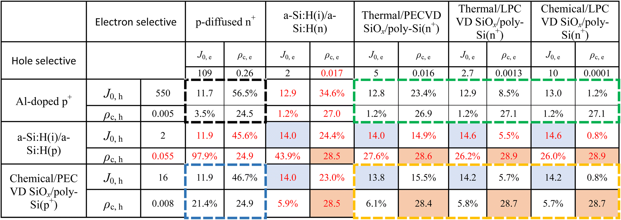
Solar energy is a renewable energy source and the most representative green energy source, because of its non-toxic, harmless, non-polluting, inexhaustible characteristics.1 Silicon is an indirect bandgap semiconductor with a band gap of 1.12 eV, corresponding to a cut-off wavelength of light absorption wavelength of about 1160 nm, and its bandgap closely matches the solar spectrum and photogenerated electrons/holes can exhibit a long lifetime.2 At present, crystalline silicon (c-Si) cells occupy 95% of the global market share and are currently the most important photovoltaic technology.3,4 With a newly installed capacity of over 100 MW per day on average, photovoltaic (PV) solar cells have become the fastest growing class of solar energy–harvesting technologies.5 The large-scale deployment of PV has been mainly based on diffused junction silicon solar cells. The increased quality of c-Si wafers at acceptable cost, dielectric surface passivation schemes, and the possibility of making direct metal–silicon contacts on relatively lightly doped surfaces have been important factors.6,7 The device physics underlying such solar cells is well understood, and the theory coupled with device and material characterization has been an important contributing factor to the increasing sophistication of solar energy technologies. SHJ solar cells have attracted a lot of attention in the past few years due to its high performance, reasonable production cost.8 In SHJ solar cells, an intrinsic hydrogenated amorphous silicon (a-Si:H) layer provides passivation of the Si wafer, a doped hydrogenated amorphous silicon (a-Si:H) layer provides good vertical conductivity and a suitable work function for carrier selection, and a well-designed transparent conductive oxide (TCO) reduces sensitivity to the work function of the metallic terminals, in addition to providing lateral current transport and light coupling. According to theoretical calculations, the limiting efficiency of SHJ solar cells reaches 29.4%.9 Analyses on series resistivity (Rs) explicit that the upper bound for the sum of contact resistivities for p-type (ρc,p) and n-type (ρc,n) contacts is 0.073 Ω cm2.10 With the continuous improvement of contact resistivity, it comes to the conclusion that the theoretical limiting efficiency estimated by Brendel's formulation is 28.5% for SHJ solar cells which is shown in Table 1.11 The limiting efficiency of PERC inhibits further development, but SHJ and Tunnel Oxide Passivated Contact (TOPCon) solar cells are the next direction of industrial renewal and research. In the case that the limit efficiency difference between TOPCon and SHJ solar cells is minor, low temperature production and simple production line process have become the main advantages for SHJ.13| a Box with blue background: combined selectivity greater than 14. Box with pink background: combined selectivity greater than 28%. Red dotted line: SHJ solar cell. Black dotted line: PERC solar cell. Blue dotted line: p-type TOPcon solar cell. Green dotted line: n-type TOPcon solar cell. Orange dotted line: Bi-facial TOPcon solar cell. |
|---|
|
Due to the advancements in silicon ingot growth processes, defect engineering, and contamination control during solar cell manufacturing, the bulk electronic quality of c-Si wafers has been enhanced to a degree where further device improvements now depend on innovative interface passivation and carrier-selective contact structures. A high-quality passivation layer is a key requirement to optimize the performance of SHJ solar cells.14 The improvement of SHJ solar cells efficiency now mainly relies on innovative interface passivation and carrier selective contact structures, which become the focus of current research. Currently, high-quality a-Si:H deposited by radio-frequency plasma enhanced chemical vapor deposition (RF-PECVD) is widely used for passivation of c-Si surfaces, which can reduce the recombination loss of the silicon surface and obtain higher open-circuit voltage (VOC).15 This review focuses on the conditions for depositing a-Si and corresponding improvements to the carrier selection layer, such as nanocrystalline silicon (nc-Si), or nc-Si alloy with oxygen (O) and carbon (C). Novel transparent electrodes for SHJ have been explored to further reduce improve optical and electrical properties (high transmittance and low resistance) as well as production costs (less or no use of In). Finally, the tandem solar cell with SHJ solar cells is introduced, which would exhibit more than 35% of high-efficiency solar cells. Further research is focus on the various compositions of SHJ solar cells, thus ensuring that the efficiency of SHJ solar cells continues to improve.
2. Theories and measurements of SHJ solar cells
High-efficiency silicon-based solar cells are mainly improved through heterojunction structure with a-Si:H thin films as the passivation layer. Fig. 1a shows the schematic diagram of a traditional bifacial SHJ solar cell structure and Fig. 1b is the corresponding schematic band structure diagram. Fig. 1c gives the schematic diagram of an SHJ-IBC solar cell structure, and Fig. 1d presents the typical TOPCon solar cell structure with ultrathin SiOx as a passivation layer. TOPCon and SHJ solar cells are two important directions for industrialization. At present, among silicon solar cells technologies, aluminum back surface field (Al-BSF) solar cells and passivated emitter and rear cells (PERC) dominate the production of large-scale industrial PV devices.16 In Al-BSF and PERC solar cells, photogenerated minority carriers are collected by emitters formed by a dopant diffusion process. The main difference between the two structures is on the rear side, where the full area aluminized back contact is replaced by a dielectric passivation layer (such as an alumina layer) and a local aluminized contact. This evolution reduces the recombination current density on the rear side. However, due to the use of silicon–metal contacts on the front and back, severe recombination current densities can result in VOC loss.17,18 | ||
| Fig. 1 (a) The structure of SHJ solar cell; (b) energy band diagram of SHJ solar cell; (c) the structure of IBC-SHJ solar cell and (d) the structure of TOPCon solar cell. | ||
Passivation contact technology can significantly reduce the contact recombination loss, and the two representative technologies are TOPcon and SHJ.19 TOPcon solar cell follows the PERC technology, by using SiOx/poly-Si passivation contact to replace the original metal contact (mainly the back) structure to provide an excellent surface passivation for the back of the silicon wafer, and thus improve the open circuit voltage as well as short circuit current.20 The high performance of SHJ solar cells comes from surface passivation with thin intrinsic a-Si:H layers on the front and back, and the results show that with this structure, more than 750 mV of VOC and more than 85% of FF can be obtained.21 TOPCon is based on the PERC process (high temperature process), adding the preparation of tunnel oxide layer and polysilicon layer, and the production line is simple to upgrade. However, PERC and TOPCon exhibit scalability limitations because they rely on silver contact formation. This is especially evident in TOPCon solar cells, where the extensively used laser-enhanced contact optimization (LECO) process is applicable only to fired silver contacts.22
For solar cells, generally think of the ideal solar cell to calculate, that is, the series resistance is zero, and the parallel resistance is infinite. When the solar cell is in an open circuit state, I = 0, R = ∞. The expression for VOC is as follows:
 | (1) |
When the solar cell is exposed to light, the external circuit is short-circuited. At this time, the short-circuit current (JSC) is equal to the Iph, which is proportional to the incident light intensity, and the JSC can be expressed as the following equation:
| ISC = I = Iph | (2) |
The fill factor (FF) is defined as the ratio of the maximum power output of the solar cell to the product of short-circuit current and open-circuit voltage:
 | (3) |
The percentage of the maximum power absorbed by the solar cells connection to the total radiant power incident on the cell is defined as the power conversion efficiency (PCE) of the solar cells η:
 | (4) |
The implied-VOC (iVOC) of solar cells can be obtained through minority carriers' lifetime.23 There is no external current in the open-circuit solar cell, and the photogenerated current is balanced with the recombination current (Jph = Jrec). In solar cells with thickness W, the photogenerated current density Jph has the following relationship with the effective carrier lifetime τeff:
 | (5) |
One of the major factors on the performance of SHJ are J0 and ρc, in the design of solar cells to reduce the cell J0 and ρc can significantly improve the performance of SHJ, lower J0 and ρc are beneficial to improve the selective carrier transportation. Eqn (1) shows that VOC is controlled by J0, and thus lower J0 leads to higher VOC. J0 is related to the intrinsic carrier concentration in the material, and changes dramatically with the change of temperature, J0 has a great influence on VOC, obviously.25
Reverse saturation current (J0) consists of two main components, namely reverse saturation diffusion current J01 and reverse saturation compound current J02. Recombination currents include in bulk recombination currents, surface recombination currents (J0S) and space charge region recombination currents (J0scr). For semiconductor materials, intrinsic recombination (radiation recombination and auger recombination) is a property of the material itself, which can only be eliminated by improving the quality of the material. The internal trap recombination can be reduced by improving the quality of the material. The magnitude of the recombination current in the bulk is mainly determined by the lifetime of the minority carriers, which satisfies the following relation:
 | (6) |
For the surface recombination current, it can be expressed by the following formula:24
 | (7) |
 | (8) |
 | (9) |
 and
and  are the electron and hole diffusion lengths, respectively. For metal–semiconductor contact:
 | (10) |
 . Φn is the actual barrier height formed by metal–semiconductor contact. Charge carriers should be transferred and extracted as much as possible to reduce the current loss caused by recombination, which can improve the photocurrent and reduce the dark saturation current, thereby improving the VOC of the solar cells.
Both J0 and ρc have great impact on carrier selectivity. ρc is determined by the following relation:
 | (11) |
The selectivity of minority carriers is determined by the formula:25
 | (12) |
For practical purposes, it is worth noting that among all available techniques for measuring ρc, the most straightforward are the transfer length method (TLM) and circular transmission line method (CSM). Similarly, research groups reported that in SHJ solar cells, high efficiency depends not only on outstanding passivation but also on low ρc. Fig. 2a displays the typical TLM structure used for characterizing c-Si solar cells, in the conventional TLM model, guaranteeing the ohmic contact between the electrode and the Si substrate is necessary to extract ρc. The total resistance (RT) can be expressed as the following:26
 | (13) |
 | (14) |
 | (15) |
 , hence ρc = RCWL; in contrast, when W ≤ 0.5WT, in this case, RC can be approximated as:
  , hence ρc = RCLWT.
 | ||
| Fig. 2 (a) Typical TLM structure used for characterizing c-Si solar cells. The total resistance RT is obtained by calculating the J–V data between the electrodes at different distances d, by application of a dc voltage V and measurement of the current (c) fitted curve of total resistance versus contact spacing (reproduced from ref. 26 with permission from Elsevier, copyright 2017). (b) Configuration of the conventional Cox–Strack measurement. The total resistance RT is measured from a top contact of diameter d through a semiconducting substrate of thickness t to a back contact by applying a DC voltage V and taking the measurement of the current. (d) Plots of RT–RSversus d−2 and the corresponding linear fitting curve, and the slope of the curve is the specific contact resistance ρc (reproduced from ref. 27 with permission from Elsevier, copyright 2022). | ||
The CSM model was first proposed by Cox and Strack in 1967, Fig. 2b and c show the general structure of CSM measurement and the plot of RT–RSversus d−2, respectively. Theoretically, the total resistance (RT) in a circuit can be expressed as:27
| RT = RC + RS + R0 | (16) |
 | (17) |
 | (18) |
The direction of the charge carriers and charge current density in the test structure should match the direction of the photocarriers in the solar cell. The main reason is that the direction of the charge carriers in the test structure doesn't match the direction of the photo-induced carriers in the solar cell, using the TLM method to test contact resistance is likely to introduce a large error in the data.
3. Historical development of SHJ solar cells
In the late 60s of the 20th century, the discovery of hydrogenated amorphous silicon (a-Si:H) led to the development of electronic properties of a-Si:H with reasonable carrier mobility.29 The first solar cell using the SHJ structure consisted of the bottom cell of the a-Si:H/polysilicon heterojunction in a tandem solar cell, which was patented in 1985.30 In 1991, Sanyo Corporation obtained a hybrid design patent for SHJ solar cells under the trademark HIT (Heterogeneous Intrinsic Thin Layer), which increased the efficiency of HIT cells by 18.1%. With the further upgrading of the process, the efficiency of SHJ was over 20% in 2000,31 as shown in Fig. 3a. And then by reducing the carrier concentration of transparent conductive oxide (TCO) films to reduce free carrier absorption (FCA) and increasing Hall mobility to optimize transverse conductivity, Sanyo improved the efficiency of SHJ to 24.7% in 2014.39 In 2014, Panasonic combined HIT technology with the IBC concept to achieve an efficiency of 25.6%.40 In 2017, Kaneka Corporation achieved a record efficiency of 26.63% with their single-junction SHJ-IBC devices, and this technology combines the interdigital back contact (IBC) structure with SHJ solar cells to significantly reduce parasitic absorption from a-Si:H and TCO layers, resulting in improved power conversion efficiency,32 as shown in Fig. 3b. Concurrently with the advancement of n-type silicon, there has been a parallel improvement in the comprehension of LID in p-type silicon. It was not until the mid-to-late 90s of the 20th century that degradation mechanisms involving boron pairs (introduced as dopant atoms) and oxygen pairs (introduced in large concentrations by the Cz process during crystal growth) were discovered.41 In 2015, the efficiency of double-sided batteries has also been greatly improved, and a large-size (151.9 cm2) solar cell with a conversion efficiency of 25.1% has been achieved, see in Fig. 3c.33 In February 2018, ISFH prepared an IBC structure solar cell based on p-type silicon, which achieved an efficiency of 26.1%,34 and the current champion efficiency of SHJ solar cells of p-type silicon is 26.56% created by LONGi in October 2022.42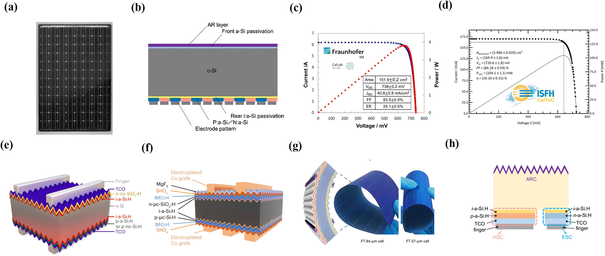 | ||
Fig. 3 (a) The world's first industrialization of a-Si/c-Si hybrid solar cell produced by Sanyo and an efficiency of 15.2% was gained (reproduced from ref. 31 with permission from Wiley, copyright 2000). (b) Cross-sectional schematic drawing of the HJ-IBC solar cell, which reached a record 26.7% in 2017 (reproduced from ref. 32 with permission from Elsevier, copyright 2017). (c) The first both-side-contacted c-Si solar cell to break through 25.1% efficiency in 2015 (reproduced from ref. 33 with permission from American Institute of Physics, copyright 2015). (d) Light J–V curve and power in dependence of the voltage of the POLO-IBC cell measured at the ISO 17025-accredited Calibration and Test Center, ISFH-CalTeC. The power conversion efficiency of the POLO-IBC cell is 26.10% (reproduced from ref. 34 with permission from Elsevier, copyright 2018). (e) Device structure of LONGi SHJ solar cell with p-type doped nanocrystalline silicon and a low sheet resistance transparent conductive oxide, which won the high PCE of 26.81% (reproduced from ref. 35 with permission from Springer Nature, copyright 2023). (f) Device structure of Maxwell prepared SHJ solar cells with plating copper electrode and double-sided indium-based transparent (dopant-free SnOx: IMO![[thin space (1/6-em)]](https://www.rsc.org/images/entities/char_2009.gif) :H = 1:1) electrodes, and a certified efficiency of 25.94% was achieved (reproduced from ref. 36 with permission from Springer Nature, copyright 2023). (g) Ultra-thin (57 μm) flexible SHJ solar cell prepared by LONGi, which exhibited the high power-to-weight ratio (1.9 W g−1) and open-circuit voltage (761 mV) (reproduced from ref. 37 with permission from Springer Nature, copyright 2024). (h) Device structure of heterojunction back contact (HBC) solar cell with an efficiency of up to 27.09% (reproduced from ref. 38 with permission from Springer Nature, copyright 2024). :H = 1:1) electrodes, and a certified efficiency of 25.94% was achieved (reproduced from ref. 36 with permission from Springer Nature, copyright 2023). (g) Ultra-thin (57 μm) flexible SHJ solar cell prepared by LONGi, which exhibited the high power-to-weight ratio (1.9 W g−1) and open-circuit voltage (761 mV) (reproduced from ref. 37 with permission from Springer Nature, copyright 2024). (h) Device structure of heterojunction back contact (HBC) solar cell with an efficiency of up to 27.09% (reproduced from ref. 38 with permission from Springer Nature, copyright 2024). | ||
Subsequently, LONGi successfully introduced the nano-crystallization process into the fabrication of the tip HSC with corresponding TCO. The front finger was fabricated by laser transfer process to reduce the shading ratio from 2.8 to 2.0%, the window layer of the front finger was optimized to reduce parasitic absorption, a MgF2/Ag reflective layer was added on the back side, and the ITO was replaced by ICO. These improvements improved VOC and JSC of SHJ solar cells, and a certified PCE of 26.81% was achieved.35 What's more, LONGi still holds the title for champion efficiency of mono-crystalline silicon heterojunction solar cells, and the solar cell with Heterojunction Back Contact (HBC) structure has a certified efficiency of 27.30%.21 In recent year, Maxwell has made significant advances in copper plating, SHJ solar cells were fabricated using doped nc-SiOx:H as a passivation contact layer, which exhibited excellent electron selectivity, low parasitic absorption, and high uniformity, additionally, seed-free copper plating with high aspect ratio and low metal fraction was employed.36,43 Finally, a certified efficiency of 26.41% is obtained for M6-size bifacial silicon heterojunction devices, as shown in Fig. 3e. Regarding the development of flexible solar cells, Liu et al.44 prepared a flexible solar cell with high efficiency (>24%), a large area (>240 cm2) with edge-blunting passivation technology, in August 2022. This technology enabled to improve the flexibility of silicon wafers by blunting the pyramidal structure in the marginal regions. In 2022, LONGi developed a large-area (274.4 cm2) flexible SHJ solar cell with a minimum thickness of 57 μm, which has a very high power-to-weight ratio of 1.9 W g−1 and a high VOC of 761 mV.44 The development of flexible solar cell technology provides a practical basis for creating lightweight, low-cost, high-efficiency SHJ solar cell devices.
Historically, the main design concepts that have been proven to be critical to improve c-Si technologies, the concepts are as follows: (i) a rear surface field below the rear contact; (ii) effective surface texture for light capture; (iii) surface passivation of c-Si surfaces and (iv) contact structure (conventional structure and BC structure). Table 2 describes the corresponding devices in this article, including solar cells with small-and large-are bifacial contact amorphous silicon or polycrystalline silicon passivation layer from laboratories and enterprises.
| No. | Wafer type | V OC (mV) | J SC (mA cm−2) | FF (%) | E ff (%) | Year | Production agency |
|---|---|---|---|---|---|---|---|
| 1 | n-type | 750 | 39.5 | 83.2 | 24.7 | 2014 | Sanyo39 |
| 2 | n-type | 740 | 41.8 | 82.7 | 25.6 | 2014 | Panasonic40 |
| 3 | n-type | 738 | 40.8 | 83.5 | 25.1 | 2015 | Kaneka corporation33 |
| 4 | n-type | 729 | 40.7 | 76.4 | 22.6 | 2017 | EPFL45 |
| 5 | n-type | 738 | 42.7 | 84.9 | 26.7 | 2017 | Kaneka corporation32 |
| 6 | n-type | 736 | 41.5 | 81.9 | 25.0 | 2020 | CSEM46 |
| 7 | n-type | 730 | 40.3 | 82.3 | 24.2 | 2020 | CSEM46 |
| 8 | p-type | 723 | 40.7 | 80.8 | 23.8 | 2020 | CSEM46 |
| 9 | n-type | 747 | 39.6 | 84.9 | 25.1 | 2020 | Hanergy47 |
| 10 | n-type | 725 | 40.9 | 80.9 | 24.0 | 2021 | Jülich48 |
| 11 | n-type | 751.4 | 41.45 | 86.1 | 26.81 | 2023 | LONGi35 |
| 12 | p-type | 751.3 | 41.29 | 85.59 | 26.56 | 2024 | LONGi42 |
| 13 | n-type | 750.2 | 40.79 | 86.28 | 26.41 | 2023 | Maxwell43 |
| 14 | n-type | 761.3 | 40.22 | 85.13 | 26.06 | 2024 | LONGi37 |
| 15 | n-type | 742.5 | 42.61 | 85.60 | 27.09 | 2024 | LONGi38 |
| 16 | n-type | 743.4 | 42.62 | 86.19 | 27.30 | 2024 | LONGi21 |
4. Passivation contact materials and device applications in SHJ solar cells
For a solar cell to function, there must be a selective transport of charge carriers. The theoretical method to achieve carrier selectivity is to directly add conductive layers to c-Si silicon wafers with asymmetric work functions (ϕ) at the conduction and valence band edges. In this theoretical approach, Schottky–Mott theory is followed, the PCE of solar cells would increase stably with the charge-carriers transportation is fulfilled. In practice, the existence of surface phenomena such as dangling bonds, metal induced gap states (MIGS) and inter-face dipoles, makes it difficult for theoretical methods to be explained using Schottky–Mott theory, resulting in the Fermi level pinning (FLP) which forms a Schottky barrier on the interface.14 To solve this problem passivation contact processes have been developed and SHJ was developed based on this technology. Under the condition of no passivation contact, the metal electrode in contact with Si directly, which makes the carrier recombination extremely, resulting in a high J0, a high contact resistance and a low VOC even leading to the FLP, thus making it difficult to achieve a great breakthrough in the efficiency of solar cells. Passivation contacts are defined as a set of layers that provide both selective conduction of charge carriers and effective passivation of the silicon surface.Passivation quality directly determines the performance of SHJ. The quasi-steady-state photoconductance method (QSSPC) has been widely applied to evaluate the passivation performance of monocrystalline silicon.49,50 Carrier lifetime τeff:
 | (19) |
 | (20) |
It benefits from the excellent properties of passivation contact, the efficiency of silicon solar cells exceeded 25%. Since then, all devices that exceed this mark, whether small or large area, with contacts on either side or back of the silicon wafer, have used at least one passivation contact material. The widespread success of passivation contacts have led to increasing research into ways of forming carrier selective junctions, resulting in a variety of approaches. The schematic representation of the role of passivation contact is shown in Fig. 4. In this review, the passivation contact layer is divided into a passivation layer and a carrier selection layer, and the research and exploration of each layer based on traditional SHJ solar cells are introduced, and promising opportunities towards higher conversion efficiency are emphasized. “Passivating contact”, which may appropriately be called a “passivating junction”,54 encompasses several of the functions necessary for the efficient operation of a solar cell device: passivate surfaces and interfaces, provide a high conductivity for just one type of charge carrier, and establish a bridge between the work functions of silicon and silver (Ag) or aluminum (Al), the metals commonly used to form the electrodes. The passivation contact layer can generally be grown by chemical vapor deposition (CVD), including plasma enhanced chemical vapor deposition (PECVD) and hotwire chemical vapor deposition (HWCVD). Compared with PECVD, the film growth rate of HWCVD is relatively high and the order is better, and HWCVD can efficiently decompose H2 to produce a very high density (>1014 cm−3) of H atoms, which helps to improve the passivation quality. However, HWCVD does not control the substrate temperature accurately enough during the deposition process, which will affect the deposition rate and crystallization rate of the film.55
 | ||
| Fig. 4 Schematic representation of the role of passivation contact as an intermediate layer between light absorber and metal contact, the passivated contact layer forms different resistivity to electrons and holes to enable carrier selection (reproduced from ref. 53 with permission from Elsevier, copyright 2022). | ||
4.1 Passivation layer materials
Excellent surface passivation is the key technology of high-efficiency c-Si cells,56,57 it is necessary for the preparation of high-performance devices. The passivation mechanism of materials is usually divided into field passivation58 and chemical passivation.59 Field effect passivation reduces surface recombination by generating an electrostatic field at the interface through charge accumulation that drives photogenerated carriers away from the surface, such as Si3N4 and Al2O3; chemical passivation refers to through chemical bonds in materials with silicon surface suspension bonding, thus reducing the silicon surface suspension density and reducing deficiency trapping, reducing the recombination of photogenerated carriers, such as H in a-Si:H. The role of the passivation layer film in heterojunction solar cells is extremely important. At present, the passivation layers of crystalline silicon, mostly are a-Si:H and SiOx materials.Substrate temperature is critical to improve solar cell performance. Fig. 5 shows the effect of substrate temperature on deposited amorphous silicon layers, which can be obtained that the a-Si band gap decreases with the increase of temperature. When the substrate temperature is about 210 °C, the lifetime is the highest, and the FF of the device is also the highest.63
 | ||
| Fig. 5 (a) Double-sided SHJ structure (b) substrate temperature and a-Si:H function relationship, as the temperature increased, the a-Si band gap decreased from 1.84 to 1.80 (c) effect of temperature on a-Si:H minority carrier lifetime, optimal passivation results and high minority carrier lifetime are achieved at around 210 °C (d) influence of substrate temperature on J–V curve, prove the optimal passivation effect at about 210 °C (reproduced from ref. 63 with permission from Springer, copyright 2019). | ||
In the PECVD system, different effects of intrinsic passivation layers are also deposited through different frequencies. Compared to the frequency of 40.68 MHZ, Hanergy Group use 13.56 MHZ through the RF-PECVD system, and the deposited film can achieve an efficiency advantage of 0.21%, and on a total area of 244.5 cm2, obtain ISFH certified 25.11% efficiency.47Fig. 6 shows cross-sectional TEM images of deposition at different frequencies, respectively. VHF-PECVD-prepared a-Si produces more severe epitaxial growth, resulting in more light absorption. Low deposition rates produce non-dense thin films that prevent epitaxial growth of c-Si and improve passivation. Therefore, the deposition frequency must be controlled to obtain better performance when the amorphous silicon is deposited under different conditions.
 | ||
| Fig. 6 Cross-sectional TEM images taken at the a-Si:H/c-Si interfaces with (a) RF-PECVD and (b) VHF-PECVD deposited i-a-Si:H layers. (a) TEM images deposited using RF (13.56 MHz) (b) TEM images deposited using VHF (40.68 MHz), thin films deposited at different frequencies have different deposition rates, and high deposition rates in VHF-PECVD can prevent epitaxial growth (reproduced from ref. 47 with permission from Elsevier, copyright 2020). | ||
Under conditions of high pressure and high power, very thin, loose a-Si:H films with high structural factors deposited in pure silane plasma always form a mutant interface, and after the deposition of the p-a-Si:H layer, passivation will produce some degradation. National Institute of Advanced Industrial Science and Technology (AIST) utilizes an extremely thin low-density intermediate layer and a dense overlay, which ultimately leads to the preparation of high performance SHJ with a passivated a-Si/c-Si interface.64 A double-layer passivation structure is formed through the buffer layer deposited by pure silane plasma, which effectively reduces the risk of epitaxial growth of thin films and plasma damage caused by hydrogen-diluted silane plasma.65 On an area of 238.95 cm2, a PCE = 22.43% was achieved. Solar Energy Technology Laboratory (STL) in Thailand has shown higher efficiency by replacing the a-SiO:H(i)/a-Si:H(i) tandem passivation layer with an a-SiO:H(i) tandem passivation layer, and the efficiency obtained was 19.4%. These experimental results show that the alloying and stacking of intrinsic layers can provide an efficient development path for SHJ solar cells by enhancing passivation and tuning photoelectric characteristics. To overcome epitaxial growth and recombination sites, many institutions have carried out changing the single-layer passivation layer to a multi-layer structure to improve the passivation quality.
It was found that for single intrinsic layer, surface passivation property is best just before the transition from amorphous to micro-crystalline,66 presumably because the a-Si:H network is most relaxed in that case and comprises the lowest dangling bond density.67 Therefore, careful control of the a-Si:H deposition parameters is necessary. Compared with monolayer structures, multilayer structures can reduce the requirements of monolayer film deposition through a series of treatments, i.e., the combination of efficient hydrogenation and the avoidance of epitaxial growth.65 A void-rich a-Si:H interfacial layer (i1) deposited in pure SiH4 plasma in combination with a dense a-Si:H layer (i2) deposited in highly H2 diluted plasma has been shown to increase the passivation quality of SHJ cells (compared to single intrinsic layers deposited in the transition zone between amorphous and micro-crystalline Si).68 Multilayer structures are also considered to achieve good passivation. Fraunhofer Institute for Solar Energy Systems studied the excellent improvement of two-layer intrinsic amorphous silicon for n-type contact and p-type contact by changing the deposition parameters for the i1 layer and i2 layer respectively, as shown in Fig. 7, confirmed that the addition of dense i2 layer does not affect the contact resistance (ρc), and the use of porous i1 layer and hydrogen plasma treatment (i1 + HPT) significantly improved iVOC. The i1 + HPT + i2 stacks (where i1 and i2 are both 3 nm thick) show the best passivation, but ρc is also the highest. i1 Layer is necessary for good passivation of holes and electronic contacts, but it is also primarily responsible for resistance loss.69
 | ||
| Fig. 7 Effect of multilayer structure on (a) n-type and (b) p-type contacts comprising different undoped a-Si:H layer (stacks) as indicated, different colors represent different cumulative post-deposition thermal treatments of 10 min each. At different temperatures, the VOC of the double-layer intrinsic layer structure is increased by more than 20 mV compared with the single-layer intrinsic layer or the non-intrinsic layer structure on the n-type substrate and p-type substrate (reproduced from ref. 69 with permission from Elsevier, copyright 2022). | ||
Though i-a-Si:H has excellent passivation effect, there are also some unsolved problems. Such as a-Si:H layer is greatly affected by temperature and began to deteriorate above 300 °C, and the passivation layer will produce hydrogen overflow at high temperature, so that the suspension bond cannot be passivated. The temperature in the production line must be precisely controlled to prevent hydrogen spillage at temperatures ranging from 200 to 300 °C. Unlike most other silicon solar cell structures, SHJ involves doped heat diffusion to form junctions. The implication is that any subsequent process step following the formation of a-Si:H passivation contacts must operate at temperatures below 300 °C. Consequently, fire protection through metallization becomes necessary, which entails the use of specialized and more expensive low-temperature metallic silver paste. Due to the low transverse conductivity of the a-Si:H layer, a transparent conductive electrode (TCO) is required at the top of the a-Si:H stack for transverse carrier transport, work function alignment, and anti-reflection. TCO and a-Si:H stacks produce some parasitic light absorption over a short wavelength range. This results in a 1–2 mA cm−2 reduction in JSC compared to traditional doped diffusion junctions, which reduces device efficiency. In addition, the presence of non-negligible vertical contact resistivity through the a-Si:H stack also has an impact on device efficiency.70
In the laboratory, PECVD is commonly used for the deposition of amorphous silicon films. In the preparation of SiOx in PRCVD, we typically tune the bandgap and conductivity of the material by introducing CO2 into the reaction gas.80 As shown in the Fig. 8a and b, in the absence of CO2 ingress, an epitaxial layer is found between the a-Si:H/c-Si interface, and the interface also exhibits a certain roughness, which impairs the passivation quality. The AIST tunes the material properties by controlling the CO2 ratio, and the observed change of Eg in the range of 1.87 to 2.23 eV,82 which is shown in the Fig. 8c. Absorption in a-SiO:H films decreases due to the gradual increase of Si–O bonds in the membrane. As shown in the Fig. 8d, after the doping concentration is greater than 0.32, τeff decreases rapidly with the increase of CO2 gas flow due to the lack of abundant hydrogen content in the a-SiO:H film. However, when excess oxygen atoms are bonded into the a-SiO:H film, the passivation quality deteriorates, which leads to the formation of silicon dangling bonds in the interface between the c-Si wafers, resulting in ineffective passivation through the film.
 | ||
| Fig. 8 (a) HRTEM image without CO2, a partial epitaxial layer is found between the a-Si:H/c-Si interface, even though the passivation layer provided abundant hydrogen content (b) with CO2/[CO2]/[SiH4] = 0.32, the partially epitaxial phase was suppressed and an abrupt interface was formed with excellent surface passivation by terminating the dangling bonds (c) curve of band gap with CO2 concentration (d) the results of τeff and the upper limit of Seff for various ratios of [CO2]/[SiH4], the τeff increased and reaches the maximum value of 860 μs (Seff = 17.4 cm−1 s−1) for increasing the ratio of [CO2]/[SiH4] from 0 to 0.32. After the maximum values, τeff rapidly decreased with an increasing CO2 gas flow rate due to the lack of abundant hydrogen content in the a-SiO:H films (reproduced from ref. 81 with permission from Elsevier, copyright 2015). | ||
The PECVD-grown a-Si:H and a-SiOx:H thin films are usually used as passivation layers in the SHJ solar cells. The extremely thin intrinsic i:a-SiOx:H doped with oxygen is beneficial for the inhibition of epitaxial growth, but it is associated with a reduction in the electrical properties of the passivation contact. Based on an earlier HJT efficiency record of 25.11% (an ultra-thin 0.5 to 1.0 nm buffer layer rich in H content was utilized to improve passivation), LONGi introduced O-terminated Si surfaces grown by a self-limiting wet chemical oxidation process (using a HF/H2O2 solution) to inhibit Si epitaxial growth. Subsequently, 2–3 atomic layers of oxidized amorphous silicon subnanometer layer (<0.5 nm; i:a-SiOx:H(1) x ≈ 10 at%) are formed. The ultra-thin i:a-SiOx:H(1) passivation layer prevents the periodic outward extension of the c-Si crystal arrangement, while minimizing the effect of oxygen doping on the electrical properties of the passivation contacts. In the second step, two increasingly dense a-Si:H(i) layers are deposited on i:a-SiOx:H(1), as shown in Fig. 9a. The treatment of these layers minimizes the epitaxial growth region, which leads to more defective interfaces and provides the hydrogenation of the interface. Correspondingly, it reduces defect activity and enable efficient carrier transport. LONGi demonstrates a sandwiched passivation layer (i0/i1/i2) with an H-rich porous first layer (i0) deposited on oxygen-modified c-Si surface, see in Fig. 9c.21
 | ||
| Fig. 9 (a) Structure schematics of the flexible SHJ solar cells with a two-stage composite gradient passivation process (reproduced from ref. 37 with permission from Springer Nature, copyright 2024). (b) Device structure of the solar cell with an efficiency of 26.81%. (c and d) Schematic representation of the front and rear surface fields (reproduced from ref. 83 with permission from Springer Nature, copyright 2023). (e) Three approaches for epitaxy growth suppression, which is a sandwiched passivation layer (i0/i1/i2), with an H-rich porous first layer (i0), deposited on oxygen-modified c-Si surface (reproduced from ref. 21 with permission from Springer Nature, copyright 2024). | ||
4.2 Carriers selective layer materials
In conventional SHJ cells, although the doped a-Si:H window layer is only a few nanometers thick (5–10 nm), it still parasitically absorbs a large amount of incident light, which results in a 1.6 mA cm−2 reduction in the JSC of the solar cell.84,85 In addition, the a-Si:H stack (n ∼ 4.0) increases the reflection of the TCO (632 nm, n ∼ 2.0)/Si (n ∼ 3.8) interface.29 Carrier selection using doped a-Si has achieved 25% efficiency, and to achieve more efficient carrier selectivity, numerous institutions have conducted many exploration experiments on carrier selection layers. To reduce parasitic absorption and reflection, hydrogenated nanocrystalline silicon oxide (nc-SiOx:H) has proven to be a very promising alternative to commonly used doped a-Si:H.86–91 At the same time, the alloying of different elements to produce wider bandgap materials is also a promising development.85,92,93 It is similar to the intrinsic layer, the doped layer can also be stacked to achieve better material properties.Depending on the polarity of the carriers to be collected, the passivation contact is classified into electron-selective and hole-selective contacts, where the carrier transport layer (CTL) is also referred to as the electron transport layer (ETL) and hole transport layer (HTL), respectively. When contacting ETL or HTL with c-Si, the energy band alignment at the c-Si/CTL interface is key to understanding carrier transport mechanisms.
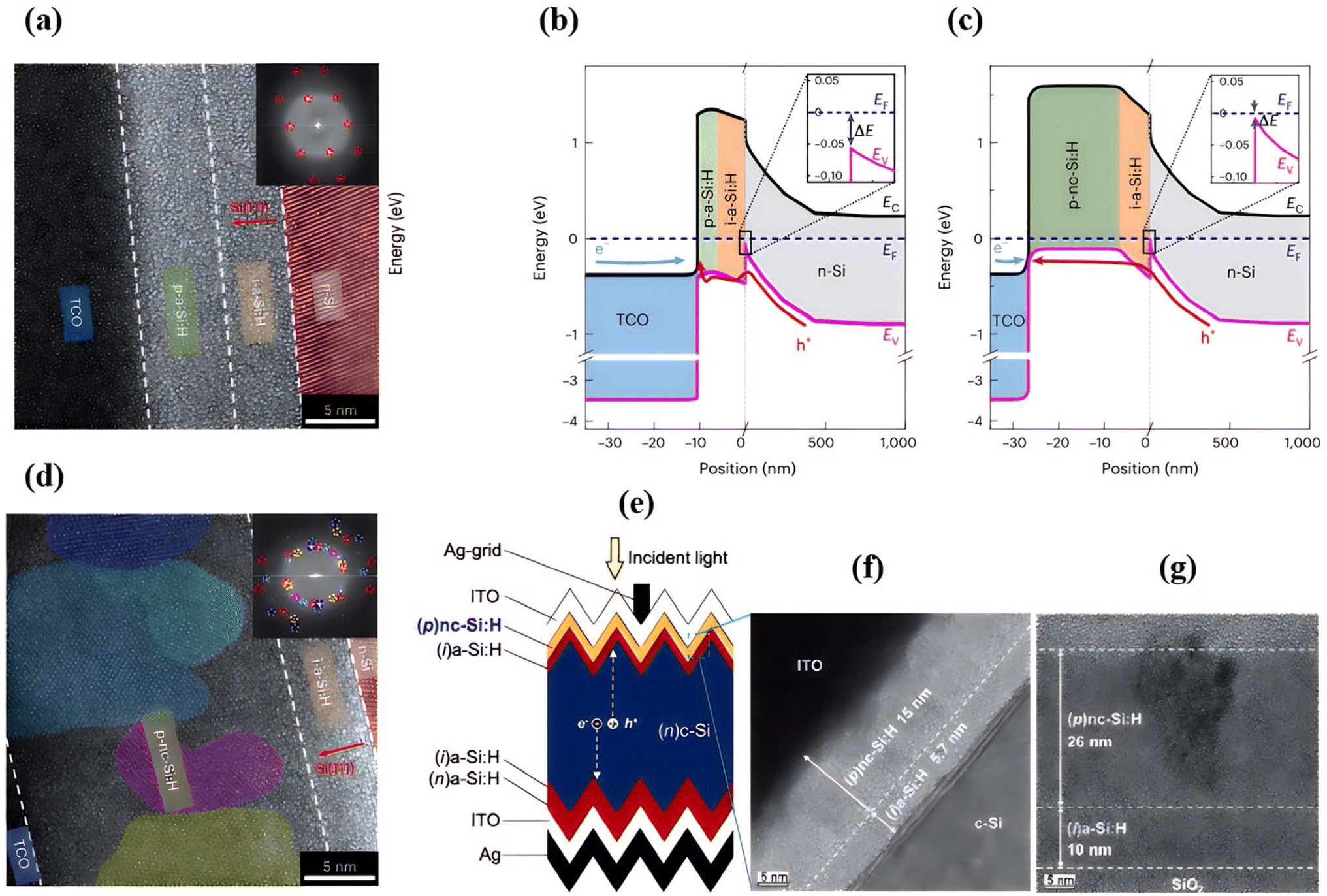 | ||
| Fig. 10 (a and d) TEM images of TCO–p-a-Si:H–i-a-Si:H–n-S (a) and TCO–p-nc-Si:H–i-a-Si:H–n-Si. (b) structures. (b and c) Equilibriumband diagrams of HSCs based on p-a-Si:H (b) and p-nc-Si:H (c) related to the cross-sectional structures in (a) and (d) (reproduced from ref. 35 with permission from Springer Nature, copyright 2023). (e) Schematic diagram of solar cell structure (f) TEM image of textured and (g) flat surface representation under the same deposition conditions, it is seen that the thicknesses of these layers are thinner for textured Si than for planar substrate due to the larger surface area of the textured Si (reproduced from ref. 98 with permission from Wiley, copyright 2020). | ||
Work function is one of the main factors affecting performance, and the work function of the doped a-Si:H layer can be changed by increasing its doping concentration or otherwise replaced by the doped hydrogenated polysilicon layer.99 Many research institutions have conducted a lot of researches on nanocrystalline silicon, and obtained nanocrystalline silicon with different properties by regulating one or more parameters of PECVD.100 By controlling the hydrogen dilution ratio and the ratio of B2H6 to SiH4, the optical band gap, crystallinity and conductivity of the film can be adjusted, and it is observed that nc-Si shows a strong dependence on the conductivity and crystallinity fraction of the film thickness. Due to enhanced field effect passivation (AFP), the effective lifetime of the sample also increases after doping on nc-Si:H. Silicon is an indirect bandgap semiconductor with a low band gap, but silicon nanocrystals change with nc-Si:H size due to the quantum confinement effect,101 so amorphous silicon layers with different bandgaps can be generated to achieve better photoelectric performance.46,47 The nc-Si:H is considered as a more advantageous alternative to the a-Si:H emitter and BSF layers due to nc-Si:H's higher electrical conductivity giving rise to lower series resistance. The conductivity of the doped microcrystalline silicon layer depends largely on the degree of crystallization and the concentration of effective doping, and as the doped gas flow increases, the crystallization will be suppressed, so we must compromise the doping efficiency and the degree of crystallization. Matsumura et al.102 presented that the properties of as-grown silicon films and wafers could be tuned using catalytic doping (Cat-doping) process even after depositions. This Cat-doping process is a post-doping process where dopant gases can be decomposed by catalytic cracking reaction at the hot surface of the wires and, subsequently, the decomposed species contribute to the doping of the silicon surface at a shallow depth. Consequently, the conductivity of Si films can be further improved using this technique.103
As shown in the Fig. 10e–g,98 the AIST designed nc-Si:H(p) for different processes, and Fig. 10b and c shows the cross-sectional TEM image of the stacked nc-Si:H(p)/a-Si:H(i) layers deposited on the textured surface and the planar surface respectively by RF-PECVD under the same deposition conditions. Due to the difference in parasitic absorption loss, the JSC decrease of nc-Si:H(p) is much lower than that of (p)a-Si:H with the increase of the hole contact layer. Although nanocrystals have good characteristics, they need to be applied in well-designed solar cell structures to highlight the advantages of nc-Si:H(p). The deposition rate of nc-Si:H(p) (Rd < 0.02 nm s−1) is lower than that of a-Si:H(p) (≈0.14 nm s−1), and it also plays a role in increasing atomic hydrogen, promoting passivation. Another beneficial effect of using the nc-Si:H(p) contact is to reduce the contact resistivity at the interface, resulting in FF improvement.104 Nevertheless, the TCO layer covering the front and rear of the SHJ solar cell needs to be optimized to balance optical transparency, conductivity, and material cost.54 When IWO replaced ITO, efficiency was further improved.
To increase the optical bandgap and reduce blue light loss, SHJ solar cells, the optical band gap can be widened by the introduction of oxygen.104,105 When the nc-SiOx:H(n) deposition time increases, atomic hydrogen accelerates the nucleation and growth of silicon micro-grains106 and voids may form in the amorphous silicon network near the n-c-Si surface due to the weak bonds are corroded by the active atomic hydrogen. When the deposition time of nc-SiOx:H(n) increases, the conductance monotonically increases, which is due to the increase in the crystallinity of the sample. Between the microcrystalline silicon grains in the layer, the amorphous component is reduced, and the carrier transport between the microcrystalline grains is improved.107 Doped nc-SiOx:H has excellent optical and electrical properties and is one of the most promising materials for SHJ solar cells. Currently, LONGi and Suzhou Maxwell use nc-SiOx:H as the front surface field for SHJ solar cells, and their short circuit currents both exceed 40.50 mA cm−2 and reach up to 41.45 mA cm−1.35,37,43
The nc-SiOx:H(n) increases light transmission but decreases crystallinity. Sichuan University improved the crystallinity of the nc-SiOx:H(n) layer by controlling the high-phosphorus-doped seed crystal layer to form a nucleation layer.107 It can be observed that the light transmission increases after the formation of silicon-oxygen alloy, and then through appropriate PH3 treatment, the crystallization is enhanced and the electrical properties are improved. The nc-SiOx:H(n), evolved from the amorphous phase, grows in columns, and has different orientation, and the introduction of oxygen breaks the Si–Si bonds, making it difficult to grow individual crystals.108 From Fig. 11, when the thickness of the nc-SiOx(n) layer reached to 30 nm, a significant increase in τeff and iVOC was observed, and the J0 value was about 1.68 × 10⁻¹⁴ A cm−2, indicating the breaking of the silicon–hydrogen bond, the diffusion of hydrogen in the C–Si substrate, and the diffusion of phosphorus through the silica layer in the n-type substrate, the passivation quality is enhanced by the addition of the tunnel oxide layer. At an annealing temperature of about 950 °C, the passivation of the field effect due to carrier selectivity decreases and the chemical passivation of ultrafine SiO2 is improved.
 | ||
| Fig. 11 (a) nc-SiOx doped layer structure and (b) contrast structure (c) iVOC and minority carrier lifetimes of samples with three different nc-SiOx(n) layer thicknesses after post-deposition annealing (PDA) measured at an injection level of 1 × 1015 cm−3 (d) Minority carrier lifetimes and iVOC for three different nc-SiOx(n) layer thicknesses in as-deposited state measured at an injection level of 1 × 1015cm−3 (e) the recombination current densities for three different nc-SiOx(n) layer thicknesses in as-deposited state (f) rear recombination current densities of nc-SiOx(n)/SiO2/(n)c-Si/SiO2/nc-SiOx(n) symmetric samples with three different nc-SiOx (n) layer thicknesses (reproduced from ref. 108 with permission from Elsevier, copyright 2022). | ||
Solar cell efficiency can also be improved by controlling different concentrations of doped nc-Si:H(p) stacking. Zhou et al.109 studied the effects of single-layer and multi-layer p-type emitters, including boron-doped hydrogenated nanocrystalline silicon (nc-Si:H) and/or boron-doped hydrogenated nanocrystalline silicon oxide (nc-SiOx:H) films, on the device performance of SHJ solar cells. The novel sandwich-like p-type layer consisting of p-nc-Si:H/p-nc-SiOx:H/p+-nc-Si:H triple layers is proved to be the optimal emitter/window layer, which can be contributed to its high crystallinity, high conductivity and wide bandgap, the final device results are shown in Fig. 12b. This demonstrates the advantages of the multilayer structure, and provides us with directions and ideas for the optimization of the carrier selection layer.
 | ||
| Fig. 12 (a) Diagram of a stacked structure device, from left to right are the sandwich-shaped emitter of p-nc-SiOx:H monolayer, p-nc-Si:H/p-nc-SiOx:H bilayer, p-nc-Si:H/p-nc-SiOx:H/p+-nc-Si:H triple layers. (b) Three different results result in the J–V curve, the double-layer mechanism or sandwich structure shows excellent passivation effect compared to the single-layer structure, achieving higher efficiency (reproduced from ref. 109 with permission from Springer, copyright 2021). | ||
The use of multilayer structures instead of single layers can enhance the SHJ passivation quality and thus improve VOC, and multiple layers are usually beneficial to obtain thin layers with sufficient performance.90 At present, continuous research is also being carried out on multilayer structures, and the band gap will also widen after the introduction of amorphous silicon into C.110,111 As can be seen in Fig. 13, the wide bandgap of n-nc-SiC:H ensures high optical clarity, and the double-layer design achieves good passivation and high conductivity, improved the performance to JSC = 40.87 mA cm−2, FF = 80.9%, and η = 23.99 ± 0.29%. Due to the coexistence of high hydrogen concentration at the n-c-Si/SiO2 interface and passivation of strong field effects, the passivation mass of SiO2/n-nc-SiC:H contact reaches iVOC of up to 740 mV.48
 | ||
| Fig. 13 (a) Schematic diagram of a double-layer structure solar cell, using an n-type wafer with a TPCon front side using nc-SiC:H(n)/SiO2 stack. The back side consists of intrinsic and p-type hydrogenated amorphous silicon (a-Si:H(i/p)) and an ITO layer (b) effect of single-layer structure and bilayer structure on iVOC and (c) ρc at different temperatures (reproduced from ref. 48 with permission from Springer Nature, copyright 2021). Stars show the results for double nc-SiC:H(n) layer (thickness of 9 + 25–30 nm) stack, where Tf of the passivation layer is fixed at 1775 °C and Tf for the conductive layer is varied according to the x axis. The vertical error bars represent the standard error for each measurement in the photo-conductance measurement. The grey box marks the area where the contact resistivity could not be evaluated due to non-ohmic behaviour of the measured data in the case of single nc-SiC:H(n) layers. One sample was used for each data point in the iVOC and ρc measurement. Dashed lines are guides to the eye. | ||
Therefore, the passivation contact avoids direct contact between metal and silicon wafer, reduces interface recombination, and ensures the transport of major carriers. The thin-film materials for both the front and rear surface fields must exhibit high dark conductivity, sufficient carrier-selective properties, and sufficiently small contact resistance properties. In addition, higher optical transmittance is required for thin film materials in the front surface field and improved reflection in the rear surface field as a way to increase the efficiency of SHJ solar cells.
 | ||
| Fig. 14 (a) Band arrangement between n-type ETL material and c-Si, where low ΔEC facilitates electron transport and large ΔEV blocks holes. (b) Band arrangement between p-type HTL material and c-Si, where low ΔEV facilitates hole transport and large ΔEC blocks holes. The band alignment between n-type high-WF TMOs and c-Si, when the EC of TMOs is higher than the EV of c-Si, holes will transport through the (c) B2B tunneling mechanism, and anyway, when the EC of TMOs is a little lower than the EV of c-Si then the (d) TAT is dominant (trap-assisted tunneling effect) (reproduced from ref. 112 with permission from Wiley, copyright 2024). (e) Schematic diagram of DASH (dopant-free asymmetric hetero-contacts) solar cell structure with the TiOx/LiF in the front-side and MoOx in the rear-side (reproduced from ref. 113 with permission from American Chemical Society, copyright 2018). (f-(a)) Standard SHJ and (b) MoOx-based cell schema (reproduced from ref. 114 with permission from Elsevier, copyright 2020). | ||
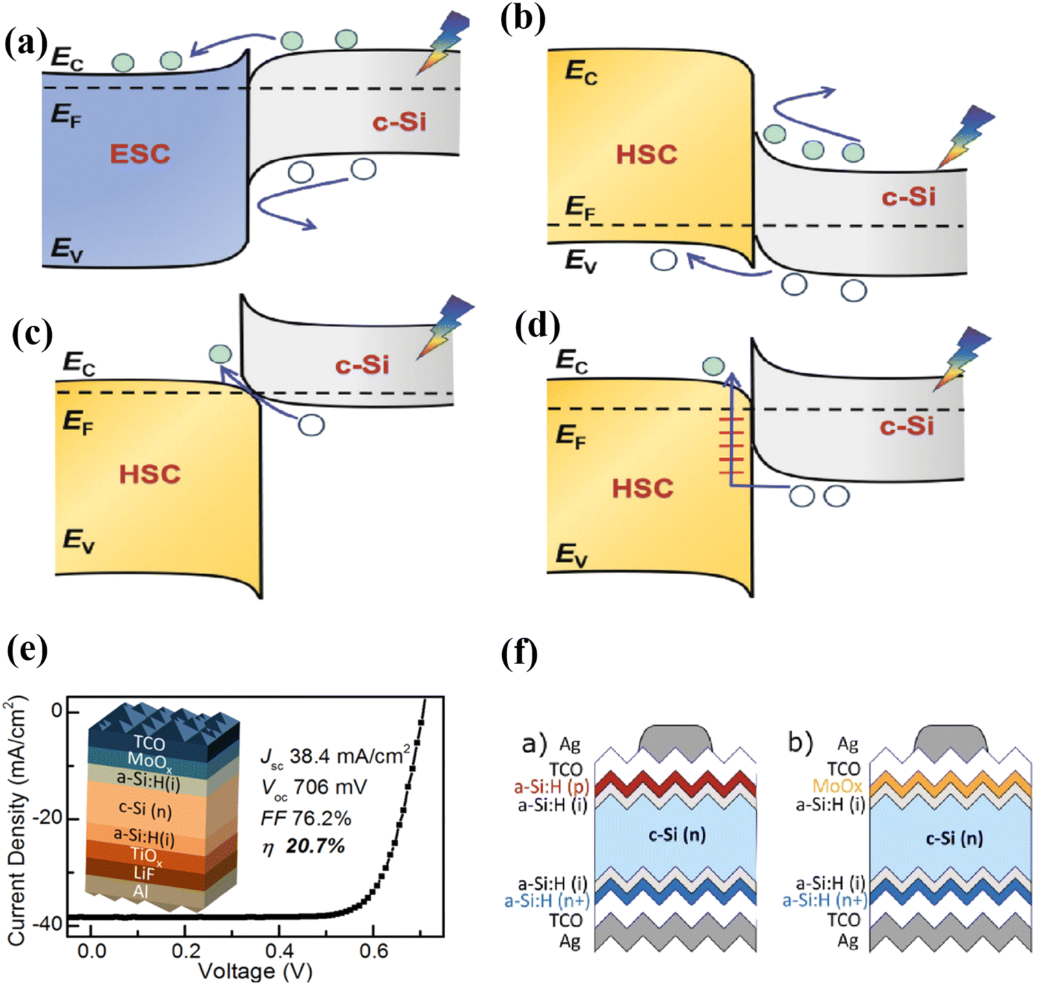
Among the wide-bandgap transition metal oxides (TMOs), for ETL, the energy band arrangement of c-Si/ETL is shown in Fig. 14a. ETL materials are essentially n-type wide-bandgap semiconductors, and they should exhibit a sufficiently small conduction band offset (ΔEC) with respect to c-Si so that electrons in c-Si can be easily transferred to the ETL, while a large valence band offset (ΔEV) is required to block holes, the ETL materials including SnOx,115,116 ZnOx,117 TiOx,118,119 GaOx,120 MgOx,121 NbOx,122 and so on. In 2016, the high-efficiency “dopant-free asymmetric heterojunction” solar cell was reported and achieved a conversion efficiency of 19.7%.123 A second layer of TiOx passivation was added to the LiFx/Al electron-selective contact while maintaining bifacial metallization, resulting in an increased efficiency of 20.7%,113 as shown in Fig. 14e. In addition, the IBC (finger back contact) device structure and MgFx electron-selective contact achieved efficiency of 22.1%.124
For HTLs, there are two main theories, one of which is similar to c-Si/ETL and the other is tunneling effect. The first theory suggests using p-type wide-bandwidth semiconductors as HTL, such as NiO,125 Cu2O.126 The ΔEV at the c-Si/HTL interface is small enough to allow for hole transportation from c-Si to HTL, while electrons are blocked due to the large ΔEC. This approach is theoretically feasible. However, the interface between c-Si and the HTL often has a high density of interfacial defects, resulting in a high contact resistance. Additionally, the concentration of holes in the material is low, leading to poor hole conductivity and insufficient hole selectivity of the contact. Another theory applies to n-type high work function (WF) transition metal oxides (TMOs),127 which can work well as efficient HTLs due to their high WF, such as MnOx (Fig. 14f),118 WOx128,129 and V2Ox,130 which mainly relies on band-to-band (B2B) tunneling effect or trap-assisted tunneling effect (TAT). When the high WF TMOs are in contact with c-Si, the energy band alignment will cause a sharp upward energy band bending on the c-Si surface. The conduction band of these high-WF TMOs is relatively close to the valence band of c-Si, so the photogenerated holes gathered in the valence band of the c-Si absorber can cross the contact interface through the tunneling effect and complex with the electrons in the conduction. The bands of the high-WF TMOs are shown in Fig. 14c and d.
In addition to metal compounds, there are many reports on the carrier transport of other organic materials. Commonly used organic electron transport layers such as poly(ethylene oxide) (PEO),131 branched polyethyleneimine (PEI)132 and C60 pyrrolidine Tris-acid (CPTA)133 have been used in many applications.134,135 Reichel et al.134 promoted the performance of n-type c-Si solar cells with front boron diffusion up to 17.5% when using L-histidine and/or fluorine surfactants as a whole-area back-surface electric field, as shown in Fig. 15a. In addition, He et al.133 improved the performance of n-type c-Si solar cells by independent optimization of hole/electron selective contacts relying only on a solution-based process, with the efficiency of poly(3,4-ethylenedioxythiophene): poly (styrenesulfonate)/n-silicon (PEDOT:PSS/n-Si) HSCs boosting from 12.6% to over 16.7%, as seen in Fig. 15b and c. These materials can effectively improve the contact resistance characteristic of the interface and enhance the carrier selection properties through various mechanisms, but the inherent defects in the surface passivation of these materials lead to the still low efficiency of solar cells. At the same time, most of their preparation methods are solution methods, which are not as simple and fast as the traditional CVD and PVD preparation, resulting in their large-scale applications still have obvious disadvantages.
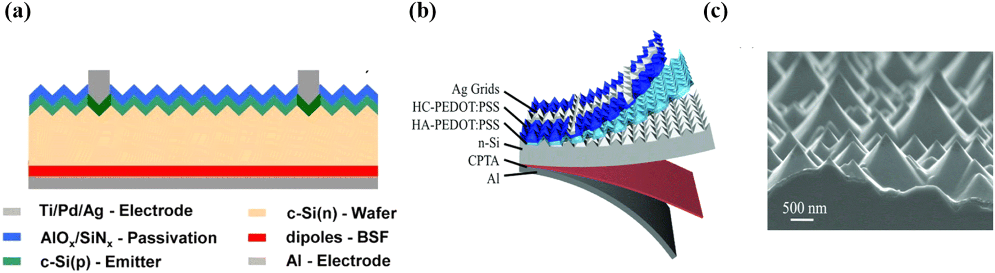 | ||
| Fig. 15 (a) Schematic illustration of the organic silicon heterojunction n-type solar cells with an electron-selective contact on the back, realized by the dipole material and Al as a metal electrode (reproduced from ref. 134 with permission from American Institute of Physics, copyright 2018). (b) Configuration of a PEDOT:PSS/n-Si heterojunction device and (c) SEM image of an HA-PEDOT:PSS film on n-Si pyramids (reproduced from ref. 133 with permission from Wiley, copyright 2018). | ||
Commonly used organic hole transport layers such as poly(3,4-ethylenedioxythiophene) polystyrene sulfonate (PEDOT:PSS)136 have been extensively studied. PEDOT:PSS, should be able to form a conductive passivation material because the PSS species has an excellent passivation effect, being comparable to that of high-temperature annealed SiO2, and PEDOT has a good conductivity, like that of ITO.137–139 By combining PEDOT and Nafion solution to form a composite film, Hebei University experimentally found a coexistence region with good electrical conductivity and passivation and called it PEDOT:Nafion, Nafion film can provide excellent passivation effect, comparable to the best a-Si:H(i) in the photovoltaic field.140 A passivation-conductivity phase plot was made, and selectable conductivity and passivation were achieved by controlling the PEDOT/Nafion ratio. This led to the development of an organic passivation contact cell concept where passivation and hole selectivity occur at the back interface of PEDOT:Nafion/Si organic-inorganic hybrids, eliminating the need for high-temperature processes and complex laser turn-on steps. Commonly used metal compounds and organic materials are summarized in Table 3.
| Material | Carrier polarity | V OC (mV) | J SC (mA cm−2) | FF (%) | E ff (%) | Ref. |
|---|---|---|---|---|---|---|
| SnOx | ETL | 718 | 36.2 | 77.3 | 20.10 | 116 |
| ZnOx | ETL | 672 | 38.23 | 72.0 | 18.46 | 117 |
| TiOx | ETL | 696 | 38.61 | 75.3 | 20.24 | 119 |
| LiF | ETL | 716 | 38.36 | 80.5 | 21.12 | 141 |
| MgOx | ETL | 628 | 39.50 | 80.6 | 20.00 | 121 |
| MgFx | ETL | 718 | 41.5 | 74.2 | 22.10 | 124 |
| NiOx | HTL | 580 | 36.90 | 71.1 | 15.20 | 125 |
| CuOx | HTL | 622 | 38.38 | 82.6 | 19.71 | 126 |
| WOx | HTL | 715 | 31.50 | 81.1 | 17.90 | 129 |
| V2Ox | HTL | 635 | 39.74 | 83.3 | 21.01 | 130 |
| MoOx | HTL | 718 | 41.50 | 74.2 | 22.10 | 124 |
| PEDOT:PSS | HTL | 657 | 38.90 | 80.60 | 20.60 | 136 |
| CNT:Nafion | HTL | 654 | 39.90 | 82.00 | 21.40 | 142 |
| b-PEI | ETL | 641 | 37.60 | 80.70 | 19.50 | 132 |
| CPTA | ETL | 632 | 34.70 | 76.30 | 16.73 | 133 |
| PEO | ETL | 563 | 28.65 | 76.22 | 12.29 | 131 |
5. Other components of SHJ
5.1 Transparent conductive materials (TCMs)
TCM plays a vital role in SHJ solar cells, it is not only the conductive electrode of the solar cell, but also the anti-reflection film of the cell, which can reduce the reflection loss of light and improve the conversion efficiency. The role of TCMs should have the following points: (i) excellent light transmission performance, so that as many photons as possible into the emitter and base region; (ii) control the refractive index to play the role of anti-reflection; (iii) in terms of electricity, achieve the highest possible conductivity.143,144 TCMs are mostly transparent conductive oxides (TCO), and transparent electrodes in optoelectronic devices are often based on indium tin oxide (ITO), which is the most successful TCM used in both academia and industry.145,146 However, owing to the increasing demand and price for the rare material indium (In), alternative transparent electrodes are urgently needed for the development of optoelectronic technology.147–149 To prepare high-quality large area transparent electrodes, it is necessary to use low-cost electrodes produced by low-temperature processes and stable hydrogen (H2) plasma. So, similar to FTO (fluorine-doped tin oxide), although it has a large optical bandgap and stable conductivity in the air environment, it is difficult to use as a transparent conductive material due to the destruction of hydrogen (H2) plasma during the manufacturing process of solar cells and the deposition at high temperatures above 300 °C.150,151Low resistivity, high light transmittance and low temperature growth are the basic requirements for TCO films for SHJ cells.152 The relationship between TCO film resistivity and free carrier concentration and mobility is:
 | (21) |
 | (22) |
High-performance TCO is introduced by optimizing physical properties such as structural geometry and mass density.156,157 Numerical analysis shows that TCO with WF > 5 eV is more suitable for SHJ devices, i.e. allowing the use of thinner and lightly doped a-Si:H films.158 Meanwhile, free carrier absorption (FCA) and hall mobility in TCO have great influence on light transmission. In addition, the high Hall mobility in TCO films means the large wavelength transparency limit, which is characterized by the plasma wavelength λp, here we need to understand the plasma wavelength (λpe), the plasma wavelength (λpe) of the TCO is given by:159
 | (23) |
Fig. 16a shows the requirements for front and rear TCO and possible candidate for TCO application on SHJ solar cells. ITO and doped ZnO can be applied to SHJ solar cells because of high transparency and good conductivity. Research on ZnO is a hot topic, and we will introduce it accordingly below. Fig. 16b shows the results for the sheet resistance and optical transmittance of various types of transparent conductive films that were reported by other research groups.160 The group divided TCMs into four types: doped metal oxides, inorganic metal films, non-oxide, and organic polymer electrolyte films. The sheet resistivity and transmittance of various materials are shown in the Fig. 16. Among the doped metal oxides, ITO film exhibits a maximum transmittance of 95% and a sheet resistance of 50 Ω sq−1, and a sound durability;162 furthermore, the transmittance of the thin metal layer is as low as 60%, and the electrode can guarantee a sheet resistance of approximately 80 Ω sq−1.163,164 The high transmittance values of a multi-layer structure (dielectric/metal/dielectric) and metal grids are more than 80%, whereas low sheet-resistance value of less than 80 Ω sq−1 is evident.161,165 Despite its effective properties, the multi-layer structure is not very durable and is hampered by electrode-related patterning issues. Depending on the process conditions, carbon nanotubes are required to satisfy the transmittance and the sheet resistance.166–168 The Ag nanowire exhibits a high transmittance of approximately 90% and a low sheet resistance depending on the conditions, and it can also be used as an electrode.1,92,169–171
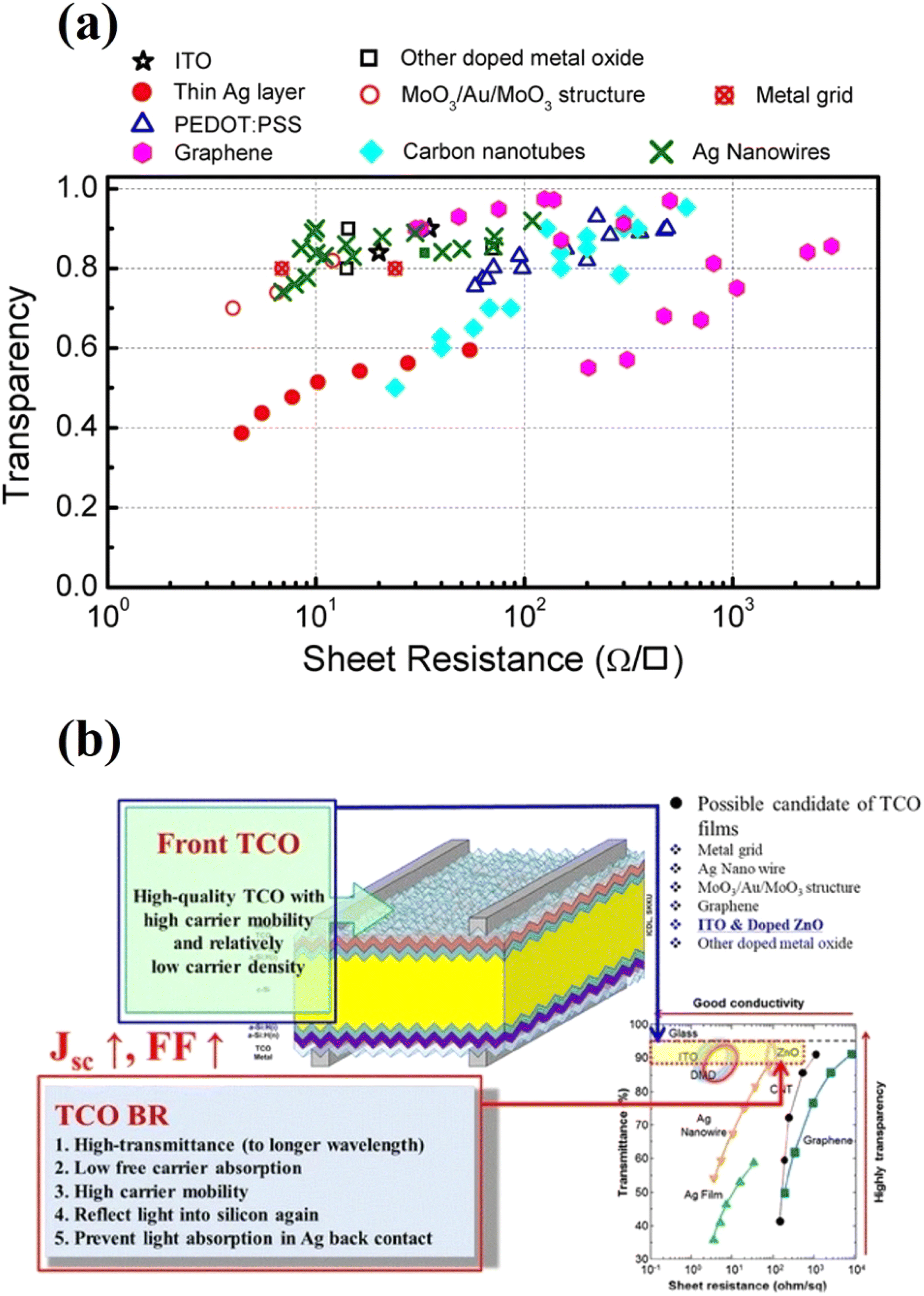 | ||
| Fig. 16 (a) Requirements of TCO layer on SHJ solar cell and possible candidate of front and rear TCO layers (reproduced from ref. 160 with permission from Society of Photo-Optical Instrumentation Engineers, copyright 2014). (b) Reported different types of transparent conductive materials that have been used as transparent electrodes in SHJ solar cells, and the transparency values in the visible spectrum as a function of sheet resistance for transparent conductive materials (reproduced from ref. 161 with permission from American Institute of Physics copyright 2017). | ||
High thermal elasticity and low temperature coefficient are important features of frontal contact solutions for photovoltaics. To understand the importance of thermal effects, we refer to a simple built-in junction potential model in semiconductor engineering that is suitable for idealized mutant p–n junctions. The JSC of SHJ solar cells depends on the range of the built-in voltage Vbi between the a-Si:H(i) layer and c-Si as a charge separation and extraction mechanism, but this may be hindered by the high chip resistance of the TCO. The maximum voltage that a solar cell can provide (Vbi = VOC) is affected by the rate of generation of excess electrons (Δn) or holes (Δp) in the active region where optical transparency before contact is critical,172 we need to maintain maximum optical transmittance to achieve maximum light absorption:
 | (24) |
Commonly used wide bandgap TCO materials are Sn doped In2O3 (ITO),146,154 Al doped ZnO (AZO),117,173–177 Ga doped ZnO (GZO),178 which provide n-type conductivity. Currently, AZO and GZO are promising alternatives to ITO for thin-film transparent electrode applications, where the best candidates for AZO are inexpensive, non-toxic AZOs with low resistivity of about 10−4 Ω cm. The effect of actual absorber conductivity on lateral transport of high and low doping absorbers can be used to evaluate the potential of AZO as a TCO and redesigned to reduce one-dimensional losses.174,176 However, like the problem with the commonly used TCMs, the optical transmittance of doped ZnO is generally low, especially in the NIR spectral range.175 Besides, these metal dopants are highly diffusive: the diffusion of the dopants into the semiconducting active layer of optoelectronic devices severely deteriorates the device performance.
There are many X-doped In2O3 (such as W, Sn, Ce) materials used in SHJ improve performance a lot. Fluorine- and tungsten-doped In2O3 (IFO, and IWO) are found to be favorable for p-contact and n-contact, respectively. While for ITO, it can work well in both p-contact and n-contact, but thinner ITO shows lower contact resistance in p-contact, although its sheet resistance becomes higher. Delft University of Technology and Nankai University have designed and manufactured preferred bifacial SHJ solar cells.179 By applying an IWO 25 nm thick on the front of the device and an ITO 25 nm thick on the back, >22% front-end efficiency was obtained. This represents a 67% reduction in TCO compared to a reference bifacial solar cell with a TCO thickness of 75 nm on both sides. In addition, utilizing the modified SHJ solar cell precursor and further TCO adjustment, our champion bifacial SHJ solar cell had a positive efficiency of 22.84%. The bifacial factor is 0.95. Indium oxide doped with transition metal: IMO, M is the abbreviation for titanium oxide (TiO2), cerium oxide (CeO2) and tantalum oxide (Ta2O5), Such IMO:H films have high carrier mobility over 70 cm2 V−1 s−1, high transmittance, and low free carrier absorption, which leads to a high short circuit current density exceeding 40 mA cm−2. In addition, the low sheet resistance and contact resistivity of the IMO:H films contribute to the high fill factor of the solar cell. And a certified efficiency up to 25.26% (total area, 274.5 cm2) was achieve.180 With the development of TCO, the efficiency of silicon heterojunction solar cells continues to improve, such as IZO181 (Eff = 24.02%), ICO35 (Eff = 26.81%). Developing cost-effective TCO can largely solve the problem of high cost of heterojunction solar cells. Some research institutions use multi-layer TCO consisted of cost-effective TCO and dopped In2O3 to manufacture solar cells, which reduce the use of large amounts of In, such as AZO/IMO (Eff = 25.26%).180
Some research institutions employ sol–gel techniques to cultivate ZnO films, resulting in the successful substitution of ITO in highly efficient optoelectronic devices. As a result, the ZnO film achieves a record high conductivity of close to 500 S cm−1 and ultra-low optical absorption losses (<1% at wavelengths over 400 nm).176 Tang et al.182 used ITO/AZO/ITO at front and AZO at rear side in M2+ solar cells, which finally achieved a champion efficiency of 23.8% with >85% indium reduction. This research result reduces a large amount of In used in SHJ, provides a strategy for the development of SHJ in the future. In addition to the preparation of different oxide materials, the idea of oxide stacking is also important. Compared to single-layer ITO, multi-layer structure reduces the use of In, provides sufficient raw materials, and is more environmentally friendly.
SnOx can not only be used as an electron transport layer (ETL), but also SnO-based thin films play an important role in SHJ devices as a TCO for SHJ cells. Suzhou Maxwell Technologies successfully prepared cheap and mass-producible35 (SnOx) electrode materials by sputtering at room temperature, which is applied to the SHJ, achieving a maximum efficiency of 24.91%. Finally, SHJ solar cells with plating copper electrode and double-side IMO:H/SnOx transparent electrodes were prepared, and a certified efficiency of 25.94% (total area of 274.4 cm2) was achieved, and the amount of In was reduced by 50%.36 Reactive plasma deposition is utilized by AIST to prepare a-SnO2 thin films that are appropriate for solar cells. These films exhibit good electrical conductivity and high moisture and heat stability, while maintaining high transparency in the visible and near-infrared regions.183 When the a-SnO2 layer was applied to the SHJ solar cell, it was observed that the TCO layer had almost no negative impact on the performance of the SHJ, as compared to the solar cell with the indium tin oxide layer. Commonly used TCOs are summarized in Table 4.
| No. | Material | Type | V OC (mA) | J SC (mA cm−2) | FF (%) | E ff (%) | Ref. |
|---|---|---|---|---|---|---|---|
| 1 | ICO | n-type | 751.4 | 41.30 | 86.07 | 26.81 | 35 |
| 2 | IMO:H | n-type | 746.2 | 40.10 | 84.64 | 25.26 | 180 |
| 4 | AZO | n-type | 747.5 | 39.13 | 86.23 | 24.94 | 180 |
| 5 | BZO | n-type | 628 | 41.76 | 67.80 | 17.79 | 184 |
| 6 | IZO | n-type | 743.7 | 38.35 | 84.22 | 24.02 | 181 |
| 7 | IWO | n-type | 731.0 | 40.16 | 78.07 | 22.92 | 185 |
| 8 | AZO/IMO:H | n-type | 747.4 | 40.10 | 85.48 | 25.26 | 180 |
| 9 | ITO | n-type | 747.0 | 39.60 | 84.90 | 25.20 | 186 |
| 10 | IO:H | n-type | 612 | 34.26 | 76.70 | 16.06 | 187 |
| 11 | ZnO/AZO | n-type | 645.3 | 37.11 | 71.60 | 17.13 | 117 |
| 12 | Al2O3/IZO | n-type | 740.0 | 40.53 | 72.33 | 21.57 | 177 |
| 13 | GZO | n-type | 741.5 | 38.79 | 82.56 | 23.65 | 178 |
| 14 | a-SnOx | n-type | 714.0 | 39.30 | 78.90 | 22.18 | 183 |
| 15 | SnOx | n-type | 747.7 | 39.60 | 84.14 | 24.91 | 36 |
| 16 | SnOx/IMO:H | n-type | 747.5 | 40.49 | 85.71 | 25.94 | 36 |
| 17 | SnO:Ta | n-type | 748.8 | 39.98 | 83.83 | 25.10 | 188 |
At present, the silicon heterojunction (SHJ) cells employ indium-based transparent conductive oxide (TCO) layers to support lateral carrier transport (refer to part 6.1 for details). Nevertheless, In is a typical rare metal. For sustainable production, its consumption in solar cell manufacturing must be minimized. Researchers have developed TCO-free SHJ solar cells. For instance, Li et al.189 achieved an SHJ solar cell with an efficiency of over 22% without TCO front contacts (Fig. 17a). The absence of the TCO front contact enhanced the external quantum efficiency. He et al.190 realized an efficient heterojunction solar cell without conductive oxide through rational utilization of non-dopant contacts. Compared with the work of Li et al., He et al. used non-doped TiOx/RbFx and MoOx as the front and rear contact points on the n-side and p-side, respectively. MoOx/Ag back-contact was used for hole-selective contact and RbFx/Al front contact for electron-selective contact, and ultimately an efficiency of 22.9% was obtained, as shown in Fig. 17b. Hitoshi Sai et al.191 conducted a detailed study on the influence of the TCO layer on electrical transport and stability. The research findings indicated that, regardless of the wafer polarity, the single-face rear-junction structure is beneficial for effectively collecting minority carriers without the aid of the TCO layer. The contact resistivity in the local metallized region must be minimized to achieve effective carrier transport. Correspondingly, a TCO-free SHJ cell with an efficiency of 22.1% was demonstrated in Fig. 17c.
 | ||
| Fig. 17 (a) Sketch of SHJ solar cell structure with a rear emitter and both sides TCO-free contacts (reproduced from ref. 189 with permission from Cell Press, copyright 2021). (b) Enabling TCO-Free efficient heterojunction solar cells by flexibly using dopant-free contact (reproduced from ref. 190 with permission from Wiley, copyright 2022). (c) EQE spectra of all TCO-free, front-TCO-free, and conventional SHJ cells (reproduced from ref. 191 with permission from Wiley, copyright 2023). | ||
Due to the absence of the TCO layer, compared with conventional SHJ, TCO-free solar cells still exhibit a considerable domain in terms of efficiency and stability. High-efficiency TCO-free SHJ solar cells are feasible and TCO-free SHJ technology can reduce the device cost. However, direct contact between Ag/a-Si:H may potentially lead to the penetration of Ag into the a-Si:H layer, thereby causing a device performance reduction. Overall, TCO-free SHJ technology remains in the exploration stage.
5.2 Metallization technology
The most pressing challenge currently hindering the expansion of SHJ solar cell industry is the relatively high cost of production. The low-temperature silver paste used in the SHJ process accounts for about 30% of the total processing cost due to its high consumption.172 Therefore, many institutions are also very interested in the improvement of metal electrode materials and technologies. To improve the conductivity of electrodes and reduce the metallization cost, multi-busbar, fine-line printing, and low-temperature-cured silver-coated copper pastes have been developed.192 In addition, several potential metallization technologies for SHJ solar cells, such as the smart wire contacting technology,193 pattern transfer printing,194 inkjet/FlexTrail printing,195 and copper electroplating.36,43,196,197A larger amount of low temperature silver paste for better ohmic contact is required, which will significantly affect the cost of SHJ solar cells.198 Thus, lower silver paste consumption or substitution of expensive silver paste is of high demand for SHJ solar cell. Copper plating aroused great interest and is regarded as an ideal alternative electrode solution and industrially proven technology.43,196,197 Benefited from the copper's high conductivity and thin finger width, the shading loss and finger resistance can be reduced remarkably, which can enhance the electrical properties. For example, SiNX film acts as anti-reflection coating and plating mask, Ni–Si alloy as copper diffusion barrier.196
The resistivity of copper-plated electrode is close to bulk copper material, which is 2–3 times lower than printed silver electrode and could achieve decreased contact resistance and finer line. The surface morphologies comparison of printed finger and copper plated finger are shown in Fig. 18. The printed silver finger is unsmooth and wide. The topography image shows that the screen-printed Ag finger is triangular. Low temperature silver paste fulfilled with hundreds of nanometers' voids has also been observed in the cross-sectional SEM image. Taking advantage of the photolithography based, the copper finger width can be less than 30 μm. The plated copper finger is compact and uniform. Its cross section is rectangular and the surface roughness is less than 2 μm. However, the existing TCO layer makes the copper metallization totally differ from the process in diffused-emitter solar cells. The plating methods applied in diffused-emitter solar cell, such as laser ablating SiNx film,200 light induced plating (LIP). The current research progress in electroplating of SHJ solar cells with different methods are summarized in Table 5.
 | ||
| Fig. 18 SHJ solar cells: (a and c) with screen printed finger, (b and d) with electroplated finger (reproduced from ref. 199 with permission from Elsevier, copyright 2023). The electroplated one is thinner than the screen printed one, which reduced the amount of silver paste by 50%. | ||
| Deposition method | Finger width (μm) | E ff (%) | Ref. |
|---|---|---|---|
| Low-temperature-cured | — | 25.11 | 47 |
| Inkjet printing | 23.3 | 195 | |
| FlexTrail printing | 23.7 | 195 | |
| Electrode on seed | 30–40 | 25.10 | 33 |
| Ni/Cu light induced plating | 15 | 22.4 | 201 |
| Pulse reverses current plating | 30–40 | 20.2 | 202 |
| Reverse pulse plating on Ni seed | 30 | 22.2 | 203 |
| Cu–Ni alloy palting | — | 22.5 | 196 |
| Electrode on PVD Ag seed | — | 19.4 | 197 |
| PVD copper plating | 9 | 26.41 | 43 |
| Laser transfer printing | 18 | 26.81 | 35 |
The challenges faced by the copper metallization process of SHJ solar cells are mainly the selective plating of TCO film and the adhesion of the metal oxide layer. The long-term reliability of electroplated solar cells is another decisive factor in determining whether copper metallization can be mass-produced.153,155,157 For copper metallization of conventional solar cells with diffusion emitters, nickel is electro/chemically deposited. Nickel–silicon alloys are formed during subsequent annealing as a copper diffusion barrier layer In the TCO film category, ITO films with a thickness of 10–60 nm were tested as copper barriers with a maximum failure temperature of 750 °C.156,158,204,205 The difference in adhesion between the direct plating electrode and the TCO is one of the main challenges in simplifying the plating process, but improved adhesion of 3–5 N mm−1 can be achieved through the intermediate seed layer,72,76 Copper metallization must face competition from new module technologies. The combination of fine wire screen printing and multi-busbar interconnection (or Meyer Burger's Smart Wiring Technology (SWCT)) can significantly reduce the consumption of silver paste, resulting in a consumption of silver paste as low as 100 mg.206–208 Electroplating technology must demonstrate its cost-effectiveness advantages, otherwise breakthroughs in mass production will not be achieved. In addition to single-element metals as seed layers, co-deposited metal alloys are also deposited as electroplated seed layers. On the same ITO film, the contact resistivity of Cu–Ni alloy (0.6 mΩ cm2) is lower than that of the evaporated copper seed crystal layer (1.18 mΩ cm2), resulting in SHJ solar cells with a fill factor of 77.4% and conversion efficiency (22.5%).196
Although much effort has been currently performed in transferring the SHJ solar cell technology to high-volume manufacturing, metallization is still one of the toughest factors slowing down its industrialization progress.198,209 Metallization not only affects the electrical performance and cost of SHJ solar cells but also affects the long-term reliability of SHJ module products.210 More than that, due to the large particles of low-temperature silver paste, the traditional printing method of fine rasterization is very difficult, and with the continuous development of the industry makes the use of silver paste come to a new stage. Pattern transfer printing (PTP)194 or laser transfer printing technology (LTP),203 a contactless printing technology by Utilight, has a fine finger less than 20 μm, which can deposit the finger width smaller than that, as shown in Fig. 19.
 | ||
| Fig. 19 (a and b) SEM images of a finger smaller than 20 μm deposited by PTP. (c) Schematic diagram of the working principle of PTP (reproduced from ref. 194 with permission from Elsevier, copyright 2015). | ||
The main advantages of LTP are as follows:(i) LTP has a smaller finger, which can reduce the cost of silver paste more than 30%, Adrian et al. Compared with the screen printing and LTP, the amount of silver required reduced by 54%;211 (ii) LTP technology has excellent consistency and can keep the error within 20 μm, even can be used in the low-temperature-cured silver paste; (iii) the LTP is a contactless technology, which can avoid the problems of hidden cracks, broken pieces, contamination, scratches, etc. that exist in extrusion printing. Solar cells get thinner in recent years, LTP technology can effectively reduce the amount of silver paste used, and its damage to the cell is less because the contactless printing method. In October 2023, LONGi used the laser transfer technology to make the front finger on industry-grade silicon wafers, it has improved JSC dramatically, which resulted in the record efficiency 26.81%,35 and in October 2024, silicon heterojunction back contact solar cells by laser patterning reached a champion efficiency of 27.30%.21
In summary, screen printing is still the mainstream solution, and further technological upgrades are needed for screen printing to achieve ultra-high utilization of Ag. The application of copper plating to silicon photovoltaics, especially in the field of silicon heterojunction, has important practical significance. However, the complex heterojunction solar cell plating process is the biggest obstacle to its industrialization. Selective deposition of seed layers and peel-free resists are key factors in simplifying the electroplating process. More innovative research is needed to break through the shortcomings of existing technologies. The development of non-destructive laser technology combined with inorganic graphics processes shows the potential for low-cost mass production of copper metallization. In the efficiency of LONGi's SHJ solar cells, traditional electrode growth methods are difficult to achieve higher efficiency, and laser transfer printing methods need to be given our attention. Although many constraints and challenges still need to be addressed, new metallization technologies should also be highlighted to disburden the current limitations of screen-printing metallization and pave the way for further efficiency increases and cost reductions in SHJ solar cells and modules.
6. Modified structure for SHJ solar cells
6.1 Rear emitter structure
As a design of standard (metal/TCO/a-Si:H(p)/a-Si:H(i)/c-Si(n)/a-Si:H(i)/a-Si:H(n)/TCO/metal) structure at soaked front is strongly dictated by the parasitic absorption in the SHJ layers, a-Si:H layer and TCO, optimization of the front layer stack is tricky as it comes at the cost of open-voltage (VOC) and fill factor. Furthermore, the performance of the solar cell depends on the carrier collection of doped amorphous silicon (a-Si) layer, passivation quality of intrinsic a-Si layer, and TCO properties. Fundamental issues such as increment of the junction recombination with high doping a-Si:H layers and Schottky barrier of p-type a-Si:H with the n-type TCO's are an upper limit of VOC and a trade-off between VOC and FF and JSC and FF, respectively. Fig. 20 shows a schematic of standard emitter and rear emitter SHJ solar cells. | ||
| Fig. 20 Schematic diagram of the structure of the solar cell after the emission junction (a) schematic of a rear emitter structure and (b) front emitter structure (c) (Top), sketch of simulated and experimentally investigated cell structures. (Bottom) simulated current density within the absorber for MPP conditions indicating that a large part of the lateral transport is shifted from the TCO (not visible) into the absorber. The series and parallel connection between the absorber and the TCO for the FE and RE design is indicated as well (reproduced from ref. 212 and 213 with permission from Elsevier and The Korean Institute of Electrical and Electronic Material Engineers, copyright 2014 & 2020). | ||
High FF could be obtained with rear-emitter structures. Certainly, on n-type wafers, photo-generated electrons can benefit from the high lateral conductivity to be extracted towards the contacts.214,215 Rear-emitter SHJ solar cells are attractive because of the lateral conductivity of electrons through the wafer yielding a higher fill factor than conventional front emitter structures.212 However, minority carriers being collected at the rear of the cell, they are more sensitive to recombination at the front interface as there is no p–n junction induced electric field to separate charges. If the rear-emitter layer become too thin, there are no field effect passivation anymore and the interface is highly recombination. Silicon heterojunction solar cells having a rear-emitter structure feature thin silicon amorphous layers (a-Si:H) enveloping the c-Si substrate. Owing to the high-quality passivation of a-Si:H layers, SHJ solar cells can achieve easily high VOC, but achieving simultaneously a high fill factor on large area cells remains challenging.213,216 Now, Table 6 has a brief outline cell performance by comparing front emitter versus rear emitter regarding the transport mechanism and current flow. In conventional front emitter (FE) cells, the minority carriers of the holes are subjected to lateral transport toward the front metal grid electrode. In this configuration, the front side TCO and the absorber are horizontally p/n junction, resulting in a series connection of the absorber and the TCO.212 At the p/n junction, holes are separated from the absorber and the actual barrier formed by the p/n junction prevents the back diffusion of the absorber.
| FE | RE | |
|---|---|---|
| Transport mechanism | 2D transport loss (high/low junction, p/n) | 1D transport loss |
| Current flow | Lateral and vertical conductivity | Lateral conductivity |
Rear emitter (RE) devices are subjected to lateral transmission from absorber (electronic) carriers to metal grid electrodes. In this case, the front TCO and absorber are coupled horizontally through a high/low junction, connecting the TCO and absorber in parallel. This fact can be achieved within the absorber grid electrodes, with more favorable current flow patterns for carrier collection. When the device is designed with RE instead of FE, the current density inside the absorber is higher and the transverse portion of the current within the absorber is more pronounced. Therefore, in the RE design, a significant portion of the lateral current is transferred from the front-end TCO to the absorber. This results in less stringent restrictions on lateral transmission within the front-end TCO, which is why for RE designs, the influence of the thin layer resistance of the TCO electrode and the spacing of the gate electrode on the FF can be largely decoupled.212,217
To overcome parasitic absorption in standard a-Si:H/c-Si heterojunction solar cells, Wünsch218 obtained an inverted a-Si:H/c-Si cell by designing a heterojunction on the back of a solar cell. The p–n junction of this cell is located on the back, and no light passes through the a-Si:H(p) emitter, so its thickness does not have to be as thin as possible, but only optimized from the perspective of minimum interface recombination speed and maximum open-circuit voltage. In addition, more conductive layers can optionally be deposited on the a-Si:H(p) emission layer to improve band bending at the a-Si:H(p)/n-c-Si interface, without necessarily being a transparent TCO film. Solar cells of this structure appear with relatively low initial efficiency, only 11.05%, but it gave people great inspiration to make SHJ cells with emitters on the back.
In Fig. 20b, it is possible to reduce power losses due to 2D transmission by placing high/low junctions at the front end and p/n junctions at the back end by placing high/low junctions on the front end and p/n junctions at the back end. The lateral conductivity of the absorbing material can open additional transmission paths. The electrical volume characteristics of optics and TCO are less pronounced, which means that requirements for spacing, TCO mobility, or free carrier density are lower. The reduced free carrier density allows for higher JSC without affecting FF (and vice versa), resulting in higher efficiency. This can be interpreted as the transfer of the transverse transmission section from the TCO to the absorber. In terms of 2D effects, this distinguishes the rear emitter (RE) design from the traditional front emitter (FE) design and provides more freedom in device design. Equipped with a more complex p-type doping in the unilluminated rear, it is possible to focus on optimizing its electrical performance, while the n-type doping at the front makes the trade-off between optical and electrical performance less stringent. The results show that at the high/low junction, additional transport through the absorber facilitates lateral carrier transport and the transverse conductivity of TCO decreases. This means that under MPP conditions, the voltage drop in the TCO electrode is low, this reduces ohmic losses and non-generation losses. Although the a-Si:H/c-Si heterojunction cell with the emitter on the back can theoretically reduce parasitic absorption and is conducive to the improvement of cell efficiency, there is still a certain gap between its efficiency and that of standard SHJ cells, so it needs to be continuously studied and optimization.
6.2 Interdigitated back contact structure
Apart from shadowing losses due to current collecting grids at the front side, short wavelength response losses are inevitable in front heterojunction solar cells due to parasitic absorption caused by a-Si:H films/TCO. Both issues cause reduction in JSC. These two issues can be avoided by employing contacts as interdigitated pattern. In 2014, Sharp first proposed an HBC solar cell with a conversion efficiency of 25.1%.40 Almost simultaneously, Panasonic achieved a higher conversion efficiency of 25.6%, with a design area of 143.7 cm2, breaking the efficiency record of crystalline silicon-based solar cells at the time.219In mid-September 2016, Kaneka Corporation announced a conversion efficiency of 26.3% for HBC solar cells with a designated area of 180.4 cm.32 Soon, HBC solar cells based on n-type c-Si wafers have a size of 243 cm2, a thickness of 200 μm, and a resistivity of about 7 Ω cm, which achieve a high conversion efficiency of 26.6%.220 The IBC design is particularly attractive because it does not require a functional contact stack on the front of the device, which frees up design space for highly transparent materials. In general, however, IBC designs introduce greater manufacturing complexity into other simple SHJ unit processes, an issue that is currently being actively investigated.45 In addition, the current crowding effect close to the back contacts reduces radiated recombination.221 IBC solar cells achieve high short-circuit currents by eliminating metal grid shading on the front surface. In IBC designs, both electron and hole collection occur at the back side of the device. This allows a high degree of freedom in the optical and electronic design of the front of the solar cell, with a JSC of up to 42.7 mA cm−2.172 IBC solar cells generally have higher absorption and short-circuit current densities. Other advantages are as follows: (i) since there is no front metal finger, there is no need to consider the contact resistance on the front side, which provides more space and potential for optimizing the passivation performance of the front surface; (ii) since the shading loss of the front metal finger is not considered, a wider finger can be used to reduce the series resistance of the rear metal contact; (iii) the design of all rear contacts makes the interconnection of units in the module simpler and more aesthetically pleasing.
Some research groups have used Silvaco Atlas tools for the design of emitters and BSFs for simulations and experiments. As shown in Fig. 21, with and without intrinsic a-Si:H passivation layers for doped emitters and BSFs. It was found that in order to avoid recombination at the rear, the BSF size should be less than half of the emitter size of the distance between the same polarity, i.e. emitter to emitter or BSF to BSF, called pitch size is also an important factor in high efficiency.222
 | ||
| Fig. 21 (a) An interdigitated electrode pattern (current collecting girls) at the rear side of the c-Si wafer (b) probability of minority carrier recombination is enhanced when emitter size is a smaller than BSF size (figure not to scale) (c) emitter in direct contact with c-Si (d) BSF in direct contact with c-Si (peproduced from ref. 222 with permission from Springer, copyright 2017). | ||
The key problem for IBC solar cells is how to prepare n-regions and p-regions with good quality and sympathetic distribution on the posterior surface. In recent years, ion implantation technology has been applied to IBC solar cells because the technology can precisely control the doping concentration to obtain uniform p-region and n-region with controllable junction depth. However, the introduction and activation of dopants requires a high annealing temperature, which is a difficult problem in the photovoltaic industry.219,223 Compared with conventional crystalline silicon cells, surface recombination of the front surface has a greater impact on the performance of IBC solar cells because the front surface is far away from the p–n junction located on the back side. In order to inhibit front surface recombination, a better surface passivation scheme is required for the front surface. At the same time, high-quality substrate materials with long diffusion lengths are often required to ensure that the minority of carriers produced by photons do not recombine before reaching the posterior junction. At the rear side, the grid lines are separated by 10 μm and the area within the electrodes are filled by contact metal in the rear side layout.
7. SHJ-based tandem solar cells
To break through the Shockley–Queisser limit of single-junction solar cells and obtain more efficient photovoltaic devices, tandem solar cells (TSC) have attracted widespread attention.224 In multi-junction or tandem solar cells, the top cell has a wider band gap that can absorb high-energy photons. Tandem solar cells based on silicon heterojunction bottom cells, such as perovskite PVK/Si and III–V/Si tandem solar cells, are growing fast. As early as 1985, Yablonovitch et al. pointed out that an ideal solar cell should have a double heterojunction structure; that is, an absorber material with a smaller bandgap is placed between two materials with a broad bandgap with different doping types. The structure is easy to obtain with large quasi-Fermi level splitting in the absorbing layer material. High voltage and efficiency can be obtained if the heterojunction interface can be well-passivated. SHJ solar cells have the advantages of a simple and symmetrical structure and a low process temperature.225 In addition, SHJ solar cells have a unique energy band structure and full-area passivation. In TSCs, SHJ cells have some natural advantages as bottom cells, the SHJ structure contains TCO material as a natural tunnel junction, which also makes the SHJ more suitable as a bottom cell. However, it is a challenge to grow high-quality perovskite films on a fluted heterojunction bottom cell.226As for the PVK/Si tandem cells, there are two mainstream designs of PVK/Si tandem solar cells: two terminal (2T) and four terminal (4T) structures.227 2T device may offer some efficiency advantages over the parasitic absorption losses of the two ultra-transparent electrodes of a 4T structure. However, the fabrication of 2T devices poses more technical challenges in terms of materials and device structure. Perovskite solar cells as top sub-cells are particularly suitable for forming 2T TSCs with c-Si bottom sub-cell to absorb a larger solar spectral range because their band gap is adjustable.228 For example, the high-temperature annealing process required for selective contact of certain inorganic carriers can be detrimental to the passivation and contact quality of the bottom subcell.
Compared with perovskite materials, III–V compound semiconductor materials, with their excellent proven reliability and adjustable band gap, exhibit high efficiency and promising potential for industrial application.229 Epitaxial growth method is an advanced technology to obtain high quality multilayer films, but it has strict requirements on substrate and thin film growth. These characteristics make III–V solar cells expensive and limit the application of III–V//SHJ tandem solar cells.230 The current maximum efficiency of PVK/SHJ tandem solar cells is 34.6%,231,232 and the maximum efficiency of III–V//Si is 36.1%.233 Typical PVK/SHJ and III-V//Si tandem solar cell devices are shown in Fig. 22.233,234 Generally, tandem solar cells based on silicon heterojunction bottom cells, such as PVK/Si and III–V/Si tandem solar cells, are under development. Relative review of Si based tandem solar cells can be referenced in recent articles.235–238
 | ||
| Fig. 22 (a) Schematic of the monolithic perovskite/silicon tandem solar cell built from a double-side-textured SHJ cell and (b) J–V curve and the maximum power output point of one PVK/SHJ tandem cell, measured by NREL using the asymptotic maximum power scan method (reproduced from ref. 234 with permission from Springer Nature, copyright 2024). (c) Schematic structure of the III–V//SHJ triple-junction solar cell with 36.1% efficiency and (d) J–V curve of III–V//SHJ solar cell (reproduced from ref. 233 with permission from Wiley, copyright 2024). | ||
8. Industrialization of SHJ solar cells
SHJ solar cells consist of only five steps in industrial production compared to other types of solar cells. Fewer steps, low temperature, and less energy consumption are the advantages of SHJ solar cells.14 As shown in Fig. 23, the manufacturing process of typical SHJ solar cells begins with wafer cleaning and alkaline texturing, followed by PECVD to form a single-sided intrinsic and doped a-Si:H stack and then opposite polarity on the other side. Next, the front and back of the cell are covered by PVD by applying a TCO layer, and then metal electrodes are formed by PVD, screen printing or electroplating, fabrication process steps of double-side contacted SHJ solar cell, as well as the schematic diagrams of IBC-SHJ and bifacial SHJ solar cells have shown in Fig. 23. | ||
| Fig. 23 Fabrication process steps of double-side contacted SHJ solar cell, as well as the schematic diagrams of IBC (interdigitated back contact) SHJ and bifacial SHJ solar cells (reproduced from ref. 14 with permission from Springer Nature, copyright 2019). | ||
Since 1997, when Sanyo introduced the SHJ industrial line, the SHJ industrial line has been continuously updated. Considering the high bifacial coefficient (>90%), low temperature coefficient and high energy yield, SHJ has the potential to achieve ultra-low power costs, and thinner wafers can reduce costs. Many of the technical aspects we discuss here are as follows:
(i) Passivation uniformity problem: a major difficulty is to achieve a uniform ultra-thin passivation layer based on a-Si:H in PECVD. In fact, these problems can be solved, for example by carrying out PECVD reactor design.41,239 (ii) Wafer selection issues: current SHJ use more expensive n-type wafers that are less sensitive to gap transition metal defects present in the feedstock, reducing refining costs. While p-type silicon currently accounts for the majority of the market, most monocrystalline silicon manufacturers have developed proprietary technologies that enable them to grow high-quality n-type silicon (lifetime/resistivity typically greater than 1 ms Ω−1 cm−1) at a similar or only slightly higher cost to p-type materials.240,241 (iii) TCO cost problem: usually 100 nm ITO is deposited in the front and back of SHJ. ITO targets are a major cost factor, using about 3.5 g of indium per square meter (considering the 50% sputtering material usage). For TCO replacement, new materials such as ZnO and SnO2 can be selected, especially on the n-side, where wafer conductivity plays a major role. (iv) The problem of high metallization cost: since the final annealing step is around 200 °C, a low curing temperature silver paste is used.193,198 Due to the use of a multi-wire configuration, in which the strip is replaced by a round wire, the need for seeker conductance is further reduced: typical 18 wires ∼ 300 μm, embedded in a polymer foil, soldered to soft silver paste during lamination. Due to the short distance between the two wires, it is possible to reduce silver consumption to 10–20 mg on each side of 6 inches. To completely curb the demand for silver, copper plating was also reported as an alternative, and the process of directly achieving double-sided copper metallization was also shown above.242 The process has low-cost potential after large-scale acceptance. In addition, optimizing grid configurations using industry-compatible contact-free laser transfer printing (LTP) technology can improve solar cell efficiency, which can have a huge impact on reducing manufacturing costs.203
The main reasons for the decrease in SHJ solar cell cost are (i) high module efficiency (>24%), (ii) better temperature coefficient (∼0.21%/°C) indicating less performance loss over their cycles, and (iii) lower manufacturing temperatures. For every approximately 1% increase in module efficiency, the system cost balance is reduced by about 6–7%.243 With a better temperature coefficient, SHJ cells can get higher solar energy during the day and throughout the year, which makes the technology particularly attractive for hot climate markets. Due to its higher conversion efficiency and good rear contact IR reflection characteristics, this will also significantly reduce device heating compared to the diffusion junction method. In addition, frameless designs are being explored to further improve the cost-effectiveness of SHJ cells. For standard solar glass, the phenomenon of unnecessary light loss is reflected by a refractive index mismatch at the glass/air interface, about 4%. Some measures need to be taken to improve the utilization of light. For instance, it is found that the industrial sol gel process is used to apply the porous SiO2 layer to the glass, thus increasing the JSC by about 2.7%.244
In industrial production, for standard industrial production lines, reducing wafer thickness is feasible to enable low-cost solar cells, and flexibility is a decisive advantage in applying silicon solar cells to life, such as power supplies for wearable devices and building-integrated photovoltaics (BIPV). Using 50 μm thick silicon wafers can save more than 70% of silicon material costs. However, the efficiency is limited due to insufficient light absorption on ultra-thin silicon substrates, especially in the long-wave region. Nanostructures are an effective method of light harvesting. For example, a 10 μm-thick inverted nanopyramid silicon achieves effective solar cell light absorption.245
PV industries are shifting from aluminum back surface field (Al-BSF) c-Si to passivated emitter and rear cell (PERC) and SHJ to increase efficiency further. Fig. 24 presents the projected world market share for different silicon-based PV technologies. According to the ITRPV (2023),246 at present, PERC still holds over 70% of the c-Si market share, it is noted that the traditional Al-BSF is predicted to be outdated in 2025, while PERC, SHJ, IBC, and Si-tandem solar cells will be increased in the future, and TOPcon is expected to become the dominating solar cells after 2025.247 Like PERC, TOPCon and HJT (SHJ) are expected to become mainstream PV technologies in the next two to three years, as these technologies offer significant advantages in terms of cost control, raw material availability, ease of process and high efficiency. The primary advantage of TOPcon solar cells, as compared to SHJ solar cells, is their compatibility with current PERC production lines. TOPCon cells are based on the PERC process, with the addition of a tunneling oxide layer and a polycrystalline silicon layer, which makes upgrading the production line easier. SHJ, on the other hand, is one of the newest crystalline silicon PV technologies, and large-scale production requires updates for new equipments. Therefore, solving the production cost problem of SHJ is crucial for making it commercially available.
 | ||
| Fig. 24 Global market share for different solar cell technologies.246 | ||
9. Summary and outlook
This review provides a comprehensive overview of all aspects of SHJ solar cells, from basic theory to intrinsic passivation layer and other material selection, as well as related series of devices. SHJ solar cells are currently at the forefront of silicon solar cell research in terms of conversion efficiency. Through the introduction of passivation and stack processing in the contact layer elements, enhancements are made to carrier selectivity, passivation quality, transparency, and conductivity. It is expected to increase the efficiency limit of single-junction silicon. Due to the successful development of the passivated contact layer, the efficiency of SHJ solar cells has exceeded 27%, showing the great potential and development space of silicon heterojunction technology. Then through further improvement of TCO materials and the design of corresponding emerging thin film structures, the limit efficiency of single-junction silicon cells can be further approached.While diffusion homojunction silicon solar cells such as Al-BSF and PERC currently dominate the PV market, SHJ solar cells will become the next generation of high-efficiency PV products. Despite of the notable achievements, the large-scale commercialization of SHJ technology remains very challenging. The SHJ solar cell industry line does not match the existing conventional production line, the main obstacle to commercialization is the big capital required to build the production line and reduce the cost of the main thin-film fabrication tools (like PECVD and PVD). Manufacturers should accelerate technological transformation (like IBC-SHJ soar cells) to realize larger scale industrialization. With the manufacture of high-efficiency devices, the use of indium and silver should be reduced (or even completely avoided). Low-cost metalized materials (like Al and Cu pastes and Al grids) should be developed to further reduce costs. Hope that there will be no material resource limitations for TW scale production for SHJ solar cells. More efficient SHJ-based tandem solar cells (like PVK/SHJ and III–V//SHJ) are the future development direction. We believe that this review will help to understand the remaining challenges and possible research directions, and promote faster development of the field.
Data availability
Data availability is not applicable to this article as no new data were created or analyzed in this study.Conflicts of interest
There are no conflicts to declare.Acknowledgements
This work is supported by the National Key Research and Development Program of China (No. 2022YFB4200102), and Tianjin Natural Science Foundation Project (No. 21JCYBJC00270).References
- W. Duan, A. Lambertz, K. Bittkau, D. Qiu, K. Qiu, U. Rau and K. Ding, Prog. Photovoltaics Res. Appl., 2021, 30, 384–392 Search PubMed.
- D. Moore, S. Krishnamurthy, Y. Chao, Q. Wang, D. Brabazon and P. J. McNally, Phys. Status Solidi A, 2011, 208, 604–607 Search PubMed.
- P. H. A. Veríssimo, R. A. Campos, M. V. Guarnieri, J. P. A. Veríssimo, L. R. do Nascimento and R. Rüther, Sol. Energy, 2020, 211, 433–445 Search PubMed.
- Y. Liu, Y. Li, Y. Wu, G. Yang, L. Mazzarella, P. Procel-Moya, A. C. Tamboli, K. Weber, M. Boccard, O. Isabella, X. Yang and B. Sun, Mater. Sci. Eng., R, 2020, 142, 100579 CrossRef.
- F. M. Orr, ACS Energy Lett., 2016, 1, 113–114 CrossRef CAS.
- J. Haschke, O. Dupre, M. Boccard and C. Ballif, Sol. Energy Mater. Sol. Cells, 2018, 187, 140–153 CrossRef CAS.
- J. Veirman, R. Varache, M. Albaric, A. Danel, B. Guo, N. Fu and Y. C. Wang, Sol. Energy Mater. Sol. Cells, 2021, 228, 11 CrossRef.
- A. Haeri, J. Mater. Sci.: Mater. Electron., 2017, 28, 18183–18192 CrossRef CAS.
- A. Richter, M. Hermle and S. W. Glunz, IEEE J. Photovoltaics, 2013, 3, 1184–1191 Search PubMed.
- J. Ziegler, A. Montesdeoca-Santana, D. Platt, S. Hohage, R. Guerrero-Lemus and D. Borchert, Jpn. J. Appl. Phys., 2012, 51, 4 CrossRef.
- W. Long, S. Yin, F. Peng, M. Yang, L. Fang, X. Ru, M. Qu, H. Lin and X. Xu, Sol. Energy Mater. Sol. Cells, 2021, 231, 111291 CrossRef CAS.
- J. Schmidt, R. Peibst and R. Brendel, Sol. Energy Mater. Sol. Cells, 2018, 187, 39–54 CrossRef CAS.
- Y. C. Zhang, M. Kim, W. Li, P. Verlinden and B. Hallam, Energy Environ. Sci., 2021, 14, 5587–5610 RSC.
- T. G. Allen, J. Bullock, X. Yang, A. Javey and S. De Wolf, Nat. Energy, 2019, 4, 914–928 CrossRef CAS.
- Y. R. Lin, M. M. Feng, Z. X. Wang, Y. H. Zeng, M. D. Liao, L. F. Gong, B. J. Yan, Z. Z. Yuan and J. C. Ye, Sol. Energy, 2020, 211, 753–758 CrossRef CAS.
- Y. Yu, S. Li, F. Xi, H. Lan, D. Wu, Z. Chen, W. Ma and R. Deng, Sol. Energy, 2023, 263, 111938 CrossRef CAS.
- P. A. Basore, Prog. Photovoltaics Res. Appl., 2016, 24, 1024–1031 CrossRef.
- D. B. Needleman, J. R. Poindexter, R. C. Kurchin, I. M. Peters, G. Wilson and T. Buonassisi, IEEE 43rd Photovoltaic Specialists Conference (PVSC), Portland, OR, USA, 2016, pp. 3487–3491 Search PubMed.
- J. Melskens, B. Van de Loo, B. Macco, L. Black, S. Smit and W. Kessels, IEEE J. Photovoltaics, 2018, 8, 373–388 Search PubMed.
- C. Hollemann, F. Haase, S. Schäfer, J. Krügener, R. Brendel and R. Peibst, Prog. Photovoltaics Res. Appl., 2019, 27, 950–958 Search PubMed.
- H. Wu, F. Ye, M. Yang, F. Luo, X. Tang, Q. Tang, H. Qiu, Z. Huang, G. Wang, Z. Sun, H. Lin, J. Wei, Y. Li, X. Tian, J. Zhang, L. Xie, X. Deng, T. Yuan, M. Yu, Y. Liu, P. Li, H. Chen, S. Zhou, Q. Xu, P. Li, J. Duan, J. Chen, C. Li, S. Yin, B. Liu, C. Sun, Q. Su, Y. Wang, H. Deng, T. Xie, P. Gao, Q. Kang, Y. Zhang, H. Yan, N. Yuan, F. Peng, Y. Yuan, X. Ru, B. He, L. Chen, J. Wang, J. Lu, M. Qu, C. Xue, J. Ding, L. Fang, Z. Li and X. Xu, Nature, 2024, 635, 604–609 CrossRef CAS.
- T. Fellmeth, H. Höffler, S. Mack, E. Krassowski, K. Krieg, B. Kafle and J. Greulich, Prog. Photovoltaics Res. Appl., 2022, 30, 1393–1399 CrossRef CAS.
- R. A. Sinton and A. Cuevas, Appl. Phys. Lett., 1996, 69, 2510–2512 Search PubMed.
- A. Kimmerle, J. Greulich and A. Wolf, Sol. Energy Mater. Sol. Cells, 2015, 142, 116–122 Search PubMed.
- R. Brendel and R. Peibst, IEEE J. Photovoltaics, 2016, 6, 1413–1420 Search PubMed.
- S. Guo, G. Gregory, A. M. Gabor, W. V. Schoenfeld and K. O. Davis, Sol. Energy, 2017, 151, 163–172 CrossRef CAS.
- B. van Wijngaarden, J. Yang and J. Schmitz, Sol. Energy Mater. Sol. Cells, 2022, 246, 111909 CrossRef CAS.
- S. Kailasam, R. A. Vijayan, D. Amirthaganesan, S. Srinath, V. Viswanathan, S. Masilamani, P. Krishnamoorthy and M. Varadharajaperumal, IEEE J. Photovoltaics, 2021, 11, 613–619 Search PubMed.
- P. G. Le Comber and W. E. Spear, Phys. Rev. Lett., 1970, 25, 509–511 CrossRef CAS.
- J. Melskens, B. W. H. van de Loo, B. Macco, L. E. Black, S. Smit and W. M. M. Kessels, IEEE J. Photovoltaics, 2018, 8, 373–388 Search PubMed.
- M. Taguchi, K. Kawamoto, S. Tsuge, T. Baba, H. Sakata, M. Morizane, K. Uchihashi, N. Nakamura, S. Kiyama and O. Oota, Prog. Photovoltaics Res. Appl., 2000, 8, 503–513 Search PubMed.
- K. Yoshikawa, W. Yoshida, T. Irie, H. Kawasaki, K. Konishi, H. Ishibashi, T. Asatani, D. Adachi, M. Kanematsu, H. Uzu and K. Yamamoto, Sol. Energy Mater. Sol. Cells, 2017, 173, 37–42 CrossRef CAS.
- D. Adachi, J. L. Hernández and K. Yamamoto, Appl. Phys. Lett., 2015, 107, 0003–6951 Search PubMed.
- F. Haase, C. Hollemann, S. Schäfer, A. Merkle, M. Rienäcker, J. Krügener, R. Brendel and R. Peibst, Sol. Energy Mater. Sol. Cells, 2018, 186, 184–193 CrossRef CAS.
- H. Lin, M. Yang, X. Ru, G. Wang, S. Yin, F. Peng, C. Hong, M. Qu, J. Lu, L. Fang, C. Han, P. Procel, O. Isabella, P. Gao, Z. Li and X. Xu, Nat. Energy, 2023, 8, 789–799 CrossRef CAS.
- C. Yu, Q. Zou, Q. Wang, Y. Zhao, X. Ran, G. Dong, C.-W. Peng, V. Allen, X. Cao, J. Zhou, Y. Zhao and X. Zhang, Nat. Energy, 2023, 8, 1119–1125 CrossRef CAS.
- Y. Li, X. Ru, M. Yang, Y. Zheng, S. Yin, C. Hong, F. Peng, M. Qu, C. Xue, J. Lu, L. Fang, C. Su, D. Chen, J. Xu, C. Yan, Z. Li, X. Xu and Z. Shao, Nature, 2024, 626, 105–110 CrossRef CAS PubMed.
- G. Wang, Q. Su, H. Tang, H. Wu, H. Lin, C. Han, T. Wang, C. Xue, J. Lu, L. Fang, Z. Li, X. Xu and P. Gao, Nat. Commun., 2024, 15, 8931 CrossRef CAS.
- M. Taguchi, A. Yano, S. Tohoda, K. Matsuyama, Y. Nakamura, T. Nishiwaki, K. Fujita and E. Maruyama, IEEE J. Photovoltaics, 2014, 4, 96–99 Search PubMed.
- K. Masuko, M. Shigematsu, T. Hashiguchi, D. Fujishima, M. Kai, N. Yoshimura, T. Yamaguchi, Y. Ichihashi, T. Mishima, N. Matsubara, T. Yamanishi, T. Takahama, M. Taguchi, E. Maruyama and S. Okamoto, IEEE J. Photovoltaics, 2014, 4, 1433–1435 Search PubMed.
- L. Fang, J. Liu, S. Ju, F. Zheng, W. Dong and M. Shen, Appl. Phys. Lett., 2010, 97, 0003–6951 Search PubMed.
- X. Ru, M. Yang, S. Yin, Y. Wang, C. Hong, F. Peng, Y. Yuan, C. Sun, C. Xue, M. Qu, J. Wang, J. Lu, L. Fang, H. Deng, T. Xie, S. Liu, Z. Li and X. Xu, Joule, 2024, 8, 1092–1104 CrossRef CAS.
- C. Yu, K. Gao, C.-W. Peng, C. He, S. Wang, W. Shi, V. Allen, J. Zhang, D. Wang, G. Tian, Y. Zhang, W. Jia, Y. Song, Y. Hu, J. Colwell, C. Xing, Q. Ma, H. Wu, L. Guo, G. Dong, H. Jiang, H. Wu, X. Wang, D. Xu, K. Li, J. Peng, W. Liu, D. Chen, A. Lennon, X. Cao, S. De Wolf, J. Zhou, X. Yang and X. Zhang, Nat. Energy, 2023, 8, 1375–1385 CrossRef CAS.
- W. Liu, Y. Liu, Z. Yang, C. Xu, X. Li, S. Huang, J. Shi, J. Du, A. Han, Y. Yang, G. Xu, J. Yu, J. Ling, J. Peng, L. Yu, B. Ding, Y. Gao, K. Jiang, Z. Li, Y. Yang, Z. Li, S. Lan, H. Fu, B. Fan, Y. Fu, W. He, F. Li, X. Song, Y. Zhou, Q. Shi, G. Wang, L. Guo, J. Kang, X. Yang, D. Li, Z. Wang, J. Li, S. Thoroddsen, R. Cai, F. Wei, G. Xing, Y. Xie, X. Liu, L. Zhang, F. Meng, Z. Di and Z. Liu, Nature, 2023, 617, 717–723 CrossRef CAS.
- A. Tomasi, B. Paviet-Salomon, Q. Jeangros, J. Haschke, G. Christmann, L. Barraud, A. Descoeudres, J. P. Seif, S. Nicolay, M. Despeisse, S. De Wolf and C. Ballif, Nat. Energy, 2017, 2, 1–8 Search PubMed.
- A. Descoeudres, J. Horzel, B. Paviet-Salomon, G. Christmann, J. Geissbühler, P. Wyss, N. Badel, J. W. Schüttauf, J. J. Zhao, C. Allebé, A. Faes, S. Nicolay, C. Ballif and M. Despeiss, Prog. Photovoltaics Res. Appl., 2020, 28, 569–577 CrossRef CAS.
- X. Ru, M. Qu, J. Wang, T. Ruan, M. Yang, F. Peng, W. Long, K. Zheng, H. Yan and X. Xu, Sol. Energy Mater. Sol. Cells, 2020, 215, 110643 CrossRef CAS.
- M. Köhler, M. Pomaska, P. Procel, R. Santbergen, A. Zamchiy, B. Macco, A. Lambertz, W. Duan, P. Cao, B. Klingebiel, S. Li, A. Eberst, M. Luysberg, K. Qiu, O. Isabella, F. Finger, T. Kirchartz, U. Rau and K. Ding, Nat. Energy, 2021, 6, 529–537 CrossRef.
- L. Zhang, W. Guo, W. Liu, J. Bao, J. Liu, J. Shi, F. Meng and Z. Liu, J. Phys. D: Appl. Phys., 2016, 49, 165305 CrossRef.
- I. Martín, A. Alcañiz, A. Jiménez, G. López, C. d. Cañizo and A. Datas, IEEE J. Photovoltaics, 2020, 10, 1068–1075 Search PubMed.
- X. F. Lin, A. Fucsko, K. Noehring, E. Gabriel, A. Regner, S. York and D. Palsulich, J. Vac. Sci. Technol. B, 2022, 40, 8 Search PubMed.
- D. Qiu, W. Duan, A. Lambertz, A. Eberst, K. Bittkau, U. Rau and K. Ding, Sol. RRL, 2022, 6, 2400052 Search PubMed.
- J. Zhou, Q. Huang, Y. Ding, G. Hou and Y. Zhao, Nano Energy, 2022, 92, 106712 CrossRef CAS.
- D. Yan, A. Cuevas, J. Stuckelberger, E. C. Wang, S. P. Phang, T. C. Kho, J. I. Michel, D. Macdonald and J. Bullock, Prog. Photovoltaics Res. Appl., 2022, 31, 310–326 CrossRef.
- S. Furukawa and T. Miyasato, Phys. Rev. B:Condens. Matter Mater. Phys., 1988, 38, 5726–5729 CrossRef CAS PubMed.
- M. Garín, U. Rau, W. Brendle, I. Martín and R. Alcubilla, J. Appl. Phys., 2005, 98, 0021–8979 CrossRef.
- D. Macdonald, R. A. Sinton and A. Cuevas, J. Appl. Phys., 2001, 89, 2772–2778 CrossRef CAS.
- G. Seguini, E. Cianci, C. Wiemer, D. Saynova, J. A. M. van Roosmalen and M. Perego, Appl. Phys. Lett., 2013, 102, 1077–3118 CrossRef.
- S. W. Glunz and F. Feldmann, Sol. Energy Mater. Sol. Cells, 2018, 185, 260–269 CrossRef CAS.
- H. Sai, H.-J. Hsu, P.-W. Chen, P.-L. Chen and T. Matsui, Phys. Status Solidi A, 2021, 218, 2000743 CrossRef CAS.
- H. Fujiwara and M. Kondo, Appl. Phys. Lett., 2007, 90, 1079–7114 Search PubMed.
- T. H. Wang, E. Iwaniczko, M. R. Page, D. H. Levi, Y. Yan, H. M. Branz and Q. Wang, Thin Solid Films, 2006, 501, 284–287 CrossRef CAS.
- T. Ruan, M. Qu, J. Wang, Y. He, X. Xu, C. Yu, Y. Zhang and H. Yan, J. Mater. Sci.: Mater. Electron., 2019, 30, 13330–13335 CrossRef CAS.
- J. Panigrahi and V. K. Komarala, J. Non-Cryst. Solids, 2021, 574, 0022–3093 CrossRef.
- Y. Zhang, C. Yu, M. Yang, L.-R. Zhang, Y.-C. He, J.-Y. Zhang, X.-X. Xu, Y.-Z. Zhang, X.-M. Song and H. Yan, Chin. Phys. Lett., 2017, 34, 0256–307X Search PubMed.
- D. K. Schroder and D. L. Meier, IEEE Trans. Electron Devices, 1984, 31, 637–647 Search PubMed.
- S. De Wolf and M. Kondo, Appl. Phys. Lett., 2007, 90, 0003–6951 CrossRef.
- W. Liu, L. Zhang, R. Chen, F. Meng, W. Guo, J. Bao and Z. Liu, J. Appl. Phys., 2016, 120, 175301 CrossRef.
- C. Luderer, D. Kurt, A. Moldovan, M. Hermle and M. Bivour, Sol. Energy Mater. Sol. Cells, 2022, 238, 111412 CrossRef CAS.
- A. Cruz, E.-C. Wang, A. B. Morales-Vilches, D. Meza, S. Neubert, B. Szyszka, R. Schlatmann and B. Stannowski, Sol. Energy Mater. Sol. Cells, 2019, 195, 339–345 CrossRef.
- R. Peibst, U. Römer, Y. Larionova, M. Rienäcker, A. Merkle, N. Folchert, S. Reiter, M. Turcu, B. Min, J. Krügener, D. Tetzlaff, E. Bugiel, T. Wietler and R. Brendel, Sol. Energy Mater. Sol. Cells, 2016, 158, 60–67 CrossRef CAS.
- T. F. Wietler, D. Tetzlaff, J. Krügener, M. Rienäcker, F. Haase, Y. Larionova, R. Brendel and R. Peibst, Appl. Phys. Lett., 2017, 110, 0003–6951 CrossRef.
- N. Folchert, M. Rienäcker, A. A. Yeo, B. Min, R. Peibst and R. Brendel, Sol. Energy Mater. Sol. Cells, 2018, 185, 425–430 CrossRef CAS.
- P. Procel, G. Yang, O. Isabella and M. Zeman, IEEE J. Photovoltaics, 2019, 9, 374–384 Search PubMed.
- P. Procel, P. Löper, F. Crupi, C. Ballif and A. Ingenito, Sol. Energy Mater. Sol. Cells, 2019, 200, 109937 CrossRef CAS.
- H. Steinkemper, F. Feldmann, M. Bivour and M. Hermle, IEEE J. Photovoltaics, 2015, 5, 1348–1356 Search PubMed.
- S. Choi, K. H. Min, M. S. Jeong, J. I. Lee, M. G. Kang, H. E. Song, Y. Kang, H. S. Lee, D. Kim and K. H. Kim, Sci. Rep., 2017, 7, 12853 CrossRef PubMed.
- A. Campa, F. Smole, N. Folchert, T. Wietler, B. Min, R. Brendel and M. Topic, IEEE J. Photovoltaics, 2019, 9, 1575–1582 Search PubMed.
- A. S. Kale, W. Nemeth, H. Guthrey, E. Kennedy, A. G. Norman, M. Page, M. Al-Jassim, D. L. Young, S. Agarwal and P. Stradins, Appl. Phys. Lett., 2019, 114, 0003–6951 CrossRef.
- O. Gabriel, S. Kirner, M. Klingsporn, F. Friedrich, B. Stannowski and R. Schlatmann, Plasma Processes Polym., 2015, 12, 82–91 CrossRef CAS.
- Y.-H. Chu, C.-C. Lee, T.-H. Chang, Y.-L. Hsieh, S.-M. Liu, J.-Y. Chang, T. T. Li and I. C. Chen, J. Non-Cryst. Solids, 2015, 412, 5–10 CrossRef CAS.
- T. Oikawa, K. Ohdaira, K. Higashimine and H. Matsumura, Curr. Appl. Phys., 2015, 15, 1168–1172 CrossRef.
- M. A. Green, Nat. Energy, 2023, 8, 783–784 CrossRef.
- Z. C. Holman, A. Descoeudres, L. Barraud, F. Z. Fernandez, J. P. Seif, S. De Wolf and C. Ballif, IEEE J. Photovoltaics, 2012, 2, 7–15 Search PubMed.
- L. Mazzarella, S. Kirner, B. Stannowski, L. Korte, B. Rech and R. Schlatmann, Appl. Phys. Lett., 2015, 106, 0003–6951 CrossRef.
- L. Mazzarella, A. B. Morales-Vilches, M. Hendrichs, S. Kirner, L. Korte, R. Schlatmann and B. Stannowski, IEEE J. Photovoltaics, 2018, 8, 70–78 Search PubMed.
- A. Richter, V. Smirnov, A. Lambertz, K. Nomoto, K. Welter and K. Ding, Sol. Energy Mater. Sol. Cells, 2018, 174, 196–201 CrossRef CAS.
- A. Lambertz, V. Smirnov, T. Merdzhanova, K. Ding, S. Haas, G. Jost, R. E. I. Schropp, F. Finger and U. Rau, Sol. Energy Mater. Sol. Cells, 2013, 119, 134–143 CrossRef CAS.
- A. Richter, F. Lentz, M. Meier, F. Finger and K. Ding, Phys. Status Solidi A, 2016, 213, 1976–1982 CrossRef CAS.
- L. Mazzarella, A. B. Morales-Vilches, L. Korte, R. Schlatmann and B. Stannowski, Sol. Energy Mater. Sol. Cells, 2018, 179, 386–391 CrossRef CAS.
- K. Ding, U. Aeberhard, V. Smirnov, B. Holländer, F. Finger and U. Rau, Jpn. J. Appl. Phys., 2013, 52, 0021–4922 CrossRef.
- L. Yang, T. Zhang, H. Zhou, S. C. Price, B. J. Wiley and W. You, ACS Appl. Mater. Interfaces, 2011, 3, 4075–4084 CrossRef CAS PubMed.
- H. Fujiwara, T. Kaneko and M. Kondo, Appl. Phys. Lett., 2007, 91, 0003–6951 Search PubMed.
- M. Stuckelberger, R. Biron, N. Wyrsch, F. J. Haug and C. Ballif, Renewable Sustainable Energy Rev., 2017, 76, 1497–1523 CrossRef CAS.
- W. Liu, J. Shi, L. Zhang, A. Han, S. Huang, X. Li, J. Peng, Y. Yang, Y. Gao, J. Yu, K. Jiang, X. Yang, Z. Li, W. Zhao, J. Du, X. Song, J. Yin, J. Wang, Y. Yu, Q. Shi, Z. Ma, H. Zhang, J. Ling, L. Xu, J. Kang, F. Xu, J. Liu, H. Liu, Y. Xie, F. Meng, S. De Wolf, F. Laquai, Z. Di and Z. Liu, Nat. Energy, 2022, 7, 427–437 CrossRef CAS.
- O. Madani Ghahfarokhi, K. von Maydell and C. Agert, Appl. Phys. Lett., 2014, 104, 0003–6951 CrossRef.
- A. Shah, J. Meier, E. Vallat-Sauvain, N. Wyrsch, U. Kroll, C. Droz and U. Graf, Sol. Energy Mater. Sol. Cells, 2003, 78, 469–491 CrossRef CAS.
- H. Umishio, H. Sai, T. Koida and T. Matsui, Prog. Photovoltaics Res. Appl., 2020, 29, 344–356 CrossRef.
- M. Sharma, J. Panigrahi and V. K. Komarala, Nanoscale Adv., 2021, 3, 3373–3383 RSC.
- Z. Qiao, X. Xie, Q. Hao, D. Wen, J. Xue and C. Liu, Appl. Surf. Sci., 2015, 324, 152–159 CrossRef CAS.
- D. P. Pham, D. Oh, V.-A. Dao, Y. Kim and J. Yi, Appl. Mater. Today, 2022, 29, 2352–9407 Search PubMed.
- H. Matsumura, T. Hayakawa, T. Ohta, Y. Nakashima, M. Miyamoto, T. C. Thi, K. Koyama and K. Ohdaira, J. Appl. Phys., 2014, 116, 0021–8979 CrossRef.
- Y. Liu, D. Y. Kim, A. Lambertz and K. Ding, Thin Solid Films, 2017, 635, 63–65 CrossRef CAS.
- V. Smirnov, A. Lambertz, B. Grootoonk, R. Carius and F. Finger, J. Non-Cryst. Solids, 2012, 358, 1954–1957 CrossRef CAS.
- V. Smirnov, W. Böttler, A. Lambertz, H. Wang, R. Carius and F. Finger, Phys. Status Solidi C, 2010, 7, 1053–1056 CrossRef CAS.
- S. J. Konezny, M. N. Bussac and L. Zuppiroli, Appl. Phys. Lett., 2008, 92, 0003–6951 CrossRef.
- C. Lei, C.-W. Peng, J. Zhong, H. Li, M. Yang, K. Zheng, X. Qu, L. wu, C. Yu, Y. Li and X. Xu, Sol. Energy Mater. Sol. Cells, 2020, 209, 110439 CrossRef CAS.
- M. Q. Khokhar, S. Q. Hussain, S. Chowdhury, M. A. Zahid, D. P. Pham, S. Jeong, S. Kim, S. Kim, E.-C. Cho and J. Yi, Energy Convers. Manage., 2022, 252, 115033 CrossRef CAS.
- J. Zhou, B. Zhang, J. Chen, H. Ren, Q. Huang, X. Zhang, G. Hou and Y. Zhao, Appl. Phys. A, 2021, 127, 0947–8396 CrossRef.
- M. Boccard and Z. C. Holman, J. Appl. Phys., 2015, 118, 0021–8979 CrossRef.
- C. Battaglia, S. M. de Nicolás, S. De Wolf, X. Yin, M. Zheng, C. Ballif and A. Javey, Appl. Phys. Lett., 2014, 104, 0003–6951 CrossRef.
- W. Li, Z. Xu, Y. Yan, J. Zhou, Q. Huang, S. Xu, X. Zhang, Y. Zhao and G. Hou, Adv. Energy Mater., 2024, 14, 2304338 CrossRef CAS.
- J. Bullock, Y. Wan, Z. Xu, S. Essig, M. Hettick, H. Wang, W. Ji, M. Boccard, A. Cuevas, C. Ballif and A. Javey, ACS Energy Lett., 2018, 3, 508–513 CrossRef CAS.
- J. Dréon, Q. Jeangros, J. Cattin, J. Haschke, L. Antognini, C. Ballif and M. Boccard, Nano Energy, 2020, 70, 104495 CrossRef.
- M. Liu, Y. Zhou, G. Dong, W. Wang, J. Wang, C. Liu, F. Liu and D. Yu, Sol. Energy Mater. Sol. Cells, 2019, 200, 109996 CrossRef CAS.
- Q. Wang, Y. Zhou, W. Guo, Y. Yang, J. Shang, H. Chen, H. Mao, T. Zhu, Y. Zhou and F. Liu, Appl. Phys. Lett., 2021, 119, 263502 CrossRef CAS.
- J. Ding, Y. Zhou, G. Dong, M. Liu, D. Yu and F. Liu, Prog. Photovoltaics Res. Appl., 2018, 26, 974–980 CrossRef CAS.
- J. Bullock, Y. Wan, M. Hettick, X. Zhaoran, S. P. Phang, D. Yan, H. Wang, W. Ji, C. Samundsett, Z. Hameiri, D. Macdonald, A. Cuevas and A. Javey, Adv. Energy Mater., 2019, 9, 1803367 CrossRef.
- F. Li, Z. Sun, Y. Zhou, Q. Wang, Q. Zhang, G. Dong, F. Liu, Z. Fan, Z. Liu, Z. Cai, Y. Zhou and D. Yu, Sol. Energy Mater. Sol. Cells, 2019, 203, 110196 CrossRef CAS.
- T. G. Allen and A. Cuevas, Appl. Phys. Lett., 2014, 105, 031601 CrossRef.
- Y. Wan, C. Samundsett, J. Bullock, M. Hettick, T. Allen, D. Yan, J. Peng, Y. Wu, J. Cui, A. Javey and A. Cuevas, Adv. Energy Mater., 2017, 7, 1601863 CrossRef.
- B. Macco, L. E. Black, J. Melskens, B. W. H. van de Loo, W.-J. H. Berghuis, M. A. Verheijen and W. M. M. Kessels, Sol. Energy Mater. Sol. Cells, 2018, 184, 98–104 CrossRef CAS.
- J. Bullock, M. Hettick, J. Geissbühler, A. J. Ong, T. Allen, C. M. Sutter-Fella, T. Chen, H. Ota, E. W. Schaler, S. De Wolf, C. Ballif, A. Cuevas and A. Javey, Nat. Energy, 2016, 1, 15031 CrossRef CAS.
- W. Wu, W. Lin, S. Zhong, B. Paviet-Salomon, M. Despeisse, Q. Jeangros, Z. Liang, M. Boccard, H. Shen and C. Ballif, Phys. Status Solidi RRL, 2020, 14, 1900688 CrossRef CAS.
- M. Nayak, S. Mandal, A. Pandey, S. Mudgal, S. P. Singh and V. K. Komarala, Sol. RRL, 2019, 3, 1900261 CrossRef CAS.
- L. Li, G. Du, X. Zhou, Y. Lin, Y. Jiang, X. Gao, L. Lu, G. Li, W. Zhang, Q. Feng, J. Wang, L. Yang and D. Li, ACS Appl. Mater. Interfaces, 2021, 13, 28415–28423 CrossRef CAS.
- C. Messmer, M. Bivour, J. Schon, S. W. Glunz and M. Hermle, IEEE J. Photovoltaics, 2018, 8, 456–464 Search PubMed.
- M. Mews, L. Korte and B. Rech, Sol. Energy Mater. Sol. Cells, 2016, 158, 77–83 CrossRef CAS.
- M. Bivour, J. Temmler, F. Zähringer, S. Glunz and M. Hermle, IEEE 43rd Photovoltaic Specialists Conference (PVSC), Portland, OR, USA, 2016, pp. 0215–0220 Search PubMed.
- G. Du, L. Li, X. Yang, X. Zhou, Z. Su, P. Cheng, Y. Lin, L. Lu, J. Wang, L. Yang, X. Gao, X. Chen and D. Li, Adv. Mater. Interfaces, 2021, 8, 2100989 CrossRef CAS.
- D. Wang, J. Sheng, S. Wu, J. Zhu, S. Chen, P. Gao and J. Ye, Appl. Phys. Lett., 2016, 109, 0003–6951 Search PubMed.
- X. Yang, Z. Ying, Z. Yang, J.-R. Xu, W. Wang, J. Wang, Z. Wang, L. Yao, B. Yan and J. Ye, Adv. Sci., 2021, 8, 2003245 CrossRef CAS.
- J. He, Y. Wan, P. Gao, J. Tang and J. Ye, Adv. Funct. Mater., 2018, 28, 1802192 CrossRef.
- C. Reichel, U. Würfel, K. M. Winkler, H. Schleiermacher, M. Kohlstädt, M. Unmüssig, C. Messmer, M. Hermle and S. W. Glunz, J. Appl. Phys., 2018, 123, 024505 CrossRef.
- J. P. Bastos, E. Voroshazi, E. Fron, G. Brammertz, T. Vangerven, M. Van der Auweraer, J. Poortmans and D. Cheyns, ACS Appl. Mater. Interfaces, 2016, 8, 9798–9805 CrossRef CAS.
- D. Zielke, C. Niehaves, W. Lövenich, A. Elschner, M. Hörteis and J. Schmidt, Energy Procedia, 2015, 77, 331–339 CrossRef CAS.
- N. Ikeda, T. Koganezawa, D. Kajiya and K.-i. Saitow, J. Phys. Chem. C, 2016, 120, 19043–19048 CrossRef CAS.
- I. Lee, G. W. Kim, M. Yang and T. S. Kim, ACS Appl. Mater. Interfaces, 2016, 8, 302–310 CrossRef CAS PubMed.
- J. Chen, L. Yang, K. Ge, B. Chen, Y. Shen, J. Guo, H. Liu, Y. Xu, J. Fan and Y. Mai, Appl. Phys. Lett., 2017, 111, 0003–6951 Search PubMed.
- J. Chen, K. Ge, C. Zhang, J. Guo, L. Yang, D. Song, F. Li, Z. Xu, Y. Xu and Y. Mai, ACS Appl. Mater. Interfaces, 2018, 10, 44890–44896 CrossRef CAS PubMed.
- Z. Liu, H. Lin, Z. Wang, L. Chen, T. Wu, Y. Pang, L. Cai, J. He, S. Peng, H. Shen and P. Gao, Adv. Sci., 2022, 9, 2202240 CrossRef CAS PubMed.
- J. Chen, L. Wan, H. Li, J. Yan, J. Ma, B. Sun, F. Li and B. S. Flavel, Adv. Funct. Mater., 2020, 30, 2004476 CrossRef CAS.
- E. Aydin, C. Altinkaya, Y. Smirnov, M. A. Yaqin, K. P. S. Zanoni, A. Paliwal, Y. Firdaus, T. G. Allen, T. D. Anthopoulos, H. J. Bolink, M. Morales-Masis and S. De Wolf, Matter, 2021, 4, 3549–3584 CrossRef CAS.
- K. Ellmer, Nat. Photonics, 2012, 6, 809–817 CrossRef CAS.
- A. I. Hofmann, E. Cloutet and G. Hadziioannou, Adv. Electron. Mater., 2018, 4, 2400645 Search PubMed.
- T. Tang, C. Yu, C. W. Peng, G. Dong, C. He, X. Ran, H. Jiang, V. Allen, X. Cao and J. Zhou, Prog. Photovoltaics Res. Appl., 2022, 31, 449–460 CrossRef.
- B. Azzopardi, C. J. M. Emmott, A. Urbina, F. C. Krebs, J. Mutale and J. Nelson, Energy Environ. Sci., 2011, 4, 1754–5692 RSC.
- L. Gao, Z. Dai, H. Wu, C. Wu and Y. Wan, Sep. Purif. Technol., 2022, 288, 119586 CrossRef.
- D.-Y. Lee, S.-P. Cho, S.-I. Na and S.-S. Kim, J. Ind. Eng. Chem., 2017, 45, 1–4 CrossRef CAS.
- I. Hamberg and C. G. Granqvist, J. Appl. Phys., 1986, 60, R123–R160 CrossRef CAS.
- L. Xu, W. Liu, H. Liu, C. Ke, M. Wang, C. Zhang, E. Aydin, M. Al-Aswad, K. Kotsovos, I. Gereige, A. Al-Saggaf, A. Jamal, X. Yang, P. Wang, F. Laquai, T. G. Allen and S. De Wolf, Joule, 2021, 5, 631–645 CrossRef CAS.
- M. Morales-Masis, S. De Wolf, R. Woods-Robinson, J. W. Ager and C. Ballif, Adv. Electron. Mater., 2017, 3, 1600529 CrossRef.
- A. Klein, C. Korber, A. Wachau, F. Sauberlich, Y. Gassenbauer, S. P. Harvey, D. E. Proffit and T. O. Mason, Materials, 2010, 3, 4892–4914 CrossRef CAS PubMed.
- V. A. Dao, H. Choi, J. Heo, H. Park, K. Yoon, Y. Lee, Y. Kim, N. Lakshminarayan and J. Yi, Curr. Appl. Phys., 2010, 10, S506–S509 CrossRef.
- C. Luderer, L. Tutsch, C. Messmer, M. Hermle and M. Bivour, IEEE J. Photovoltaics, 2021, 11, 329–336 Search PubMed.
- M. Singh, P. Prasher and J. Kim, Nano-Struct. Nano-Objects, 2018, 16, 151–155 CrossRef CAS.
- R. Saive, M. Boccard, T. Saenz, S. Yalamanchili, C. R. Bukowsky, P. Jahelka, Z. J. Yu, J. Shi, Z. Holman and H. A. Atwater, Sustainable Energy Fuels, 2017, 1, 593–598 RSC.
- M. Bivour, S. Schröer and M. Hermle, Energy Procedia, 2013, 38, 658–669 CrossRef CAS.
- F. Meng, J. Shi, Z. Liu, Y. Cui, Z. Lu and Z. Feng, Sol. Energy Mater. Sol. Cells, 2014, 122, 70–74 CrossRef CAS.
- W. Cao, J. Li, H. Chen and J. Xue, J. Photonics Energy, 2014, 4, 040990 CrossRef CAS.
- R. Hokari, K. Kurihara, N. Takada and H. Hiroshima, Appl. Phys. Lett., 2017, 111, 0003–6951 CrossRef.
- N. Kim, H.-D. Um, I. Choi, K.-H. Kim and K. Seo, ACS Appl. Mater. Interfaces, 2016, 8, 11412–11417 CrossRef CAS.
- S. D. Yambem, A. Haldar, K.-S. Liao, E. P. Dillon, A. R. Barron and S. A. Curran, Sol. Energy Mater. Sol. Cells, 2011, 95, 2424–2430 CrossRef CAS.
- N. Formica, P. Mantilla-Perez, D. S. Ghosh, D. Janner, T. L. Chen, M. Huang, S. Garner, J. Martorell and V. Pruneri, ACS Appl. Mater. Interfaces, 2015, 7, 4541–4548 CrossRef CAS PubMed.
- W. Cao, Y. Zheng, Z. Li, E. Wrzesniewski, W. T. Hammond and J. Xue, Org. Electron., 2012, 13, 2221–2228 CrossRef CAS.
- F. Wang, D. Kozawa, Y. Miyauchi, K. Hiraoka, S. Mouri, Y. Ohno and K. Matsuda, Nat. Commun., 2015, 6, 6305 CrossRef CAS PubMed.
- D.-Y. Cho, K. Eun, S.-H. Choa and H.-K. Kim, Carbon, 2014, 66, 530–538 CrossRef CAS.
- T. M. Barnes, M. O. Reese, J. D. Bergeson, B. A. Larsen, J. L. Blackburn, M. C. Beard, J. Bult and J. van de Lagemaat, Adv. Energy Mater., 2012, 2, 353–360 CrossRef CAS.
- J. Krantz, M. Richter, S. Spallek, E. Spiecker and C. J. Brabec, Adv. Funct. Mater., 2011, 21, 4784–4787 CrossRef CAS.
- D. S. Leem, A. Edwards, M. Faist, J. Nelson, D. D. Bradley and J. C. de Mello, Adv. Mater., 2011, 23, 4371–4375 CrossRef CAS.
- M. Song, J.-K. Kim, S.-Y. Yang and J.-W. Kang, Thin Solid Films, 2014, 573, 14–17 CrossRef CAS.
- C. Battaglia, A. Cuevas and S. De Wolf, Energy Environ. Sci., 2016, 9, 1552–1576 RSC.
- O. Madani Ghahfarokhi, K. Chakanga, S. Geissendoerfer, O. Sergeev, K. von Maydell and C. Agert, Prog. Photovoltaics Res. Appl., 2015, 23, 1340–1352 CrossRef CAS.
- K. N. Tonny, R. Rafique, A. Sharmin, M. S. Bashar and Z. H. Mahmood, AIP Adv., 2018, 8, 2158–3226 Search PubMed.
- G. V. Naik, J. Liu, A. V. Kildishev, V. M. Shalaev and A. Boltasseva, Proc. Natl. Acad. Sci. U. S. A., 2012, 109, 8834–8838 CrossRef CAS.
- Z. Chen, J. Wang, H. Wu, J. Yang, Y. Wang, J. Zhang, Q. Bao, M. Wang, Z. Ma, W. Tress and Z. Tang, Nat. Commun., 2022, 13, 4387 CrossRef CAS PubMed.
- M. A. Zahid, M. Q. Khokhar, S. Park, S. Q. Hussain, Y. Kim and J. Yi, Vacuum, 2022, 200, 0042–207X CrossRef.
- Z. Yan, J. Shi, S. Chen, J. Du, L. Zhang, Q. Yuan, C. Song, K. Jiang, Y. Yang, A. Han, Z. Liu and F. Meng, Sol. Energy Mater. Sol. Cells, 2023, 253, 112244 CrossRef CAS.
- C. Han, R. Santbergen, M. van Duffelen, P. Procel, Y. Zhao, G. Yang, X. Zhang, M. Zeman, L. Mazzarella and O. Isabella, Prog. Photovoltaics Res. Appl., 2022, 30, 750–762 CrossRef CAS.
- G. Dong, J. Sang, C. W. Peng, F. Liu, Y. Zhou and C. Yu, Prog. Photovoltaics Res. Appl., 2022, 30, 1136–1143 CrossRef CAS.
- Q. Q. Qiu, Y. Bai, J. J. Li, C. Guo, H. Y. Chen, H. C. Zhang, J. H. Shi, W. Z. Liu, T. Chen, J. X. Liao and J. Yu, Energy Technol., 2023, 11, 8 Search PubMed.
- Q. Tang, W. Duan, A. Lambertz, K. Bittkau, M. A. Yaqin, Y. Zhao, K. Zhang, Q. Yang, D. Qiu, F. Gunkel, M. Weber, U. Rau and K. Ding, Sol. Energy Mater. Sol. Cells, 2023, 251, 112120 CrossRef CAS.
- T. Koida, T. Matsui and H. Sai, Sol. RRL, 2023, 7, 2300381 CrossRef CAS.
- X. Zeng, X. Wen, X. Sun, W. Liao and Y. Wen, Thin Solid Films, 2016, 605, 257–262 CrossRef CAS.
- C. Han, Y. Zhao, L. Mazzarella, R. Santbergen, A. Montes, P. Procel, G. Yang, X. Zhang, M. Zeman and O. Isabella, Sol. Energy Mater. Sol. Cells, 2021, 227, 111082 CrossRef CAS.
- T. Tang, C. Yu, C.-W. Peng, G. Dong, C. He, X. Ran, H. Jiang, V. Allen, X. Cao and J. Zhou, Prog. Photovoltaics Res. Appl., 2023, 31, 449–460 CrossRef CAS.
- T. Koida, H. Fujiwara and M. Kondo, Sol. Energy Mater. Sol. Cells, 2009, 93, 851–854 CrossRef CAS.
- Q. Zou, C. Yu, Y. Zhao, Y. Liu, G. Dong, Q. Wang, X. Ran, Y. Zhang, X. Cao, J. Zhou, X. Yang, X. Zhang, Y. Zhao and X. Zhang, Nano Energy, 2024, 131, 110206 CrossRef CAS.
- S. Li, M. Pomaska, A. Lambertz, W. Duan, K. Bittkau, D. Qiu, Z. Yao, M. Luysberg, P. Steuter, M. Köhler, K. Qiu, R. Hong, H. Shen, F. Finger, T. Kirchartz, U. Rau and K. Ding, Joule, 2021, 5, 1535–1547 CrossRef CAS.
- J. He, G. Wang, Y. Qiu, Z. Tang, F. Ye, C. Zhang, S. Wang, L. Cai, T. Yu and P. Gao, Adv. Funct. Mater., 2022, 32, 2205901 CrossRef CAS.
- H. Sai and T. Matsui, Sol. RRL, 2023, 7, 2300290 CrossRef CAS.
- T. Wenzel, A. Lorenz, E. Lohmüller, S. Auerbach, K. Masuri, Y. C. Lau, S. Tepner and F. Clement, Sol. Energy Mater. Sol. Cells, 2022, 244, 111804 CrossRef CAS.
- P. Papet, L. Andreetta, D. Lachenal, G. Wahli, J. Meixenberger, B. Legradic, W. Frammelsberger, D. Bätzner, B. Strahm, Y. Yao and T. Söderström, Energy Procedia, 2015, 67, 203–209 CrossRef CAS.
- J. Lossen, M. Matusovsky, A. Noy, C. Maier and M. Bähr, Energy Procedia, 2015, 67, 156–162 CrossRef CAS.
- J. Schube, T. Fellmeth, M. Jahn, R. Keding and S. W. Glunz, Phys. Status Solidi RRL, 2019, 13, 1900186 CrossRef.
- S. H. Lee, D. W. Lee, K.-j. Lim, W.-s. Shin and J. Kim, Electron. Mater. Lett., 2019, 15, 314–322 CrossRef CAS.
- G. Limodio, Y. De Groot, G. Van Kuler, L. Mazzarella, Y. Zhao, P. Procel, G. Yang, O. Isabella and M. Zeman, IEEE J. Photovoltaics, 2020, 10, 372–382 Search PubMed.
- Y. Zeng, C.-W. Peng, W. Hong, S. Wang, C. Yu, S. Zou and X. Su, Trans. Tianjin Univ., 2022, 28, 358–373 CrossRef CAS.
- J. Yu, Y. Bai, J. Li, Q. Qiu, T. Chen, Y. Huang, J. Yu and J. Liao, Sol. Energy Mater. Sol. Cells, 2023, 250, 112057 CrossRef CAS.
- P.-C. Hsiao, N. Song, X. Wang, X. Shen, B. Phua, J. Colwell, U. Romer, B. Johnston, S. Lim, Y. Shengzhao, P. Verlinden and A. Lennon, IEEE J. Photovoltaics, 2018, 8, 952–959 Search PubMed.
- J. Geissbuhler, S. D. Wolf, A. Faes, N. Badel, Q. Jeangros, A. Tomasi, L. Barraud, A. Descoeudres, M. Despeisse and C. Ballif, IEEE J. Photovoltaics, 2014, 4, 1055–1062 Search PubMed.
- T. Hatt, S. Kluska, M. Yamin, J. Bartsch and M. Glatthaar, Sol. RRL, 2019, 3, 2300335 Search PubMed.
- A. Rodofili, W. Wolke, L. Kroely, M. Bivour, G. Cimiotti, J. Bartsch, M. Glatthaar and J. Nekarda, Sol. RRL, 2017, 1, 1700085 CrossRef.
- A. Dabirian, A. Lachowicz, J. W. Schüttauf, B. Paviet-Salomon, M. Morales-Masis, A. Hessler-Wyser, M. Despeisse and C. Ballif, Sol. Energy Mater. Sol. Cells, 2017, 159, 243–250 CrossRef CAS.
- P. Kuang, J. M. Park, W. Leung, R. C. Mahadevapuram, K. S. Nalwa, T. G. Kim, S. Chaudhary, K. M. Ho and K. Constant, Adv. Mater., 2011, 23, 2469–2473 CrossRef CAS PubMed.
- J. Bullock, D. Yan, Y. Wan, A. Cuevas, B. Demaurex, A. Hessler-Wyser and S. De Wolf, J. Appl. Phys., 2014, 115, 0021–8979 CrossRef.
- W.-K. Oh, S. Q. Hussain, Y.-J. Lee, Y. Lee, S. Ahn and J. Yi, Mater. Res. Bull., 2012, 47, 3032–3035 CrossRef CAS.
- Y. S. Park, E. Kim, B. Hong and J. Lee, Mater. Res. Bull., 2013, 48, 5115–5120 CrossRef CAS.
- A. Descoeudres, C. Allebe, N. Badel, L. Barraud, J. Champliaud, G. Christmann, F. Debrot, A. Faes, J. Geissbuhler, J. Horzel, A. Lachowicz, J. Levrat, S. M. de Nicolas, S. Nicolay, B. Paviet-Salomon, L. L. Senaud, C. Ballif and M. Despeisse, Sol. Energy, 2018, 175, 54–59 CrossRef CAS.
- J. Schube, T. Fellmeth, M. Jahn, R. Keding, S. W. Glunz and Konstanz, AIP Conf. Proc., 2019, 2156, 020007 CrossRef.
- A. Adrian, D. Rudolph, N. Willenbacher and J. Lossen, IEEE J. Photovoltaics, 2020, 10, 1290–1298 Search PubMed.
- M. Bivour, H. Steinkemper, J. Jeurink, S. Schröer and M. Hermle, Energy Procedia, 2014, 55, 229–234 CrossRef CAS.
- M. Q. Khokhar, S. Q. Hussain, S. Kim, S. Lee, D. P. Pham, Y. Kim, E.-C. Cho and J. Yi, Trans. Electr. Electron. Mater., 2020, 21, 138–143 CrossRef.
- H. Park, Y.-J. Lee, J. Park, Y. Kim, J. Yi, Y. Lee, S. Kim, C.-K. Park and K.-J. Lim, Trans. Electr. Electron. Mater., 2018, 19, 165–172 CrossRef.
- D. Diouf, J. P. Kleider, T. Desrues and P. J. Ribeyron, Mater. Sci. Eng., B, 2009, 159–160, 291–294 CrossRef CAS.
- L. Yang, S. Zhong, W. Zhang, X. Li, Z. Li, Y. Zhuang, X. Wang, L. Zhao, X. Cao, X. Deng, Q. Wang and W. Shen, Prog. Photovoltaics Res. Appl., 2018, 26, 385–396 CrossRef CAS.
- M. Bivour, M. Rüdiger, C. Reichel, K.-U. Ritzau, M. Hermle and S. W. Glunz, Energy Procedia, 2011, 8, 185–192 CrossRef CAS.
- F. Wünsch, G. Citarella, O. Abdallah and M. Kunst, J. Non-Cryst. Solids, 2006, 352, 1962–1966 CrossRef.
- G. Yang, A. Ingenito, O. Isabella and M. Zeman, Sol. Energy Mater. Sol. Cells, 2016, 158, 84–90 CrossRef CAS.
- K. Yoshikawa, H. Kawasaki, W. Yoshida, T. Irie, K. Konishi, K. Nakano, T. Uto, D. Adachi, M. Kanematsu, H. Uzu and K. Yamamoto, Nat. Energy, 2017, 2, 2058–7546 Search PubMed.
- A. Tomasi, B. Paviet-Salomon, D. Lachenal, S. Martin de Nicolas, A. Descoeudres, J. Geissbuhler, S. De Wolf and C. Ballif, IEEE J. Photovoltaics, 2014, 4, 1046–1054 Search PubMed.
- R. Jeyakumar, T. K. Maiti, M. M. Khader, N. Kandasamy, A. Verma, R. Nekovei, J. Kumar, N. Balaji and J. Yi, J. Mater. Sci.: Mater. Electron., 2017, 28, 9697–9703 CrossRef CAS.
- A. Ingenito, O. Isabella and M. Zeman, Sol. Energy Mater. Sol. Cells, 2016, 157, 354–365 CrossRef CAS.
- J. P. Mailoa, C. D. Bailie, E. C. Johlin, E. T. Hoke, A. J. Akey, W. H. Nguyen, M. D. McGehee and T. Buonassisi, Appl. Phys. Lett., 2015, 106 CrossRef CAS.
- E. Yablonovitch, T. Gmitter, R. M. Swanson and Y. H. Kwark, Appl. Phys. Lett., 1985, 47, 1211–1213 CrossRef CAS.
- Z. Wang, Z. Song, Y. Yan, S. Liu and D. Yang, Adv. Sci., 2019, 6, 1801704 CrossRef PubMed.
- L. Duan, D. Walter, N. Chang, J. Bullock, D. Kang, S. P. Phang, K. Weber, T. White, D. Macdonald, K. Catchpole and H. Shen, Nat. Rev. Mater., 2023, 8, 261–281 CrossRef CAS.
- R. Prasanna, T. Leijtens, S. P. Dunfield, J. A. Raiford, E. J. Wolf, S. A. Swifter, J. Werner, G. E. Eperon, C. de Paula, A. F. Palmstrom, C. C. Boyd, M. F. A. M. van Hest, S. F. Bent, G. Teeter, J. J. Berry and M. D. McGehee, Nat. Energy, 2019, 4, 939–947 CrossRef CAS.
- C. Yang, W. Hu, J. Liu, C. Han, Q. Gao, A. Mei, Y. Zhou, F. Guo and H. Han, Light:Sci. Appl., 2024, 13, 227 CrossRef CAS PubMed.
- S. P. Philipps, F. Dimroth and A. W. Bett, in McEvoy's Handbook of Photovoltaics, ed. S. A. Kalogirou, Academic Press, 3rd edn, 2018, pp. 439–472, DOI:10.1016/B978-0-12-809921-6.00012-4.
- M. A. Green, E. D. Dunlop, M. Yoshita, N. Kopidakis, K. Bothe, G. Siefer, D. Hinken, M. Rauer, J. Hohl-Ebinger and X. Hao, Prog. Photovoltaics Res. Appl., 2024, 32, 425–441 CrossRef.
- NERL, Best Research-Cell Efficiency Chart, https://www.nrel.gov/pv/cell-efficiency.html/.
- P. Schygulla, R. Müller, O. Höhn, M. Schachtner, D. Chojniak, A. Cordaro, S. Tabernig, B. Bläsi, A. Polman, G. Siefer, D. Lackner and F. Dimroth, Prog. Photovoltaics Res. Appl., 2024, 1–9 Search PubMed , Special Issue.
- J. Liu, Y. He, L. Ding, H. Zhang, Q. Li, L. Jia, J. Yu, T. W. Lau, M. Li, Y. Qin, X. Gu, F. Zhang, Q. Li, Y. Yang, S. Zhao, X. Wu, J. Liu, T. Liu, Y. Gao, Y. Wang, X. Dong, H. Chen, P. Li, T. Zhou, M. Yang, X. Ru, F. Peng, S. Yin, M. Qu, D. Zhao, Z. Zhao, M. Li, P. Guo, H. Yan, C. Xiao, P. Xiao, J. Yin, X. Zhang, Z. Li, B. He and X. Xu, Nature, 2024, 635, 596–603 CrossRef CAS PubMed.
- A. Saeed, L. Wang and Q. Miao, Sol. RRL, 2024, 8, 2400172 CrossRef CAS.
- S. Yu, M. Rabelo and J. Yi, Trans. Electr. Electron. Mater., 2022, 23, 327–336 CrossRef.
- A. Kumar, D. Kumar, N. Jain, M. Kumar, G. Ghodake, S. Kumar, R. K. Sharma, J. Holovsky, V. S. Saji and S. K. Sharma, Sol. Energy, 2023, 266, 112185 CrossRef CAS.
- H. Li and W. Zhang, Chem. Rev., 2020, 120, 9835–9950 CrossRef CAS PubMed.
- A. Shah, J. Meier, A. Buechel, U. Kroll, J. Steinhauser, F. Meillaud, H. Schade and D. Dominé, Thin Solid Films, 2006, 502, 292–299 CrossRef CAS.
- A. Richter, J. Benick, F. Feldmann, A. Fell, M. Hermle and S. W. Glunz, Sol. Energy Mater. Sol. Cells, 2017, 173, 96–105 CrossRef CAS.
- B. Vicari Stefani, M. Wright, A. Soeriyadi, D. Chen, M. Kim, B. Wright, D. Andronikov, I. Nyapshaev, S. Abolmasov, G. Wilson and B. Hallam, Sol. RRL, 2022, 6, 2200449 CrossRef CAS.
- J. Yu, J. Li, Y. Zhao, A. Lambertz, T. Chen, W. Duan, W. Liu, X. Yang, Y. Huang and K. Ding, Sol. Energy Mater. Sol. Cells, 2021, 224, 110993 CrossRef CAS.
- M. Taguchi, ECS J. Solid State Sci. Technol., 2021, 10, 025002 CrossRef.
- K. R. McIntosh, R. M. Swanson and J. E. Cotter, Prog. Photovoltaics Res. Appl., 2006, 14, 167–177 CrossRef CAS.
- A. Mavrokefalos, S. E. Han, S. Yerci, M. S. Branham and G. Chen, Nano Lett., 2012, 12, 2792–2796 CrossRef CAS.
- VDMA, International Technology Roadmap for Photovoltaic (ITRPV), 14th edn, 2023, https://www.vdma.org Search PubMed.
- E. H. Yousuf, M. Khokhar, S. Chowdhury, D. P. Pham, Y. Kim, M. Ju, Y. Cho, E. Cho and J. Yi, Current Photovoltaic Research, 2021, vol. 9, pp. 75–83 Search PubMed.
| This journal is © The Royal Society of Chemistry 2025 |