
 Open Access Article
 This Open Access Article is licensed under a Creative Commons Attribution-Non Commercial 3.0 Unported Licence
Nickel polyelectrolytes as hole transporting materials for organic and perovskite solar cell applications†
Jin Hee Leea,
Kausar Ali Khawajab,
Faiza Shoukat c,
Yeasin Khanad,
Do Hui Kime,
Shinuk Cho*e,
Bright Walker*d and
Jung Hwa Seo*a
c,
Yeasin Khanad,
Do Hui Kime,
Shinuk Cho*e,
Bright Walker*d and
Jung Hwa Seo*a
aDepartment of Physics, University of Seoul, Seoul, 02447, Republic of Korea. E-mail: seojh@uos.ac.kr
bSchool for Engineering of Matter Transport and Energy, Arizona state University, Tempe, AZ 85287, USA
cSchool of Energy and Chemical Engineering, Ulsan National Institute of Science and Technology (UNIST), Ulsan, 44919, Republic of Korea
dDepartment of Chemistry, Kyung Hee University, Seoul, 02447, Republic of Korea. E-mail: walker@khu.ac.kr
eDepartment of Physics and Energy Harvest Storage Research Center (EHSRC), University of Ulsan, 44610, Ulsan, Republic of Korea. E-mail: sucho@ulsan.ac.kr
First published on 27th May 2024
Abstract
Engineering interfacial materials for use between the active layer and the electrodes in organic and perovskite solar cells is one of the most effective ways to increase device efficiency. Despite decades of development, new materials continue to emerge offering improved performance and streamlined fabrication of devices. Here, a hole transport layer (HTL) for organic and perovskite solar cells combining poly(styrene sulfonate) (PSS) and nickel (Ni2+) is presented. P-type carriers and p-doping at the anode are stabilized by the PSS backbone's negatively charged state. The impact of ionic moieties on the electronic band structure and characteristics of organic and perovskite solar cells must be understood. The combination of Nickel(II): poly(styrene sulfonate) (Ni:PSS) and poly(3,4-ethylenedioxythiophene): poly(styrene sulfonate) (PEDOT:PSS) can improve efficiency to 15.67% (perovskite solar cell) and 16.90% (organic solar cell) over traditional Ni:PSS and PEDOT:PSS. Ultraviolet photoelectron spectroscopic observations at HTL/donor interfaces indicate energy level alignment, which is the cause of various changes in device performance. Low ionization potential (IP) and hole injection barrier (ϕh) are essential at the HTL/donor interface for effective charge extraction in organic and perovskite solar cells.
1. Introduction
The global economy has been shifting towards greater use of alternative energy sources due to the declining availability of fossil fuels, rising energy demand, and the increasing negative impacts of carbon emissions from the usage of fossil fuels; i.e. global warming. Solar energy is abundant and accessible, however, because it exists as high frequency electromagnetic radiation, it must first be converted into more usable direct-current electrical energy - solar cells are devices which perform this function. Making low-cost solar cells has been a significant goal for academics for decades, in addition to converting solar energy into electrical energy as efficiently as possible. Currently, commercially available Si-based solar cells have an efficiency of roughly 25%. However, the high cost of manufacturing solar cells is a major obstacle to the large-scale implementation of solar energy as a significant global energy source.1–3Due to their versatility, lightweight, and ease of processing,4 organic solar cells (OSCs), have attracted much attention as alternative energy sources.5 Over the past 20 years, OSCs have undergone dramatic technological advancements, and the knowledge of how various OSC characteristics affect device properties has improved considerably.6,7 The active layer in OSCs consists of an electron donor and acceptor which perform the function of transforming photons into separated electrical charges by photoinduced electron transfer. As a consequence of ongoing research into organic active layers, donors and acceptors have continually evolved, and recently, their efficiencies have improved to greater than 19%.8,9 The organic active layer's donor material, such as P3HT,10 PTB7,11 PM6,12,13 etc., has changed throughout the development of OSCs, where the optimum bandgap is typically chosen to match the absorption characteristics of the acceptor. Recently, C60 based fullerene materials have been superseded by non-fullerene materials which allow tuning the band gap and energy levels of both the donor and acceptor materials, which was generally not feasible with fullerene acceptors. A wide variety of acceptor materials have been demonstrated such as PC61BM,10,14 PC71BM,15 Y6,12,16 etc.
Perovskite solar cells (PeSCs) comprising both inorganic and organic elements are another subject of intense investigation as alternative energy sources. Due to the superior optoelectronic properties of perovskites, such as high absorption coefficient, variable bandgap, high charge carrier mobility, and wide exciton diffusion length, PeSCs have emerged as a promising photovoltaic technology alongside OSCs. The highest reported power conversion efficiencies (PCE) of PeSCs have exceeded 25% in 2020, a remarkable increase since the first PeSC with a PCE of 3.8% was reported in 2009.17 In inverted PeSc devices, a low temperature processed hole transport layer (HTL), usually poly (3,4-ethylenedioxythiophene):poly(styrenesulfonate) PEDOT:PSS, takes the place of the conventional TiO2 electron transport layer (ETL). The most widely studied perovskite active layer until now has been methylammonium lead iodide (CH3NH3PbI3) or (MAPbI3),18 though other compositions containing other cations (such as formamadinium) or other anions (such as chloride or bromide) have been shown to offer improvements in some properties such as broader absorption and reduced recombination. According to the Shockley–Queisser efficiency limit,19 the theoretical upper limit of efficiency for a single-junction PeSC is 31%.20 The current gap between observed and theoretical efficiency results from charge recombination, band edge relaxation and optical losses within the perovskite layer, however, in practice, energy barriers to due mis-matched energy levels, surface defects and light lost to reflection or parasitic absorption at interfaces also tend to limit performance. An effective way to overcome the interfacial losses is to overhaul the properties of the interface and interlayer. Thus, state-of-the-art interfacial designs can improve performance while at the same time offering protection from degradation, which can greatly enhance device stability and viability as a practical power source.21
For these reasons, the study of interfacial layers in PeSCs continues to be an active area of research, which accompanies the ongoing development of new active layer designs. Many different organic and inorganic materials, such as conjugated polyelectrolytes22 and non-conjugated polyelectrolytes,23,24 metal oxides,25,26 and graphene oxides,27 have been used as interfacial layer materials. Due to the its appropriate work function (WF) and selective p-type conductivity, the conductive polymer PEDOT:PSS, (comprising the conjugated polymer PEDOT and the polyelectrolyte PSS) is used extensively as an HTL in solar cells. The PSS in PEDOT:PSS bears anionically charged sulfonate groups (SO3−), which compensate mobile holes in PEDOT, however, most of the repeat units of PSS in PEDOT:PSS comprise sulfonic acid moieties (SO3H), which make it highly acidic. The acidic properties of PEDOT:PSS corrode ITO electrodes, causing metal ions to diffuse into the photoactive layer, impairing device stability while also increasing hygroscopicity, which also makes the adjacent perovskite layer unstable.28–30 Many studies are underway to investigate new HTLs with improved properties comared to PEDOT:PSS, among which metal oxides with p-type conductivity, high charge carrier mobility, and good stability are suitable for HTM in this configuration.31 MoO3,32 CuO,33 and NiOX34 are inorganic p-type semiconductors that perform admirably in both perovskite and organic solar cells. In particular, NiOX is promising due to its high chemical stability, wide bandgap, and deep valence band, which facilitate efficient charge extraction.35 The high conduction band edge of NiOX can also effectively reduce recombination by blocking electrons from back-diffusing to the anode. However, high annealing temperatures are usually required to process NiOX and introduce processing difficulties. In this work, we have substituted nickel for PEDOT in PEDOT:PSS to create Ni:PSS, in an effort to combine the desirable properties of NiOX with the convenient processability of PEDOT:PSS, while avoiding the acidity issues associated with PEDOT:PSS. In a previous study, we investigated the general properties of a wide variety of metal:PSS polyelectrolytes (using various categories of metals, including period 4 transition metals, period 5 transition metals, alkali metals, and post-transition metals) including a screening of their effect on the current–voltage characteristics of perovskite solar solar cells.36 Furthermore, electronic structure analyses were performed for all metals, revealing Cu:PSS and Ni:PSS as promising candidates for HTLs. Electronic structure analyses were performed for all metals, revealing Cu:PSS and Ni:PSS as promising candidates for HTLs.37 This previous work prompted us to conduct a more detailed investigation of Ni:PSS in both organic and perovskite solar cells in the present work.
Here, we report the characterization of Ni:PSS solar cells, which comprise an effective p-type polyelectrolyte interfacial material combining an anionically charged PSS backbone with Ni2+ counterions. Researchers have demonstrated several methods of modifying HTLs, such as doping,38 bilayer structures39 and inorganic–organic complexes,40 to improve device stability and efficiency of OPVs. In this work, we introduce a new hybrid HTL containing an organic, insulating PSS component with Ni2+ ions and demonstrate its use in both OPV and PeSC applications. The sulfonate charges on the backbone may compensate oppositely charged p-type carriers at the interface with the organic semiconductor, in a manner similar to the way PSS compensates charge carriers in PEDOT:PSS. Meanwhile, the Ni2+ ion is an easily reduced metal cation whose corresponding oxide is widely used as an HTL. Although the single Ni:PSS device showed inferior performance compared to PEDOT:PSS, the performance was increased compared to PEDOT:PSS by blending with PEDOT:PSS. To understand the performance enhancement, we characterized the energy band structure at the Ni:PSS/PM6 interface. In situ ultraviolet and X-ray photoelectron spectroscopy (UPS and XPS) measurements were performed to determine the valence density of states of PM6. We quantified the measured hole injection barrier (ϕh), electron injection barrier (ϕe), and the parameters with and without blending, and provided information on the OSC behavior of the interfacial layer. The results confirm that we have developed an effective method to improve the performance of OSCs using water-soluble polyelectrolytes, and provide increased understanding of the role of ions on the energy band structure at interfaces in organic and hybrid PeSCs.
2. Experimental
2.1 Materials
All the materials, including methylammonium iodide (MAI, 99.9%), lead chloride (PbCl2, 99.999%), lead iodide (PbI2, 99.9%,), PC60BM (99.9%), dichlorobenzene (99.9%), dimethyl sulfoxide (DMSO, 99.9%) dimethylformamide (DMF 99.9%), chlorobenzene (CB, 99.9%), PEDOT:PSS (99.9%) were used as received without any further modification.Ni:PSS was prepared as follows: nickel acetate (Ni(CH3COO)2, 0.729 g) was dissolved in 25 mL of a 1![[thin space (1/6-em)]](https://www.rsc.org/images/entities/char_2009.gif) :1 mixture of deionized water and methanol. 3 mL of commercial HPSS solution (MW 75000, 18% solution in H2O) was added and the mixture and stirred, then precipitated into isopropyl alcohol (IPA). Ethyl acetate and hexane were added to induce phase separation. The solution was then centrifuged causing a thick aqueous phase to separate to the bottom. The dense, green gel was re-dissolved in water, then precipitated in IPA/ethyl acetate/hexane again. The viscous gel was kneaded with a spatula under dry IPA to remove excess water from the gel and yield a solid material, which was then washed with IPA and dried under vacuum. The pH of a solution (5 mg/5 mL water) was 5.4, while XPS indicated the presence of Ni2+ in films of the polymer, confirming the substitution of H+ with Ni2+.
:1 mixture of deionized water and methanol. 3 mL of commercial HPSS solution (MW 75000, 18% solution in H2O) was added and the mixture and stirred, then precipitated into isopropyl alcohol (IPA). Ethyl acetate and hexane were added to induce phase separation. The solution was then centrifuged causing a thick aqueous phase to separate to the bottom. The dense, green gel was re-dissolved in water, then precipitated in IPA/ethyl acetate/hexane again. The viscous gel was kneaded with a spatula under dry IPA to remove excess water from the gel and yield a solid material, which was then washed with IPA and dried under vacuum. The pH of a solution (5 mg/5 mL water) was 5.4, while XPS indicated the presence of Ni2+ in films of the polymer, confirming the substitution of H+ with Ni2+.
2.2 Device fabrication
The inverted planar structure Glass/ITO/HTL/MAPbI3/PC61BM/Al was fabricated on indium tin oxide (ITO) coated glass substrates. The substrates were first cleaned in detergent solution and then sequentially cleaned ultrasonically with deionized water, acetone, and isopropyl alcohol for 20 min each. The ITO substrates were dried with an air gun and then treated in a UV ozone for 10 min before using. HTLs were deposited by spin-coating different HTL solutions at 2000 rpm for 60 seconds in air. PEDOT:PSS aqueous solutions were filtered through a 0.45 μm cellulose acetate syringe filter and then annealed on a hot plate at 140 °C for 10 min in air. Ni:PSS and additive solutions were dropped with micropipette with no filter and annealed at 110 °C for 10 min. After the films had cooled down at room temperature, the substrates were transferred to a nitrogen-filled glove box. The MAPbI3 layer was deposited in a glove box with dry nitrogen. The perovskite solution was prepared using a mixture of 461 mg PbI2 and 159 mg MAI in 1 ml co-solvent of DMF:DMSO (7:3 volume ratio). The perovskite solutions were filtered through a 0.45 μm cellulose acetate syringe filter and spin coated in a two step process first at 3500 rpm for 20 s and then 6500 rpm for 5 s; without any delay, 60 μL chlorobenzene was dispensed from a micropipette directly onto the spinning film just after the end of the first step. The perovskite films were annealed at 90 °C for 10 min. PC61BM solutions were prepared with chlorobenzene with a concentration of 25 mg ml−1 and filtered through a 0.2 μm cellulose acetate syringe filter and deposited on the perovskite layers by spin coating at 2000 rpm for 30 s. The polymer PM6:Y6 (1:1.2, 16 mg ml−1 was dissolved in chloroform) was spin coated onto the Ni:PSS or HTL coated substrates at 5000 rpm for 30 seconds to form a film of the active layer without annealing. Phen-Na DPO ETL material was dissolved in IPA and spin coated on top of the active layer was for 30 s for 5000 rpm. Al (100 nm) was deposited in a thermal evaporation chamber at a pressure of approximately 3 × 10⁻⁶ bar through a shadow masking to yield devices with an active area of 0.124 cm2.
2.3 Device characterization
The current–voltage (J–V) characteristics of the solar cell devices were measured using a Keithley 2635 source measure unit under A. M 1.5G illumination with an irradiation intensity of 100 mW cm2. Simulated solar light intensity from a Xe arc lamp was calibrated using a certified reference silicon photodiode immediately before testing. External quantum efficiency (EQE) measurements were conducted using a QEX7 system manufactured by PV Measurements, Inc. A Bruker AXS D8 advance diffractometer was used to collect the XRD patterns. UPS spectra were obtained using a Thermo Fisher Scientific ESCALAB 250XI. UV-vis absorption spectra were collected using an Agilent Carry 500 UV-vis spectrometer. FE-SEM was performed using a JEOL JSM-6700F FE-SEM, using an electron beam acceleration of 1 to 20 kV.3. Results and discussion
Scheme 1 illustrates the preparation of Ni:PSS using poly(4-styrene sulfonic acid) (H:PSS) and Ni-acetate (Ni(OOCH3)2). To design a p-type polymer electrolyte, we used a PSS backbone that has been doped with Ni2+ ions as counterions. The PSS portion remains immobile and comprises relatively inert anions. Ni2+ ions readily accept electrons from the semiconductor, leaving an excessive negative charge on the PSS backbone to compensate for the p-type carriers generated in the semiconductor interface. In other words, it allows for higher levels of p-type carriers at the interface than without the interlayer. Acetic acid produced in the reaction is removed when the polymer is isolated, resulting in an increase in pH of solutions of the material from 2.04 (acidic) to 6.82 (neutral), indicating that SO3Ni moieties replace the acidic SO3H groups (detailed pH values are provided in Table S1, ESI†).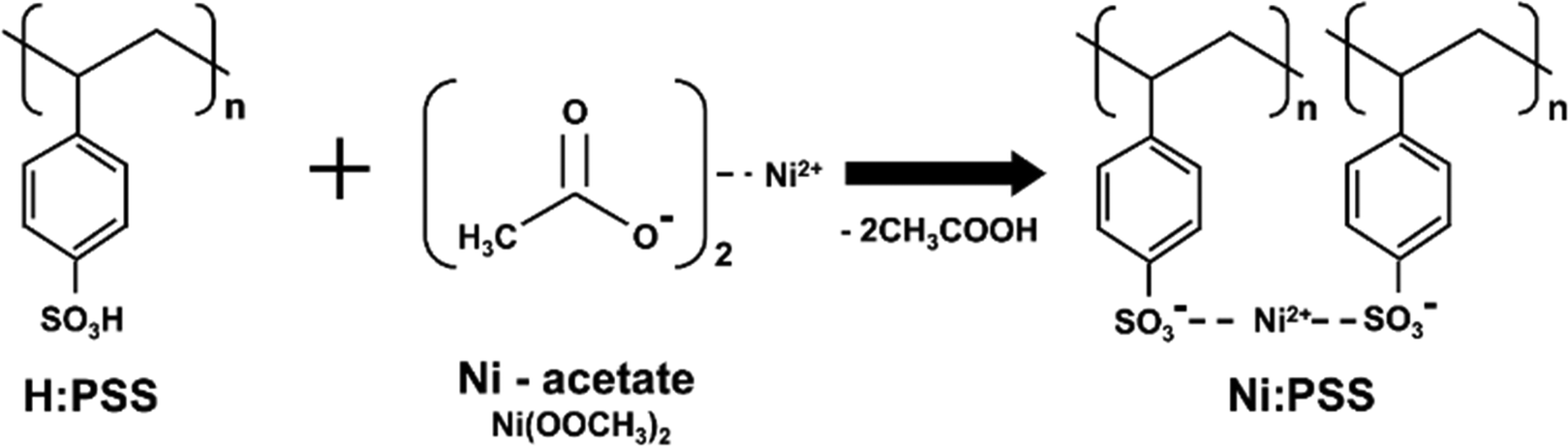 | ||
| Scheme 1 The synthesis of Ni:PSS from poly(4-styrene sulfonic acid) and Ni-acetate. | ||
We evaluated the photovoltaic properties of PeSCs made with the inverted device architectures (Fig. 1a). Current density–voltage (J–V) curves for the PeSC device are shown in Fig. 1b, and the associated solar cell parameters are reported in Table 1 (additional detailed information are included in the ESI,† Fig. S1, S2 and Table S2). Experiments were conducted to optimize the Ni:PSS thickness for each condition, and PEDOT:PSS was blended with the optimized Ni:PSS. Ni:PSS was applied as a thin interlayer (like LiF) with an optimized thickness of 0.83 nm for PeSCs and 1.79 nm for OSCs. UV-vis spectra showed that, although the layers were thin, they did result in films on ITO with small but significant absorption in the UV range (Fig. S3, ESI†) as the thickness decreased to 0.83 nm. The presence of Ni:PSS on the substrate surface was also confirmed by the Ni2+ signal in XPS, as discussed later. Specifically, for the PeSC, 10 μl, 30 μl, 50 μl, and 70 μl of PEDOT:PSS were added to 1 mL of 0.01 wt% Ni:PSS solution to optimize the Ni:PEDOT:PSS film composition. For the organic solar cell, the Ni:PEDOT:PSS film was optimized by adding 10 μl, 40 μl, 70 μl, 130 μl, 200 μl, and 400 μl of PEDOT:PSS to 1 mL of 0.05 wt% Ni:PSS solution. For the perovskite device with the Ni:PSS interlayer, device characteristics include an open circuit voltage (VOC) = 0.95 V, short circuit current density (JSC) = 17.83 mA cm−2, fill factor (FF) = 54.49%, and PCE = 9.41%. In contrast, the benchmark PEDOT:PSS HTL-based device shows relatively higher efficiency (VOC = 0.85 V, JSC = 19.09 mA cm−2, FF = 76.97% and PCE = 14.02%). Kang and coworkers developed an improved layer when a copper polyelectrolyte and PEDOT:PSS were mixed and used as an HTL between the active layer and the electrode, which showed improved characteristics compared to either material alone,36 a result of reduced recombination loss and improved carrier extraction efficiency. To enhance the hole extraction ability of Ni:PSS, PEDOT:PSS was used in small quantities as an additive with Ni:PSS. Mixed Ni:PEDOT:PSS resulted in 15.67% PCE, which was higher than either single Ni:PSS or PEDOT:PSS alone; a histogram of device performance is included in the ESI† (Fig. S2). The relatively low FF can be explained by recombination losses and ineffective carrier extraction when neat Ni:PSS is used. In this work, we can also attribute low FF to recombination that takes place at the anode due to the inability of ultra-thin layers of Ni:PSS to prevent the reverse diffusion of electrons toward ITO.41 PEDOT:PSS effectively suppresses reverse diffusion because it is relatively thick and has a high concentration of p-type charge carriers, while Ni:PSS thin films alone allow reverse diffusion through quantum tunneling of electrons, especially when the electric field is weak (near the VOC), leading to increased recombination and manifesting as a low FF.
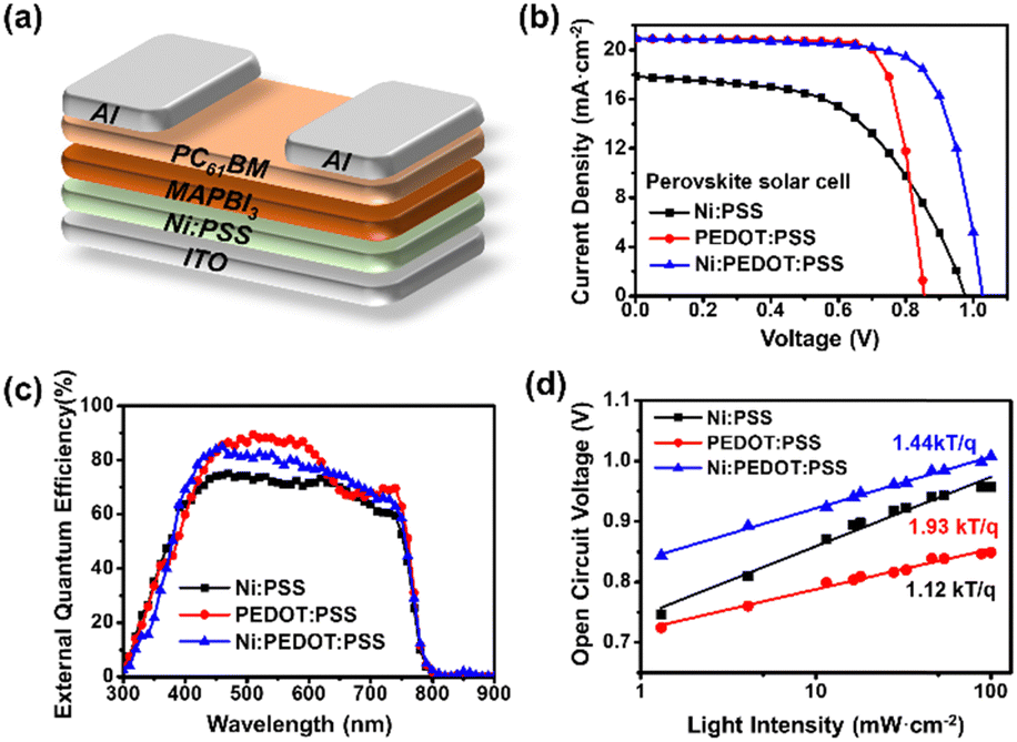 | ||
| Fig. 1 (a) Device structure of p-i-n perovskite solar cells, (b) J–V characteristics, (c) external quantum efficiency spectra, and (d) light dependence of perovskite solar cells with Ni:PSS, PEDOT:PSS and PEDOT:PSS-doped Ni:PSS HTLs. | ||
| HTLs | Thickness (nm) | JSC (mA cm−2) | JSC-EQE (mA cm−2) | VOC (V) | FF (%) | PCE (%) | |
|---|---|---|---|---|---|---|---|
| Best | Average | ||||||
| Ni:PSS | 0.83 | 17.83 ± 0.74 | 16.90 | 0.95 ± 0.04 | 54.49 ± 4.10 | 9.41 | 9.28 ± 0.25 |
| PEDOT:PSS | 25.06 | 19.09 ± 1.15 | 18.92 | 0.85 ± 0.01 | 76.97 ± 3.20 | 14.02 | 12.48 ± 0.89 |
| Ni:PEDOT:PSS | 5.33 | 19.12 ± 0.97 | 18.46 | 1.01 ± 0.01 | 71.79 ± 4.30 | 15.67 | 13.79 ± 0.67 |
Because Ni:PSS solutions are very dilute, the observed differences in performance between PEDOT:PSS and mixed Ni:PEDOT:PSS might be attributed to the greater dilution of the mixed solution, or due to the decreased thickness of the mixed HTL, rather than the presence of Ni:PSS. To investigate this possibility, pristine PEDOT:PSS solutions were diluted with an equal volume of deionized water compared to the volume of Ni:PSS solution used to make mixed Ni:PEDOT:PSS films. Device data corresponding to this experiment are shown in Fig. S4 and Table S3 (ESI†). In the case of the material containing Ni:PSS, a significantly higher VOC was observed, whereas the dilute PEDOT:PSS HTL yielded the same VOC observed for the thick PEDOT:PSS HTL, confirming that the presence of Ni affects the device characteristics.
EQE plots (Fig. 1c) show similar spectral response for devices with all three HTLs, since they all contain the same perovskite active layer. However, a few small but significant differences in the spectral shape can be attributed to the following effects. The PEDOT:PSS device shows relatively lower photocurrent efficiency in the in the near-infrared (NIR) region, which can be attributed to the parasitic absorption of PEDOT:PSS which increases in the NIR.31,42 The lower overall current of pure Ni:PSS can be attributed to the higher series resistance of this device, which is apparent as a low slope in the J–V curve near the VOC compared to other devices. The integrated current densities of the EQE spectra for Ni:PSS, PEDOT:PSS, and Ni:PEDOT:PSS PeSCs are 16.90 mA cm−2, 18.92 mA cm−2, and 18.46 mA cm−2, respectively, which are in good agreement with the JSC calculated from the J–V characteristic curves (Fig. 1c).
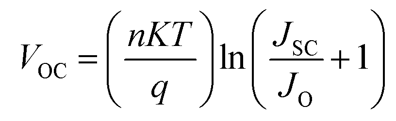
In order to understand recombination losses more thoroughly, variable light intensity experiments were conducted. Fig. 1d shows the VOC as a function of illumination intensity, fit with the equation:43,44
 | (1) |
The morphology of the HTL and ETL between the electrode and the active layer has a substantial impact on the device's overall performance, and the morphology was studied using AFM. Topographic images of Ni:PSS films on ITO substrates are shown in Fig. S5 (ESI†) under various processing conditions. Fig. S5 (a)–(e) (ESI†) show the morphology of Ni:PSS at various thicknesses, and Fig. S5 (f)–(j) (ESI†) shows the morphology of Ni:PEDOT:PSS. Fig. S5 (e)–(j) (ESI†) show champion devices for Ni:PSS and PEDOT:PSS, respectively. The roughness of all the Ni:PSS films decreased compared to ITO (RMS = 1.74 nm), which is desirable for subsequent coating of the active layer and is consistent with the deposition of a thin polymer layer on top of the ITO substrates.
It is well known that perovskite film crystallinity and morphology play an essential role in the performance of PeSCs. Therefore, scanning electron microscopy (SEM) was used to analyze the morphology of the CH3NH3PbI3 films grown on different HTLs. SEM images of perovskite films deposited onto HTL surfaces coated under various conditions are shown in Fig. S6 (ESI†). Fig. S6 (a)–(e) (ESI†) show SEM images of Ni:PSS at various thicknesses, and Fig. S6 (f)–(J) (ESI†) show SEM images of Ni:PSS doped with PEDOT:PSS. Grain sizes corresponding to the images in Fig. S6 (ESI†) were calculated using ImageJ software, as summarized in Table S2 (ESI†). SEM images of perovskite films grown on Ni:PSS are nearly identical to those coated on ITO, but with increased grain size and agglomerated tiny particles. Pinholes and small particles, as seen in films deposited on bare ITO and Ni:PSS, have the potential to increase recombination in completed devices, which has a detrimental effect on performance. Because of the very low thickness of single Ni:PSS layers, these films may not completely cover the substrate, and thus are expected to have a lower FF value and relatively low performance due to many pinholes and traps. In contrast, the larger grain size of Ni:PSS led to an improvement in VOC. Numerous papers have correlated large grain size with increased device parameters and the effectiveness of photocurrent extraction.50,51 That is, the use of Ni:PSS and Ni:PEDOT:PSS resulted in a larger average grain size of the perovskite layer, leading to an improvement in VOC (Table S4, ESI†). In particular, Ni:PEDOT:PSS enhanced the FF value by reducing pinholes and further improved VOC by increasing the particle size, resulting in a higher PCE than PEDOT:PSS. Also, to clarify the influence of the HTLs on film crystallinity, X-ray diffraction (XRD) patterns were collected to analyse the crystal structure of the perovskite films. The XRD data of the perovskite films on Ni:PSS surfaces with variable treatment conditions including (a) concentration of Ni:PSS and (b) Ni:PEDOT:PSS are shown in the (Fig. S7, ESI†). The perovskite films showed no significant change in the tetragonal structure of MAPbI3, consistently exhibiting the same features corresponding to the (110) and (220) diffraction planes. The Scherrer equation, L = Kλ/βcosθ, relates the average size of small crystal domains (L) to the XRD radiation of wavelength λ (nm) via the full width at half maximum of the peaks (β) in the intensity vs. 2θ pattern. Scherrer's equation was used to further evaluate the crystallite size of the perovskite films on each HTL. These data are summarized in the ESI† (Table S4). Because perovskite film thicknesses are very small compared to the domain sizes observed in SEM, and because they are polycrystalline, crystallite sizes calculated by the Scherrer equation are typically much smaller than domain sizes observed by SEM. Although all of the calculated crystallite sizes were in the range of 46–58 Å, the crystallite sizes were consistently larger on Ni:PSS and Ni:PEDOT:PSS films than PEDOT:PSS itself.
In addition to perovskite active layers, we investigated the use of Ni:PSS with PEDOT:PSS as HTLs with organic active layers. We performed device optimization for OSCs based on PM6:Y6; the device architectures of the Ni:PSS layer and the traditional BHJ are shown in Fig. 2a. Fig. 2b shows the J–V characteristics of the OSCs based on PM6:Y6, and Fig. 2c shows the EQE responses of the corresponding devices. The photovoltaic parameters are summarized in Table 2 for comparison (a complete set of device characteristics are included in the ESI,† Fig. S8 and Table S3). The device with Ni:PSS exhibited a PCE of 12.10%, with a JSC of 25.95 mA cm−2, a VOC of 0.68 V, and a FF of 64.60%. Compared to the device using PEDOT:PSS, the PCE was lower due to lower VOC and FF values. After blending PEDOT:PSS, all parameters, including JSC, VOC, and FF, increased, leading to a PCE of 16.50% (Ni:PEDOT:PSS). We anticipated that using an HTL with pH close to neutral would increase stability by preventing substrate corrosion. However, devices using single Ni:PSS exhibited low stability despite its neutral pH. Although the neutral pH may decrease substrate corrosion, it is apparent that other issues, such as structural defects such and reverse diffusion of holes thru the thin HTL, limit the stability of these devices. On the other hand, Ni:PEDOT:PSS, which is less acidic than PEDOT:PSS, showed better stability than PEDOT:PSS, while being able to blocking back diffusion of carriers due to its appropriate thickness (Fig. S8 (b), ESI†).
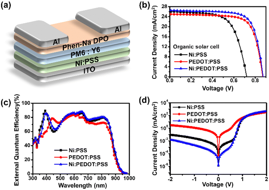 | ||
| Fig. 2 (a) Device structure of PM6:Y6 solar cells. (b) J–V characteristics, (c) external quantum efficiency characteristics, and (d) dark J–V characteristics of PM6:Y6 solar cells with Ni:PSS, PEDOT:PSS and Ni:PEDOT:PSS HTLs. | ||
| HTLs | Thickness (nm) | JSC (mA cm−2) | JSC-EQE (mA cm−2) | VOC (V) | FF (%) | PCE (%) | |
|---|---|---|---|---|---|---|---|
| Best | Average | ||||||
| Ni:PSS | 1.79 | 25.95 ± 0.36 | 25.35 | 0.68 ± 0.03 | 64.60 ± 1.40 | 12.10 | 11.20 ± 0.65 |
| PEDOT:PSS | 25.06 | 25.37 ± 0.23 | 24.35 | 0.86 ± 0.01 | 72.70 ± 1.00 | 15.80 | 15.60 ± 0.12 |
| Ni:PEDOT:PSS | 15.23 | 26.56 ± 0.31 | 25.98 | 0.87 ± 0.01 | 71.80 ± 1.40 | 16.90 | 16.50 ± 0.25 |
We observed an increase in EQE over most of the visible spectrum (350–900 nm) for Ni:PSS and Ni:PEDOT:PSS devices compared to PEDOT:PSS devices. Ni:PSS Devices consistently exhibited enhanced photocurrent generation at 350–400 nm compared with the PEDOT:PSS devices, which can be attributed to an optical interference effect, while the increase in the NIR part of the spectrum can be attributed reduced parasitic absorption of PEDOT. Utilizing Ni:PSS, PEDOT:PSS, and PEDOT:Ni:PSS had integrated current densities of 25.35, 24.35, and 25.98 mA cm−2, respectively. Using Ni:PSS, PM6:Y6 OSCs had significantly increased optical field intensity in the active layer at wavelengths near the absorption onset. Since Ni:PSS is about 25 nm thinner than PEDOT:PSS, the optical field distribution of the active layer is changed, resulting in increased absorption in the lower wavelength range (350–400 nm) as well as stronger photocurrent generation in the NIR, where the parasitic absorption of PEDOT:PSS is higher. The increased field strength resulted in increased charge carrier generation rate in these wavelength ranges and a higher device JSC. As a result, when Ni:PSS is used instead of PEDOT:PSS, the JSC increases, and the increased value was maintained upon adding a small amount of PEDOT:PSS.
We characterized the series resistance and shunt resistance from dark J–V data to better understand the effect of Ni:PSS on the characteristics of OSCs (Fig. 2d). Analyzing the shunt resistance (RSh) and series resistance (RS) of devices with diffferent HTLs helps to better understand the JSC and FF results (Fig. S8 (c), ESI†). Table S6 (ESI†) summarizes the detailed parameters. Shunt and series resistance determine the capability of JSC and FF,52 and high shunt and low series resistance result in higher device performance under illumination. The device with a single Ni:PSS layer exhibited a low shunt resistance of 1.047 KΩ cm2, which can be attributed to photocarrier losses caused by leakage through the ultra-thin HTL. The series resistance reduced from 0.187 Ω cm2 (PEDOT:PSS) to 0.142 Ω cm2 (Ni:PEDOT:PSS) as the doped PEDOT:PSS increased, but the shunt resistance grew from 63.613 KΩ cm2 (PEDOT:PSS) to 1074.440 KΩ cm2 (Ni:PEDOT:PSS), indicating improved diode characteristics in this HTL. High shunt and low series resistance in devices led to improved performance due to reduced current leakage and optical carrier losses.53
Finally, photoelectron spectroscopy was used to create band diagrams to understand the charge carrier dynamics in the devices. Detailed UPS data for all conditions is included in Fig. S9–S17 and Tables S7–S8 (ESI†) of the while Fig. 3 summarizes the thickness-dependent energy band structure of the active material inside the device. Relevant information obtained from XPS includes film thickness. If the film is less thick than the sampling depth of the optoelectronics and the spectral attenuation between the film and the substrate can determine the film thickness. By modifying the Beer–Lambert law, precise measurements can be made based on the attenuated spectrum. The thickness of each deposited layer is d.
 | (2) |
![[double bond, length as m-dash]](https://www.rsc.org/images/entities/char_e001.gif) O bonding appeared in the S 2p and O 1s spectra, respectively, with increasing Ni:PSS film thickness.
O bonding appeared in the S 2p and O 1s spectra, respectively, with increasing Ni:PSS film thickness.
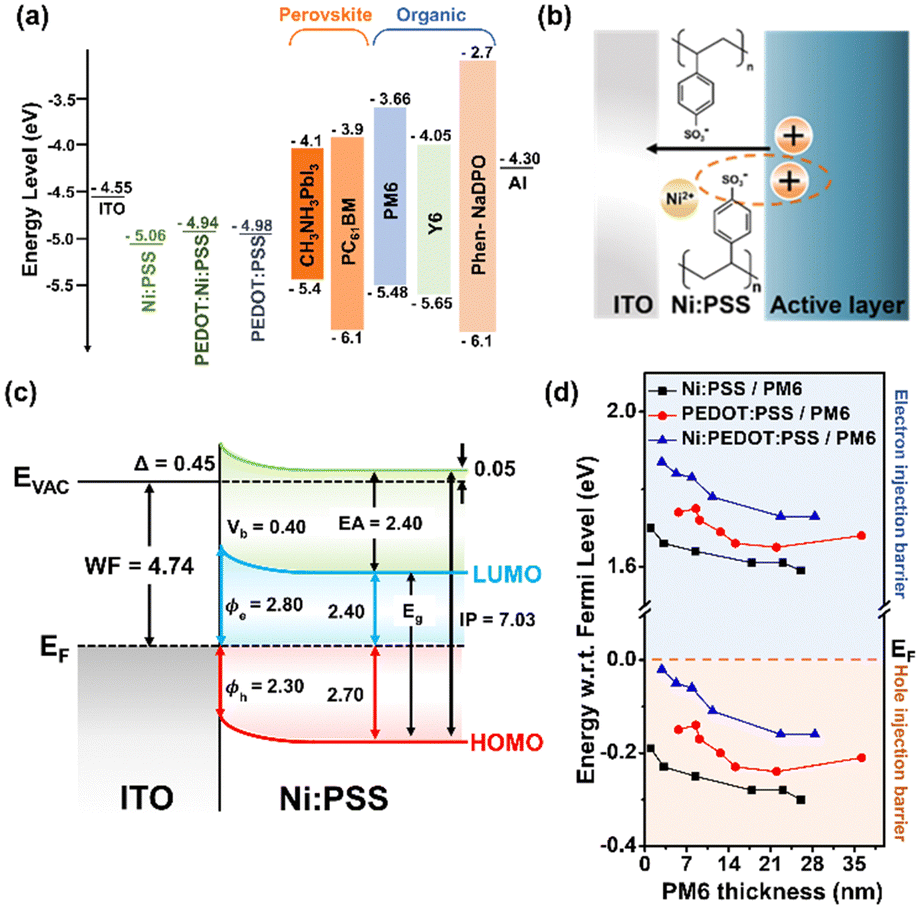 | ||
| Fig. 3 (a) Energy level diagram of the studied devices, (b) the interaction between the anionic sulfonate moieties and holes in the Ni:PSS/active layer, (c) energy level diagram of ITO/Ni:PSS, and (d) band bending diagram based on observed changes in WF, IP, and EA of PM6 deposted on ITO/Ni:PSS. | ||
UPS was used to analyze the electronic band structure at the anode interface. A schematic diagram showing the mechanism by which Ni:PSS is able to influence the band structure at the BHJ interface as a polyelectrolyte is shown in Fig. 3b. Ni2+ can accept electrons in reversible redox reactions, forming Ni+ or Ni0. When Ni2+ accepts electrons in the active layer, it leads to a decrease in electrons at the interface between the HTL and the active layer. This, in turn, increases hole concentration due to the enhanced positive charge, facilitating hole extraction and flow towards the electrode. Ni:PEDOT:PSS further improves hole extraction and flow by enhancing the extraction ability.
Combining XPS and UPS data yields an ITO/Ni:PSS interface energy level diagram, as shown in Fig. 3c, where EVAC denotes the vacuum level, EF the Fermi level, EA the electron affinity, IP the ionization potential, Eg the band gap energy, ϕ the WF, ϕe the electron injection barrier, ϕh the hole injection barrier, and Δ is the interface dipole. Using a UPS and a HeI light source, the HTLs of three sample HTLs were measured. The WF values for Ni:PSS, PEDOT:PSS, and Ni:PEDOT:PSS were found to be −5.06, −4.98, and −4.94 eV using the equation ϕ = hv + ESE, where hv = 21.22 eV is the incident photon energy from the HeI+ source. For information on band banding, the shifts of the C 1s and S 2p peaks are shown in Fig. S11–S14 (ESI†), where the positions are plotted against the layer thickness. The peak shift for the initial (thinnest) Ni:PSS monolayer was computed. Ni:PSS displayed a 0.40 eV low binding energy shift as thickness increased. The S 2p peak and the C 1s peak exhibit a similar tendency. Ni:PSS thin films composed of nickel cations and PSS anions, form interfacial dipoles on the ITO surface, leading to a slight improvement in the effective WF of the substrate. Increasing the WF of ITO can result in ohmic contact with the p-type semiconductor or perovskites. In turn, able to increase the VOC and reduce carrier recombination in perovskite devices, leading to improved performance.
Characterizing interfacial contacts and quantifying energy barriers between interfaces is essential for understanding and improving device efficiency. Changes in the barrier for PM6 films of various thicknesses are shown in Fig. 3d. When the EF of two different substances differ, electrons move from the material with higher EF to the material with lower EF until equilibrium is attained. At the interface between the HTL and PM6, the equilibration of the EF leads to a change in the HOMO band. The change in the EF is found to be 0.19 eV for thin films and 0.30 eV for thick films at the Ni:PSS/PM6 interface. This transformation of the energy band enables efficient hole transfer at the Ni:PSS and PM6 interface. In other words, Ni:PSS is p-doped with nickel and has an excellent ability to extract holes from PM6 and form an ohmic contact. Similar observations are made at the PEDOT:PSS/PM6 interface, where the EF change increases from 0.15 eV (thin thickness) to 0.21 eV (thick thickness). The overall device parameters are positively affected by the lower ϕh values than single Ni:PSS devices. At the Ni:PEDOT:PSS/PM6 interface, the EF changes from 0.02 eV (thin thickness) to 0.16 eV (thick thickness), which has a very small value when the thickness is thin. This change in EF enhances the ability to extract holes, making it possible to achieve better OSCs by adding a small amount of PEDOT:PSS. Blending PEDOT:PSS into a single Ni:PSS layer creates a p-type band bending effect, reducing the hole extraction barrier, and increasing the electron barrier, thereby suppressing recombination while creating an ohmic contact.
4. Conclusions
In conclusion, we’ve investigated the use of a new HTL incorporating an organic polymer (PSS) and an ionized metal (nickel) in both PeSCs and OSCs. We’ve explored several approaches to its application using it alone as an HTL and by blending with PEDOT:PSS. It functions modestly as an HTL by itself, however, we demonstrate an efficiency enhancement relative to PEDOT:PSS when mixed HTLs are used. UPS and XPS measurements provide a detailed understanding of the interfacial energy level alignment, electronic band structure, and band bending at the HTL/PM6 interface. In perovskite and organic solar cells, the single Ni:PSS layer by itself resulted in modest efficiencies of 9.41% and 12.10%, respectively. The use of Ni:PSS provided the advantages of high VOC for PeSCs and high JSC for OSCs. For both devices, the use of Ni:PSS alone had relatively low efficiency due to a low FF, however, a beneficial effect when mixed with PEDOT:PSS. By blending with PEDOT:PSS, the FF could be improved resulting in increased PCEs of up to 15.67% (PeSC) and 16.60% (OSC) when PEDOT:PSS and Ni:PSS were combined. In PeSCs, only the VOC improved due to the increased built-in potential of the perovskite layer caused by the elevated WF of the substrate. In contrast, OSCs, which had the same built-in potential (determined by PM6:Y6), resulted in no change in VOC. However, the thin Ni:PSS layers in OSCs increased current density due to the reduced parasitic absorption and intensified incident light. However, XPS and UPS data confirmed that a single Ni:PSS layer alone has poor hole extraction ability because it cannot prevent back diffusion of electrons and leads to high recombination rates. Due to the changed Fermi level, quick extraction of holes and electrons based on Ohmic contacts decreased leakage current and carrier recombination, and blending PEDOT:PSS increased efficiency. This study provides insights into the role of nickel ions and anionic polyelectrolytes on the energy band structure and performance of both perovskite and organic solar cells, helping to expand the knowledge of the effects of ions on anode interfaces and helping to design better HTLs in the future.Conflicts of interest
There are no conflicts to declare.Acknowledgements
This work was supported by the 2022 Research Fund of the University of Seoul.References
- S. Lu, C. Chen and J. Tang, Front. Optoelectron., 2020, 13, 246–255 CrossRef PubMed.
- T. G. Allen, J. Bullock, X. Yang, A. Javey and S. De Wolf, Nat. Energy, 2019, 4, 914–928 CrossRef CAS.
- S. Essig, C. Allebé, T. Remo, J. F. Geisz, M. A. Steiner, K. Horowitz, L. Barraud, J. S. Ward, M. Schnabel, A. Descoeudres, D. L. Young, M. Woodhouse, M. Despeisse, C. Ballif and A. Tamboli, Nat. Energy, 2017, 2, 17144 CrossRef CAS.
- P. Cheng and X. Zhan, Chem. Soc. Rev., 2016, 45, 2544–2582 RSC.
- M. Kaltenbrunner, M. S. White, E. D. Głowacki, T. Sekitani, T. Someya, N. S. Sariciftci and S. Bauer, Nat. Commun., 2012, 3, 770 CrossRef PubMed.
- M. A. Alkhalayfeh, A. A. Aziz and M. Z. Pakhuruddin, Renewable Sustainable Energy Rev., 2021, 141, 110726 CrossRef CAS.
- Y. Miyake and A. Saeki, J. Phys. Chem. Lett., 2021, 12, 12391–12401 CrossRef CAS PubMed.
- W. Gao, F. Qi, Z. Peng, F. R. Lin, K. Jiang, C. Zhong, W. Kaminsky, Z. Guan, C. S. Lee, T. J. Marks, H. Ade and A. K. Y. Jen, Adv. Mater., 2022, 34, 1–11 Search PubMed.
- Y. Wei, Z. Chen, G. Lu, N. Yu, C. Li, J. Gao, X. Gu, X. Hao, G. Lu, Z. Tang, J. Zhang, Z. Wei, X. Zhang and H. Huang, Adv. Mater., 2022, 34, 1–8 Search PubMed.
- M. T. Dang, L. Hirsch and G. Wantz, Adv. Mater., 2011, 23, 3597–3602 CrossRef CAS PubMed.
- S. H. Liao, H. J. Jhuo, Y. S. Cheng and S. A. Chen, Adv. Mater., 2013, 25, 4766–4771 CrossRef CAS PubMed.
- J. Yuan, Y. Zhang, L. Zhou, G. Zhang, H. L. Yip, T. K. Lau, X. Lu, C. Zhu, H. Peng, P. A. Johnson, M. Leclerc, Y. Cao, J. Ulanski, Y. Li and Y. Zou, Joule, 2019, 3, 1140–1151 CrossRef CAS.
- M. Zhang, X. Guo, W. Ma, H. Ade and J. Hou, Adv. Mater., 2015, 27, 4655–4660 CrossRef CAS PubMed.
- X. Gong, M. Tong, Y. Xia, W. Cai, J. S. Moon, Y. Cao, G. Yu, C. L. Shieh, B. Nilsson and A. J. Heeger, Science, 2009, 325, 1665–1667 CrossRef CAS PubMed.
- Y. Liang, Y. Wu, D. Feng, S. T. Tsai, H. J. Son, G. Li and L. Yu, J. Am. Chem. Soc., 2009, 131, 56–57 CrossRef CAS PubMed.
- W. Zhu, A. P. Spencer, S. Mukherjee, J. M. Alzola, V. K. Sangwan, S. H. Amsterdam, S. M. Swick, L. O. Jones, M. C. Heiber, A. A. Herzing, G. Li, C. L. Stern, D. M. DeLongchamp, K. L. Kohlstedt, M. C. Hersam, G. C. Schatz, M. R. Wasielewski, L. X. Chen, A. Facchetti and T. J. Marks, J. Am. Chem. Soc., 2020, 142, 14532–14547 CrossRef CAS PubMed.
- A. Kojima, K. Teshima, Y. Shirai and T. Miyasaka, J. Am. Chem. Soc., 2009, 131, 6050–6051 CrossRef CAS PubMed.
- M. A. Green, A. Ho-Baillie and H. J. Snaith, Nat. Photonics, 2014, 8, 506–514 CrossRef CAS.
- W. Shockley and H. J. Queisser, J. Appl. Phys., 1961, 32, 510–519 CrossRef CAS.
- Z. Yang, B. H. Babu, S. Wu, T. Liu, S. Fang, Z. Xiong, L. Han and W. Chen, Sol. RRL, 2020, 4, 1–16 CAS.
- Y. Hou, X. Du, S. Scheiner, D. P. McMeekin, Z. Wang, N. Li, M. S. Killian, H. Chen, M. Richter, I. Levchuk, N. Schrenker, E. Spiecker, T. Stubhan, N. A. Luechinger, A. Hirsch, P. Schmuki, H. P. Steinrück, R. H. Fink, M. Halik, H. J. Snaith and C. J. Brabec, Science, 2017, 358, 1192–1197 CrossRef CAS PubMed.
- J. H. Seo, A. Gutacker, Y. Sun, H. Wu, F. Huang, Y. Cao, U. Scherf, A. J. Heeger and G. C. Bazan, J. Am. Chem. Soc., 2011, 133, 8416–8419 CrossRef CAS PubMed.
- K. Yuan, L. Chen and Y. Chen, J. Phys. Chem. B, 2014, 118, 11563–11572 CrossRef CAS PubMed.
- G. E. Lim, Y. E. Ha, M. Y. Jo, J. Park, Y. C. Kang and J. H. Kim, ACS Appl. Mater. Interfaces, 2013, 5, 6508–6513 CrossRef CAS PubMed.
- B. Walker, H. Choi and J. Y. Kim, Curr. Appl. Phys., 2017, 17, 370–391 CrossRef.
- A. Guerrero, S. Chambon, L. Hirsch and G. Garcia-Belmonte, Adv. Funct. Mater., 2014, 24, 6234–6240 CrossRef CAS.
- Q. D. Yang, J. Li, Y. Cheng, H. W. Li, Z. Guan, B. Yu and S. W. Tsang, J. Mater. Chem. A, 2017, 5, 9852–9858 RSC.
- Y. Meng, Z. Hu, N. Ai, Z. Jiang, J. Wang, J. Peng and Y. Cao, ACS Appl. Mater. Interfaces, 2014, 6, 5122–5129 CrossRef CAS PubMed.
- J. J. Lee, S. H. Lee, F. S. Kim, H. H. Choi and J. H. Kim, Org. Electron., 2015, 26, 191–199 CrossRef CAS.
- J. Lee, H. Kang, S. Kee, S. H. Lee, S. Y. Jeong, G. Kim, J. Kim, S. Hong, H. Back and K. Lee, ACS Appl. Mater. Interfaces, 2016, 8, 6144–6151 CrossRef CAS PubMed.
- J. Cameron and P. J. Skabara, Mater. Horiz., 2020, 7, 1759–1772 RSC.
- Y. Sun, C. J. Takacs, S. R. Cowan, J. H. Seo, X. Gong, A. Roy and A. J. Heeger, Adv. Mater., 2011, 23, 2226–2230 CrossRef CAS PubMed.
- C. Zuo and L. Ding, Small, 2015, 11, 5528–5532 CrossRef CAS PubMed.
- W. Chen, F. Z. Liu, X. Y. Feng, A. B. Djurišić, W. K. Chan and Z. B. He, Adv. Energy Mater., 2017, 7, 1–8 Search PubMed.
- W. Chen, Y. Wu, Y. Yue, J. Liu, W. Zhang, X. Yang, H. Chen, E. Bi, I. Ashraful, M. Grätzel and L. Han, Science, 2015, 350, 944–948 CrossRef CAS PubMed.
- F. Shoukat, J. H. Kang, Y. Khan, Y. J. Park, J. H. Lee, B. Walker and J. H. Seo, Adv. Mater. Interfaces, 2023, 10, 2300043 CrossRef CAS.
- J. H. Lee, Y. Khan, S. Kim, A. J. Choi, B. Walker, S. Park and J. H. Seo, Adv. Funct. Mater., 2024, 2315074 CrossRef.
- J. H. Kang, A. K. Harit, J. E. Jeong, H. Y. Woo, J. H. Seo and B. Walker, Sol. RRL, 2021, 5, 2100521 CrossRef CAS.
- Y. Sun, S. C. Chien, H. L. Yip, Y. Zhang, K. S. Chen, D. F. Zeigler, F. C. Chen, B. Lin and A. K. Y. Jen, Chem. Mater., 2011, 23, 5006–5015 CrossRef CAS.
- Y. Yang, Q. Kang, Q. Liao, Z. Zheng, C. He, B. Xu and J. Hou, ACS Appl. Mater. Interfaces, 2020, 12, 39462–39470 CrossRef CAS PubMed.
- A. Ali, Y. Ahn, K. A. Khawaja, J. H. Kang, Y. J. Park, J. H. Seo and B. Walker, Adv. Funct. Mater., 2021, 31, 1–10 Search PubMed.
- B. J. Bruijnaers, E. Schiepers, C. H. L. Weijtens, S. C. J. Meskers, M. M. Wienk and R. A. J. Janssen, J. Mater. Chem. A, 2018, 6, 6882–6890 RSC.
- A. K. K. Kyaw, D. H. Wang, V. Gupta, W. L. Leong, L. Ke, G. C. Bazan and A. J. Heeger, ACS Nano, 2013, 4569–4577 CrossRef CAS PubMed.
- T. Singh and T. Miyasaka, Adv. Energy Mater., 2018, 8, 1700677 CrossRef.
- Z. Li, W. Wang, N. C. Greenham and C. R. McNeill, Phys. Chem. Chem. Phys., 2014, 16, 25684–25693 RSC.
- G. A. H. Wetzelaer, M. Kuik, M. Lenes and P. W. M. Blom, Appl. Phys. Lett., 2011, 99, 153506 CrossRef.
- D. Zhao, M. Sexton, H. Y. Park, G. Baure, J. C. Nino and F. So, Adv. Energy Mater., 2015, 5, 1–5 Search PubMed.
- S. Shao, Z. Chen, H. H. Fang, G. H. Ten Brink, D. Bartesaghi, S. Adjokatse, L. J. A. Koster, B. J. Kooi, A. Facchetti and M. A. Loi, J. Mater. Chem. A, 2016, 4, 2419–2426 RSC.
- K. Abiedh, Z. Zaaboub and F. Hassen, Appl. Phys. A: Mater. Sci. Process., 2021, 127, 1–9 CrossRef.
- A. Al Mamun, T. T. Ava, H. J. Jeong, M. S. Jeong and G. Namkoong, Phys. Chem. Chem. Phys., 2017, 19, 9143–9148 RSC.
- H. Nazem, H. P. Dizaj and N. E. Gorji, Superlattices Microstruct., 2019, 128, 421–427 CrossRef CAS.
- D. I. Kim, J. W. Lee, R. H. Jeong and J. H. Boo, Sci. Rep., 2022, 12, 1–10 CrossRef PubMed.
- B. H. Lee, I. H. Jung, H. Y. Woo, H. K. Shim, G. Kim and K. Lee, Adv. Funct. Mater., 2014, 24, 1100–1108 CrossRef CAS.
Footnote |
| † Electronic supplementary information (ESI) available. See DOI: https://doi.org/10.1039/d4ya00081a |
| This journal is © The Royal Society of Chemistry 2024 |