Commercially available InSb as a high-performance anode for secondary batteries towards superior lithium storage†
Wenying
Li‡
a,
Tingting
Liu‡
a,
Jundong
Zhang‡
a,
Na
Peng
a,
Runtian
Zheng
a,
Haoxiang
Yu
a,
Ying
Bai
 *b,
Yanhua
Cui
 *c and
Jie
Shu
 *a
*a
aFaculty of Materials Science and Chemical Engineering, Ningbo University, Ningbo 315211, Zhejiang, China. E-mail: shujie@nbu.edu.cn
bHenan Key Laboratory of Photovoltaic Materials and School of Physics & Electronics, Henan University, Kaifeng 475004, Henan, China. E-mail: ybai@henu.edu.cn
cInstitute of Electronic Engineering, China Academy of Engineering Physics, Mianyang 621000, Sichuan, China. E-mail: cuiyanhua@netease.com
First published on 26th July 2019
Abstract
Alloying lithiation hosts have aroused much more interest due to their remarkable volumetric/gravimetric capacity. Among them, Sb-based binary or ternary alloys have become an appealing anode candidate owing to their good electronic conductivity. In this work, commercially available InSb is employed as an anode host material due to its excellent electrochemical capability proved via various electrochemical tests. InSb exhibits an initial specific charge capacity of 680.9 mA h g−1. Meanwhile, 78.6% of the initial charge capacity can be retained after the 80th cycle. By in situ X-ray diffraction (XRD), ex situ scanning electron microscopy (SEM), and ex situ transmission electron microscopy (TEM), InSb displays high structural stability and electrochemical reversibility. All these advantages suggest that InSb alloys as anode materials have great potential applications in the future.
1. Introduction
In the last few decades, fossil fuels have been consumed very rapidly, which causes a lot of problems such as environmental pollution, energy crises, greenhouse effects and ecological imbalances. Therefore, the development of renewable energy sources has become crucial. Among them, lithium-ion battery (LIB) technology has played a pivotal role due to its wide application in many fields, such as grid storage, portable electronics and electric vehicles.1–4 In commercial LIBs, graphite is extensively selected as the anode electrode.5,6 However, the graphite anode can hardly fulfill the requirements of high-capability LIBs, owing to its low working voltage (0.1 V), large irreversible capacity and poor rate performance.7–12 To address these problems, considerable research studies have been conducted on transition metal oxides.13–18 The reversible capacity of transition metal oxides is approximately 2 to 3 times as high as that of graphite. However, transition metal oxides have shortcomings such as poor conductivity, rapid energy decay and volume expansion during cycling, which hinder its application in actual production.19,20 Therefore, it is worthwhile devoting much effort to finding novel anode host materials that possess high energy density, outstanding safety, and excellent cycling capability.Alloying lithiation hosts have aroused much more interest due to their remarkable gravimetric/volumetric capacity, e.g., Sn (960 mA h g−1/1991 mA h cm−3) and Ge (1384 mA h g−1/2180 mA h cm−3).21–23 However, significant volume expansion is unfavorable to the development of alloy anode materials.24–27 In order to solve this problem, many novel alloy anode materials have been studied in depth.28 Among them, Sb-based binary or ternary alloys have become an appealing anode candidate owing to their good electronic conductivity.29–34 Furthermore, it is also a conventional method to construct a Sb–M alloy by introducing a buffer matrix to improve the cycle stability of the Sb anode material. On the one hand, an active metal M is investigated to form Sb–M alloys (e.g., SnSb, Sb2Te3 and Bi–Sb alloy) as anode materials for LIBs.35–37 In comparison with pure metals, intermetallic compounds show superior cycling capabilities. The mechanical stress is reduced to a certain extent owing to the alloying/dealloying reactions of M and Sb occurring at different reaction potentials, leading to remarkable cycling/rate capabilities of the Sb–M alloys.38 On the other hand, inactive metal M can also be used to fabricate Sb–M alloys (e.g., Cu, Fe and Ni), in which the inactive metal decreases the total proportion of the active material in the electrode.39–41 Though some capacity is sacrificed, the metal M can improve the cycling/rate performance by providing structural reinforcement and electrical conductivity to the electrodes. Nevertheless, the pulverization of Sb is still caused by volume expansion, leading to the contact loss between particles in the active hosts and severe capacity decay.38 Hence, an appropriate metallic element must be selected to conceive a Sb–M alloy anode with high-performance. In this work, we find that InSb has significant electrochemical properties as an anode for LIBs. The InSb alloys can avoid the drawbacks of pure In and Sb metals through a synergistic effect.37,38
Herein, we use commercially available InSb alloy powder to carry out research. We have tested its basic electrochemical properties by cyclic voltammetry (CV) and galvanostatic discharge/charge tests. Furthermore, the lithiation/delithiation mechanism of InSb is examined using in situ and ex situ techniques, which is proved to be a typical alloying/dealloying reaction. The shortcomings of the electrochemical behavior of pure Sb and In metals can be restricted by the unique synergistic effect of the alloy anode, obtaining outstanding electrochemical performance for LIBs. According to the obtained results, InSb is a promising anode for LIBs.
2. Experimental
Commercially available InSb alloys were prepared by a solid reaction with In and Sb powders (Aladdin, 99.9%).42 Scanning electron microscopy (Hitachi S-4800) and transmission electron microscopy (JEM-2010) were performed to observe the surface morphology and particle size of InSb powders. The structural information on samples was obtained by X-ray diffraction (Bruker D8 Focus), high-resolution TEM (HRTEM) and selected-area electron diffraction (SAED). In situ structural variations of InSb were analyzed by in situ XRD in the 2θ range from 20° to 50°. The surface chemical state information on InSb was confirmed by X-ray photoelectron spectrometry (XPS, PHI-Quantum 2000).As the working electrode, InSb powder, carbon black and sodium alginate were completely ground in an agate mortar at a mass ratio of 8![[thin space (1/6-em)]](https://www.rsc.org/images/entities/char_2009.gif) :
:![[thin space (1/6-em)]](https://www.rsc.org/images/entities/char_2009.gif) 1
1![[thin space (1/6-em)]](https://www.rsc.org/images/entities/char_2009.gif) :
:![[thin space (1/6-em)]](https://www.rsc.org/images/entities/char_2009.gif) 1 to form a uniform slurry. An appropriate amount of distilled water was added and mixed well with the slurry. Shortly afterwards, the slurry was homogeneously smeared on copper foil. Then the operating films were placed and dried in a vacuum oven at 80 °C for 10 h. The detailed cell assembly and electrochemical analysis processes can be found in the ESI.†
1 to form a uniform slurry. An appropriate amount of distilled water was added and mixed well with the slurry. Shortly afterwards, the slurry was homogeneously smeared on copper foil. Then the operating films were placed and dried in a vacuum oven at 80 °C for 10 h. The detailed cell assembly and electrochemical analysis processes can be found in the ESI.†
3. Results and discussion
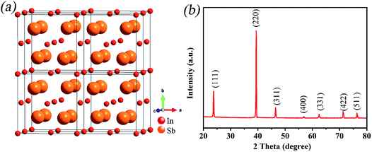
Fig. 1a depicts the complete structure model of InSb. It is obvious that InSb is a cubic phase with F![[4 with combining macron]](https://www.rsc.org/images/entities/char_0034_0304.gif) 3m space group. In addition, the lattice constants and angles agree with the following relations: a = b = c = 4.77 Å and α = β = γ = 90°. As shown in Fig. 1b, the XRD information on InSb alloy is recorded. The positions of all reflections concur with the reported data of InSb (JCPDS no. 190577), suggesting the high purity of InSb.
3m space group. In addition, the lattice constants and angles agree with the following relations: a = b = c = 4.77 Å and α = β = γ = 90°. As shown in Fig. 1b, the XRD information on InSb alloy is recorded. The positions of all reflections concur with the reported data of InSb (JCPDS no. 190577), suggesting the high purity of InSb.
The surface chemical state information on InSb is obtained by XPS analysis, and the detailed results are given in Fig. 2. Fig. 2a presents the schematic illustration of XPS. As expected, the XPS survey spectrum displays the presence of peaks corresponding to Sb 3d, In 3d and C 1s (Fig. 2b). As shown in Fig. 2c, peaks appeared at 451.8 and 444.1 eV that correspond to In 3d3/2 and In 3d5/2, respectively. Fig. 2d exhibits two peaks at 537.4 and 527.9 eV, which are well indexed to Sb 3d3/2 and Sb 3d5/2, respectively. These data are in good agreement with the findings in the literature.43–46
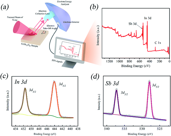 | ||
| Fig. 2 XPS spectra of InSb. (a) Schematic illustration of the observation process. (b) Survey spectrum. (c) The In 3d core-level spectrum. (d) The Sb 3d core-level spectrum. | ||
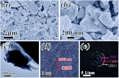
The morphology and degree of crystallization of InSb are determined by the utilization of SEM, TEM, HRTEM and SAED, and the results are provided in Fig. 3a–e. As depicted in Fig. 3a and b, it could be apparently viewed that the InSb alloy has irregular polyhedra without serious agglomeration. It is found that the particles have a size distribution ranging from 0.5 to 2 μm. Consistent with the SEM results, the TEM image in Fig. 3c shows that the morphology of InSb is an irregular polyhedron. In addition, the HRTEM image exhibits a d-spacing of 0.229 nm in Fig. 3d, attributed to the (220) crystal plane of the InSb. Fig. 3e displays the SAED pattern of InSb. From the inside out, the diffraction spots on the different rings correspond to the (111), (220) and (311) planes, which are perfectly matched with the XRD characterization results.
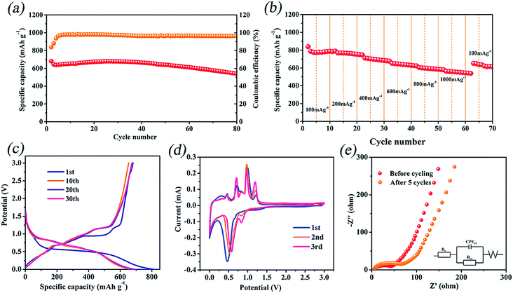
To obtain a comprehensive understanding of the electrochemical characteristics of InSb as the anode host, we have investigated the lithium storage properties of InSb. Fig. 4a displays the long-term cycling property and corresponding coulombic efficiency of InSb at 400 mA g−1. It can be seen from Fig. 4a that the coulombic efficiency of InSb is not high in the first few cycles. On the one hand, the SEI layer on the electrode surface undergoes the processes of formation, partial decomposition and re-stabilization, which leads to the low coulombic efficiency. On the other hand, the surface film formation is caused by the insertion of Li into metallic host matrices, thereby forming a new interfacial phase, which consumes a small amount of charge and makes the irreversible capacity higher.47,48 InSb shows 680.9 mA h g−1 specific charge capacity in the initial cycle. After 80 cycles, 535.5 mA h g−1 reversible capacity could still be maintained, suggesting a capacity retention of 78.6%. The initial coulombic efficiency of InSb is around 85%. In addition, the coulombic efficiency increases to approximately 100% after a few cycles and always retains this value afterwards. The result shows that the InSb is favorable for reversible lithium storage. Fig. 4b presents the rate performance of InSb with the current density increasing from 100 to 1000 mA g−1. It could be observed that the sample exhibits a stepped scattering curve. The charge capacities of InSb are 839.3, 768.6, 711.0, 652.3, 605.0 and 563.1 mA h g−1 at current densities from 100 to 1000 mA g−1. Moreover, as the current density returns to 100 mA g−1, the InSb electrode still has 652.2 mA h g−1 specific charge capacity, indicating good structural stability and high reversibility.
The 1st, 10th, 20th and 30th discharge/charge curves are also shown in Fig. 4c. It shows that the first discharge curve has a long voltage platform at about 0.44–0.58 V. Meanwhile, four charge plateaus can be observed at about 0.42–0.49 V, 0.67–0.73 V, 0.94–1.01 V, and 1.16–1.24 V, respectively. In addition, the discharge/charge curves show no significant change from the 10th cycle to the 30th cycle. The result shows that the host structure for lithium storage can be firmly maintained during long-term cycles. Fig. 4d presents the CV curves of InSb for the 1st–3rd cycles at a sweeping rate of 0.05 mV s−1 in 0–3.0 V. The reduction and oxidization peaks of CV curves are ascribed to the lithiation/delithiation, respectively. It can be observed that there are one reduction peak at voltage of 0.47 V and four oxidation peaks at 0.46, 0.72, 0.99 and 1.22 V in the first cycle, consistent with the plateaus of discharge/charge profile curves. Among them, the peak at an operating voltage of 0.47 V is owing to the formation of In and Li3Sb. In comparison to the initial sweep, the reduction peaks of the subsequent scans shift to higher operating voltage on account of the obvious decrease of cell impedance.22
The Nyquist plots of InSb cells before cycling and after 5 cycles are shown in Fig. 4e, which consist of a depressed semicircle and a sloping line. The semicircle and line correspond to the charge transfer resistance (Rct) and Warburg impedance, respectively. The inset of Fig. 4e shows the equivalent circuit model. By fitting, the charge transfer resistances of InSb before cycling and after 5 cycles are 38.85 Ω and 59.91 Ω, respectively. It can be seen that the value of resistance is not significantly increased, indicating that InSb has good electrical conductivity.
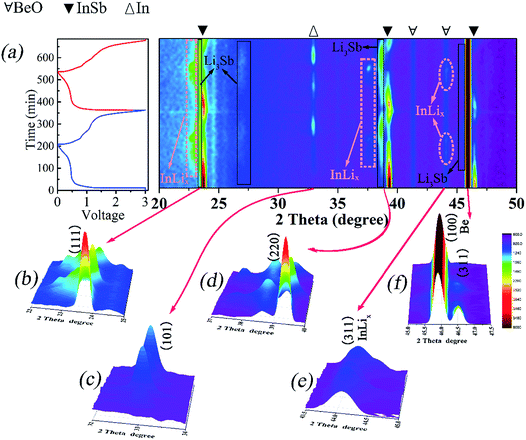
To further unveil the phase transformations in the lithiation/delithiation reactions, in situ XRD measurements are performed in the voltage range of 0–3 V in the first two cycles. As displayed in Fig. 5, in situ XRD data (2θ range of 20–50°) are collected and 75 scans are recorded. As presented in Fig. 5a, the main peaks located at 23.9°, 39.4° and 46.6°, correspond to the (111), (220) and (311) reflections of InSb. The Bragg positions at 41.4° and 44.1° belong to BeO, and the peak appearing at 45.9° is related to the Be disc.49,50 With the voltage rapidly going down from 3 to 0.7 V, the intensity of the (111), (220) and (311) peaks decreases, indicating the intercalation of lithium into InSb to form intermediate LixInSb. When the anode material is discharged to 0.47 V, two new peaks appear at 33.1° and 38.9°, corresponding to the (101) diffraction peak of In and (220) diffraction peak of Li3Sb. This suggests that a reaction of lithium with LixInSb forms metal In and a Li3Sb alloy. Meanwhile, the peaks of (111) and (220) planes for InLix are observed on account of the alloying reaction between metal In and lithium. With the continuous lithiation process, the peak intensity of InSb becomes weak whereas the peak intensity of Li3Sb becomes strong. At the final state of the initial discharge reaction, the main diffraction peaks of InSb nearly disappear. In the charge process, when the in situ cell is charged to 3 V, the main peaks of InSb re-appear with relatively weak intensity and the diffraction intensity of the (220) peak for Li3Sb becomes low. It can be inferred that the dealloying process of Li3Sb is incomplete, leading to the irreversibility of the reaction and the decay of the capacity. During the second discharge/charge process, the diffraction peaks of InSb, In, InLix and Li3Sb behave similarly to those of the first discharge/charge process.
To further obtain insights into the electrochemical-storage mechanism, ex situ TEM/HRTEM and ex situ SAED are used to monitor the process of lithiation/delithiation. The initial InSb is shown in Fig. 6a–c. The basic original morphology shown in Fig. 6a and b is the same as that reported in the SEM image. As shown in Fig. 6c, the d-spacing of 0.229 nm can be indexed to the (220) reflection of InSb. Besides, the inset of Fig. 6c provides the SAED pattern, which possesses evident diffraction dots. This shows that the InSb particles exhibit good crystallinity and purity, which is also confirmed by the aforementioned XRD analysis. After discharging to 0 V, smaller particles are formed as shown in Fig. 6d and e, which is induced by the breakdown of the particles. Besides, as revealed from Fig. 6f, the HRTEM image illustrates the d-spacing (0.36 nm) of the (101) plane for Li3Sb, and the disorder of some lattice fringes also corresponds to the pulverization reaction. When delithiation reaches 3.0 V, the morphology of the electrode still remains as small particles (Fig. 6g and h). A lattice spacing of 0.37 nm is found in Fig. 6i, consistent with the d-spacing of the (111) plane for InSb. The re-emergence of InSb reflects the outstanding reversibility of the reaction. This phenomenon is in good agreement with the in situ information for phase changes.
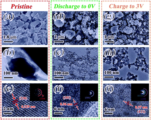 | ||
| Fig. 6 Ex situ SEM, TEM, HRTEM and corresponding SAED patterns (insets) of InSb in different states. (a–c) Pristine state; (d–f) discharge to 0 V; (g–i) charge to 3 V. | ||
4. Conclusion
In this paper, we use commercially available InSb alloy powder to carry out the research. The InSb can effectively reduce defects caused by pure In and Sb metals. In terms of long-term cycling properties, InSb delivers a specific charge capacity of 535.5 mA h g−1 at 400 mA g−1 after 80 cycles, corresponding to 78.6% capacity retention. Furthermore, in situ XRD, ex situ XPS, and ex situ TEM/HRTEM are applied to systematically explore the reaction mechanism of InSb. The results suggest that the InSb alloy anode exhibits extraordinary structural reversibility in the process of lithiation/delithiation. As a result, these merits make it an appealing anode host for the advancement of LIBs.Conflicts of interest
There are no conflicts to declare.Acknowledgements
This work is sponsored by NSAF (U1830106), the Laboratory of Precision Manufacturing Technology, the China Academy of Engineering Physics (ZD17006) and the K. C. Wong Magna Fund in Ningbo University.References
- M. Armand and J. M. Tarascon, Nature, 2008, 451, 652–657 CrossRef CAS PubMed.
- H. L. Tang, X. Qi, W. J. Han, L. Ren, Y. D. Liu, X. Y. Wang and J. X. Zhong, Appl. Surf. Sci., 2015, 355, 7–13 CrossRef CAS.
- L. Yan, H. Lan, H. X. Yu, S. S. Qian, X. Cheng, N. B. Long, R. F. Zhang, M. Shui and J. Shu, J. Mater. Chem. A, 2017, 5, 8972–8980 RSC.
- D. Wang, C. M. Zhang, Y. Y. Zhang, J. Wang and D. N. He, Ceram. Int., 2013, 39, 5145–5149 CrossRef CAS.
- R. T. Zheng, S. S. Qian, X. Cheng, H. X. Yu, N. Peng, T. T. Liu, J. D. Zhang, M. T. Xia, H. J. Zhu and J. Shu, Nano Energy, 2019, 58, 399–409 CrossRef CAS.
- P. Zhou, X. Wang, W. H. Guan, D. Zhang, L. B. Fang and Y. Z. Jiang, ACS Appl. Mater. Interfaces, 2017, 9, 6979–6987 CrossRef CAS PubMed.
- C. Wang, S. A. Wang, Y. B. He, L. K. Tang, C. P. Han, C. Yang, M. Wagemaker, B. H. Li, Q. H. Yang, J. K. Kim and F. Y. Kang, Chem. Mater., 2015, 27, 5647–5656 CrossRef CAS.
- M. Kitta, T. Akita, S. Tanaka and M. Kohyama, J. Power Sources, 2013, 237, 26–32 CrossRef CAS.
- G. E. Luo, J. R. He, X. J. Song, X. Y. Huang, X. Y. Yu, Y. P. Fang and D. Y. Chen, J. Alloys Compd., 2015, 621, 268–273 CrossRef CAS.
- H. X. Yu, H. Lan, L. Yan, S. H. Qian, X. Cheng, H. J. Zhu, N. B. Long, M. Shui and J. Shu, Nano Energy, 2017, 38, 109–117 CrossRef CAS.
- B. B. Wu, J. Lochala, T. Taverne and J. Xiao, Nano Energy, 2017, 40, 34–41 CrossRef CAS.
- R. Akolkar, J. Power Sources, 2013, 232, 23–28 CrossRef CAS.
- X. Cheng, H. J. Zhu, H. X. Yu, W. Q. Ye, R. T. Zheng, T. T. Liu, N. Peng, M. Shui and J. Shu, J. Mater. Chem. A, 2018, 6, 8620–8632 RSC.
- H. J. Zhu, X. Cheng, H. X. Yu, W. Q. Ye, N. Peng, R. T. Zheng, T. T. Liu, M. Shui and J. Shu, Nano Energy, 2018, 52, 192–202 CrossRef CAS.
- H. X. Wei, J. Yang, Y. F. Zhang, Y. Qian and H. B. Geng, J. Colloid Interface Sci., 2018, 524, 256–262 CrossRef CAS PubMed.
- W. Zhang, J. J. Yin, F. Q. Min, L. L. Jia, D. M. Zhang, Q. S. Zhang and J. Y. Xie, J. Mol. Struct., 2017, 1127, 777–783 CrossRef CAS.
- D. Zhang, B. Q. Wang, Y. Z. Jiang, P. Zhou, Z. H. Chen, B. Xu and M. Yan, J. Alloys Compd., 2015, 653, 604–610 CrossRef CAS.
- J. L. Gomez-Camer, C. Villevieille and P. Novak, J. Mater. Chem. A, 2013, 1, 13011–13016 RSC.
- G. Huang, F. F. Zhang, X. C. Du, Y. L. Qin, D. M. Yin and L. M. Wang, ACS Nano, 2015, 9, 1592–1599 CrossRef CAS PubMed.
- Y. C. Fang, Y. D. Huang, S. Zhang, W. Jia, X. C. Wang, Y. Guo, D. Z. Jia and L. S. Wang, Chem. Eng. J., 2017, 315, 583–590 CrossRef CAS.
- N. Nitta and G. Yushin, Part. Part. Syst. Charact., 2014, 31, 317–336 CrossRef CAS.
- C. M. Park, J. H. Kim, H. Kim and H. J. Sohn, Chem. Soc. Rev., 2010, 39, 3115–3141 RSC.
- Y. Z. Jiang, Y. Li, P. Zhou, Z. Y. Lan, Y. H. Lu, C. Wu and M. Yan, Adv. Mater., 2017, 29, 1606499 CrossRef PubMed.
- I. Rom, M. Wachtler, I. Papst, M. Schmied, J. O. Besenhard, F. Hofer and M. Winter, Solid State Ionics, 2001, 143, 329–336 CrossRef CAS.
- C. S. Johnson, J. T. Vaughey, M. M. Thackeray, T. Sarakonsri, S. A. Hackney, L. Fransson, K. Edström and J. O. Thomas, Electrochem. Commun., 2000, 2, 595–600 CrossRef CAS.
- L. M. L. Fransson, J. T. Vaughey, R. Benedek, K. Edström, J. O. Thomas and M. M. Thackeray, Electrochem. Commun., 2001, 3, 317–323 CrossRef CAS.
- M. Wachtler, M. Winter and J. O. Besenhard, J. Power Sources, 2002, 105, 151–160 CrossRef CAS.
- J. T. Vaugheya, L. Franssonb, H. A. Swingera, K. Edströmb and M. M. Thackeray, J. Power Sources, 2003, 119–121, 64–68 CrossRef.
- W. J. Zhang, J. Power Sources, 2011, 196, 877–885 CrossRef CAS.
- J. O. Besenhard, J. Yang and M. Winter, J. Power Sources, 1997, 68, 87–90 CrossRef CAS.
- H. Li, Z. X. Wang, L. Q. Chen and X. J. Huang, Adv. Mater., 2009, 21, 4593–4607 CrossRef CAS.
- S. O. Kim and A. Manthiram, ACS Appl. Mater. Interfaces, 2015, 7, 14801–14807 CrossRef CAS PubMed.
- I. T. Kim, Sci. Adv. Mater., 2016, 8, 80–83 CrossRef CAS.
- C. M. Park, S. Yoon, S. I. Lee, J. H. Kim, J. H. Jung and H. J. Sohn, J. Electrochem. Soc., 2007, 154, A917–A920 CrossRef CAS.
- Y. Wang and J. Y. Lee, Angew. Chem., Int. Ed., 2006, 45, 7039–7042 CrossRef CAS PubMed.
- K. H. Nam and C. M. Park, J. Mater. Chem. A, 2016, 4, 8562–8565 RSC.
- Y. B. Zhao and A. Manthiram, Chem. Mater., 2015, 27, 3096–3101 CrossRef CAS.
- Q. C. Pan, Y. N. Wu, F. H. Zheng, X. Ou, C. H. Yang, X. H. Xiong and M. L. Liu, Chem. Eng. J., 2018, 348, 653–660 CrossRef CAS.
- E. Allcorn and A. Manthiram, ACS Appl. Mater. Interfaces, 2014, 6, 10886–10891 CrossRef CAS PubMed.
- H. S. Hou, X. Y. Cao, Y. C. Yang, L. B. Fang, C. C. Pan, X. M. Yang, W. X. Song and X. B. Ji, Chem. Commun., 2014, 50, 8201–8203 RSC.
- T. Yang, H. Wang, J. T. Xu, L. Wang, W. C. Song, Y. H. Mao and J. M. Ma, RSC Adv., 2016, 6, 78959–78962 RSC.
- K. Wang, P. Qin, Z. H. Ge and J. Feng, Mater. Lett., 2017, 209, 373–375 CrossRef CAS.
- H. Wang, H. X. Yang and L. Lu, RSC Adv., 2014, 4, 17483–17489 RSC.
- O. Crosnier, T. Brousse, X. Devaux, P. Fragnaud and D. M. Schleich, J. Power Sources, 2001, 94, 169–174 CrossRef CAS.
- C. H. Kuo, J. M. Wu and S. J. Lin, Nanoscale Res. Lett., 2013, 8, 1–8 CrossRef PubMed.
- K. E. Hnida, S. Bäßler, J. Mech, K. Szacilowski, R. P. Socha, M. Gajewska, K. Nielsch, M. Przybylski and G. D. Sulka, J. Mater. Chem. C, 2016, 4, 1345–1350 RSC.
- J. Yang, Y. Takeda, N. Imanishi, T. Ichikawa and O. Yamamoto, Solid State Ionics, 2000, 135, 175–180 CrossRef CAS.
- I. Rom, M. Wachtler, I. Papst, M. Schmied, J. O. Besenhard, F. Hofer and M. Winter, Solid State Ionics, 2001, 143, 329–336 CrossRef CAS.
- F. H. Zheng, W. T. Zhong, Q. Deng, Q. C. Pan, X. Ou, Y. Z. Liu, X. H. Xiong, C. H. Yang, Y. Chen and M. L. Lite, Chem. Eng. J., 2019, 357, 226–236 CrossRef CAS.
- L. Yan, J. Shu, C. X. Li, X. Cheng, H. J. Zhu, H. X. Yu, C. F. Zhang, Y. Zheng, Y. Xie and Z. P. Guo, Energy Storage Materials, 2019, 16, 535–544 CrossRef.
Footnotes |
| † Electronic supplementary information (ESI) available. See DOI: 10.1039/c9se00429g |
| ‡ These authors contributed equally to this work. |
| This journal is © The Royal Society of Chemistry 2019 |

