
First-principles investigation of the Schottky contact for the two-dimensional MoS2 and graphene heterostructure
Biao Liu,
Li-Juan Wu,
Yu-Qing Zhao,
Ling-Zhi Wang and
Meng-Qiu Cai*
School of Physics and Electronics Science, Hunan University, Changsha, Hunan 410082, People’s Republic of China. E-mail: mqcai@hnu.edu.cn; Tel: +86 731 88821177
First published on 15th June 2016
Abstract
The electronic properties of an MoS2 and graphene heterostructure are investigated by density functional calculations. Our results show that both the intrinsic properties of MoS2 and graphene at the equilibrium interfacial distance are preserved in the weak van der Waals contact. Furthermore, Schottky doping for the MoS2 and graphene contact can be tuned by the interfacial distance. Our calculations show that the Schottky doping can be transformed from an n-type Schottky contact to a p-type Schottky contact when the interfacial distance decreased. We find that interfacial charge transfer and the Fermi level shift determines the Schottky barrier transition from an n-type Schottky contact to a p-type Schottky contact. Our studies may prove to be instrumental in the future design and fabrication of van der Waals based field effect transistors.
1 Introduction
Two-dimensional (2D) materials have received considerable attention owing to their extraordinary electronic, optical, mechanical, chemical, and thermal properties, which make these materials promising for next-generation optoelectronic and nanoelectronic devices.1–7 The very first material that boosted research in the area 2D materials was graphene.8 Graphene, a 2D sp2-hybridized carbon monolayer, is known to have many remarkable properties, such as a high carrier mobility.9,10 However, the gapless nature of monolayer graphene has restrained its wide application in electronic devices. Later, a whole new class of 2D materials has been studied, namely the transition metal dichalcogenides (TMDs).11 MoS2 is one of the most studied TMDs. Bulk MoS2 has a layered structure with a weak van der Waals (vdW) attraction between the layers. Unlike gapless graphene, monolayer MoS2 is a direct band-gap semiconductor with a band gap of ∼1.8 eV, whereas bulk MoS2 is an indirect band-gap semiconductor with a band gap of ∼1.3 eV.12,13 Furthermore, single-layer MoS2 owns a high on/off current ratio of about 108 and a high room-temperature carrier mobility of around 400 cm2 V−1 s−1, which enables applications in field-effect transistors (FETs), photodetectors, and electroluminescent devices.11,14,15Many researchers are studying the application of ultrathin MoS2 FETs. The application of ultrathin MoS2 FETs is mainly limited by the large contact resistance at MoS2/metal interfaces.16–19 Our previous study showed that the height of the Schottky barrier for the Pd–MoS2 contact can be tuned by different strains.16 Recent efforts have focused on taking advantage of the individual properties of different 2D materials by fabricating heterostructures, which are vertical stacks of 2D layers of dissimilar materials held together by vdW forces.20,21 These vdW heterostructures, such as graphene/MoS2 (G/MoS2),21–24 graphene/hexagonal boron nitride (G/h-BN),25–27 graphene/silicene (G/Si)28,29 and graphene/phosphorene (G/P), have been widely studied experimentally and theoretically, and can preserve the intrinsic electronic properties of the dissimilar 2D materials and create particularly advantageous electronic properties.20,30 Some research has shown that a nanodevice based on the MoS2–graphene vdW heterostructure has a light weight, a low power consumption and flexibility.31–33 The growth of MoS2 on graphene will increase the electron transfer rate and improve the electrochemical performance.34 The charge transfer, the Schottky barrier, and the work function can be controlled by an external electric field.35 In fact, the interfacial distance of a two-dimensional vdW heterostructure has an important impact on its electronic properties. For example, the electronic properties of the graphene/phosphorene interface can change from an n-type Schottky contact to a p-type Schottky contact.36 Therefore, we can investigate the effect on the electronic properties of the MoS2–graphene vdW heterostructure by varying the interfacial distance.
In the present work, we study the electronic properties of a MoS2 and graphene heterostructure by first-principles calculations. The intrinsic properties of the MoS2 and graphene layers are preserved in the weak vdW heterostructure at the equilibrium interfacial distance. Changing the interfacial distance can achieve the transition from an n-type Schottky contact to a p-type Schottky contact in the MoS2–graphene heterostructure. This shows that the interfacial charge transfer and the Fermi level shift determine the Schottky barrier transition. Our studies may prove to be instrumental in the future design and fabrication of vdW based field effect transistors.
2 Computational method and model
This article uses density-functional theory (DFT) with the projected augmented wave (PAW) method, as implemented within the Vienna Ab-Initio Simulation Package (VASP).37–40 The generalized gradient approximation (GGA) by the Perdew–Burke–Ernzerhof (PBE) functional is utilized as the exchange–correlation functional, which can reasonably predict the bandgap of MoS2.41 The vdW correction proposed by Grimme is included in our calculations due to its good description of long-range vdW interactions.42 The heterojunction calculations are performed by using the 5 × 5 × 1 Monkhorst–Pack K-point mesh and using an energy cutoff of 550 eV for the plane-wave expansion. All atoms are allowed to be fully relaxed until the atomic Hellmann–Feynman forces are smaller than 0.01 eV Å−1 and the convergence criterion of energy in the self-consistency process is set to 10−4 eV.The calculated lattice parameters of the pristine monolayer MoS2 and graphene are 3.16 Å and 2.46 Å, respectively. We choose MoS2 as a substrate to match with graphene. The unit cell of our system is composed of 5 × 5 unit cells of graphene and 4 × 4 unit cells of MoS2 along the X and Y directions, which can nicely match, as shown in Fig. 1. The lattice mismatch is ∼2.7% for the composed configuration. A vacuum space of 15 Å in the Z direction is used to avoid the interactions between neighboring slabs. The equilibrium geometry configuration of the system is depicted in Fig. 1a and b. The MoS2 layer combines with the graphene layer by vdW interactions and the interaction between the interlayers is weak in the heterostructure. To obtain the equilibrium configuration, we firstly fully relax the heterostructure along the X and Y directions. After finding the lowest energy configuration, we move the MoS2 layer with respect to the graphene layer by finite amounts δX, in order to make sure this is really the minimum energy configuration, as shown in Fig. 2. Because the configuration is symmetrical in the X and Y directions, we only show the data along the X direction. The results show that the fully relaxed configuration is the minimum energy configuration. After being fully relaxed along the X and Y directions of the MoS2–graphene configuration, we choose different interlayer distance d to re-optimize the configuration until we find a stable interlayer distance. The schematic of d is shown in Fig. 1b.
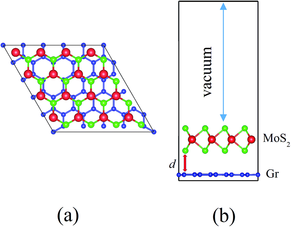 | ||
| Fig. 1 (a) Top view of the MoS2–graphene heterostructure. The C, S, and Mo atoms are shown as blue, green and red balls, respectively. (b) Side view of MoS2–graphene contact heterostructure. The interlayer distance d is shown. The vacuum is marked by the double arrow. | ||
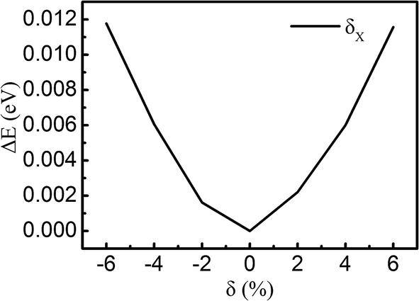 | ||
| Fig. 2 Evolution of the total energy as a function of displacement δX of the MoS2 layer relative to graphene, taking the origin at the lowest energy configuration. | ||
3 Results and discussion
The electronic properties of monolayer MoS2 and pristine graphene were checked first and the energy band structures are plotted in Fig. 3a and b. It shows that the monolayer MoS2 is a direct bandgap semiconductor at the K point with a band gap of 1.67 eV via the PBE functional, and that graphene has no distinguishable bandgap and retains its metallic character, which agrees well with previous theoretical studies.9,10 We also used the hybrid Heyd–Scuseria–Ernzerhof (HSE) functional to calculate the bandgap of monolayer MoS2 and the bandgap was 2.32 eV, which obviously exceeds the experimental value of 1.8 eV. After fully relaxing the MoS2–graphene heterostructure by the PBE functional and vdW correction, we find that the equilibrium interfacial distance value is 3.37 Å, which is also in accordance with previous theoretical studies.17 According to the long interfacial distance value, we infer that the interfacial interaction will be very weak.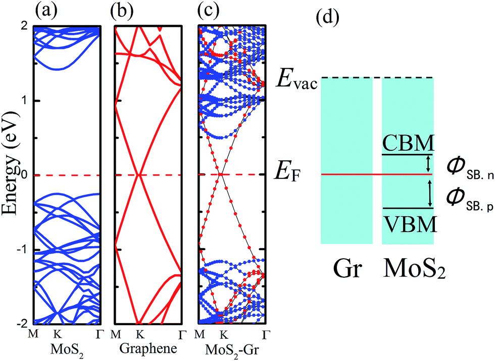 | ||
| Fig. 3 Electronic band structures of (a) MoS2 monolayer, (b) graphene and (c) MoS2–graphene heterostructure. The Fermi level is set to zero and marked by red dotted lines. (d) A schematic of the MoS2–graphene interface Schottky contact. The n-type or p-type SBH are indicated between the conduction band minimum or the valence band maximum of the MoS2 layer and the Fermi level. | ||
To quantitatively characterize the mechanical properties of the interface, the binding energy (Eb) per carbon atom between the MoS2 monolayer and the graphene sheet is calculated as Eb = [EMoS2/Gr − (EMoS2 + EGr)]/Nc, where EMoS2/Gr is the total energy of the MoS2 monolayer and graphene sheet heterostructure, EMoS2 is the total energy of the isolated MoS2 monolayer, EGr is the total energy of the isolated graphene layer and Nc = 50 is the number of carbon atoms in the unit cell. At the optimum spacing, the calculated binding energy per C atom is −28.2 meV, which agrees well with a previous theoretical study.21 According to the negligible binding energy, the graphene is found to interact very weakly with the MoS2 monolayer. The results suggest that the graphene is bound to MoS2 via vdW interactions.
The calculated electronic band structures of the MoS2–graphene heterostructures at the equilibrium interfacial distance are displayed in Fig. 3c. Blue and red denote the contributions from the MoS2 monolayer and graphene sheet, respectively. Compared with the energy band structures of the monolayer MoS2 and pristine graphene shown in Fig. 3a and b, respectively, the electronic structure of the MoS2–graphene heterostructure seems to be a simple sum of each constituent. The integral shape of the band structures of the MoS2–graphene heterostructure is basically in accordance with the sum of those of the monolayer MoS2 and pristine graphene. In addition, it demonstrates that a vacuum space of 15 Å in the Z direction is enough to avoid the interactions between neighboring slabs. The band contributed by MoS2 illustrates that the MoS2 layer maintains the direct bandgap at the K point with a bandgap of 1.66 eV, and the band contributed by graphene illustrates that the graphene layer maintains its metallic character. Therefore, the dominant sorts of binding forces at the MoS2–graphene interface are vdW interactions. The MoS2–graphene heterostructure will preserve the intrinsic excellent electronic properties of the dissimilar 2D materials.
The MoS2–graphene configuration is a representative metal–semiconductor (MS) heterojunction. The electrical current flowing across the interface between metal and semiconductor is usually non-linear against the applied bias voltage. For n-type semiconductors, electrons near its conduction band minimum (CBM) are primarily responsible for electrical conduction, and for p-type semiconductors, holes near the valence band maximum (VBM) carry the most of the current. At the MS interface, the electrons of the lowest-lying states (located at the CBM) for the n-type semiconductor can spontaneously flow to the metal. When electronic transport occurs across the MS interface, the states will be offset, known as the n-type Schottky barrier height (SBH) which is shown in Fig. 3d. The barrier can lead to rectifying behavior between the metal and n-type semiconductor. The flow of electrons from the semiconductor to the metal is easier than conduction in the opposite direction. If the p-type semiconductor is in contact with the metal, the energy difference between the Fermi level and the VBM is the p-type SBH, also shown in Fig. 3d. The p-type SBH controls the transport of holes across this MS interface. Because the current flow across the MS interface depends on the magnitude of the SBH, the SBH is clearly the most important property of a MS interface. Therefore, it is necessary to study the SBH of the MoS2–graphene interface. After analysis of the band structure of the MoS2–graphene heterojunction, shown in Fig. 3c, we find that the n-type SBH is 0.49 eV.
We apply a dissimilar interfacial distance to the MoS2–graphene configuration in order to explore the interface electronic properties. Note that it is challenging to tune the interlayer distance in the experiments, but we only demonstrate the effect of interlayer distance on the electronic structure and provide useful insight into the electronic engineering of this nanocomposite material. The band structures are shown in Fig. 4 under different interfacial distances. As the interfacial distance is changed greatly from 4.0 Å to 2.8 Å, the shape of the band changes slightly, however, the Fermi level descends relatively gradually. The magnitude of the energy level of MoS2’s CBM exceeds that of the VBM gradually. This result shows that the Schottky doping of graphene is transformed from an n-type Schottky contact to a p-type Schottky contact when the interfacial distance is decreased.
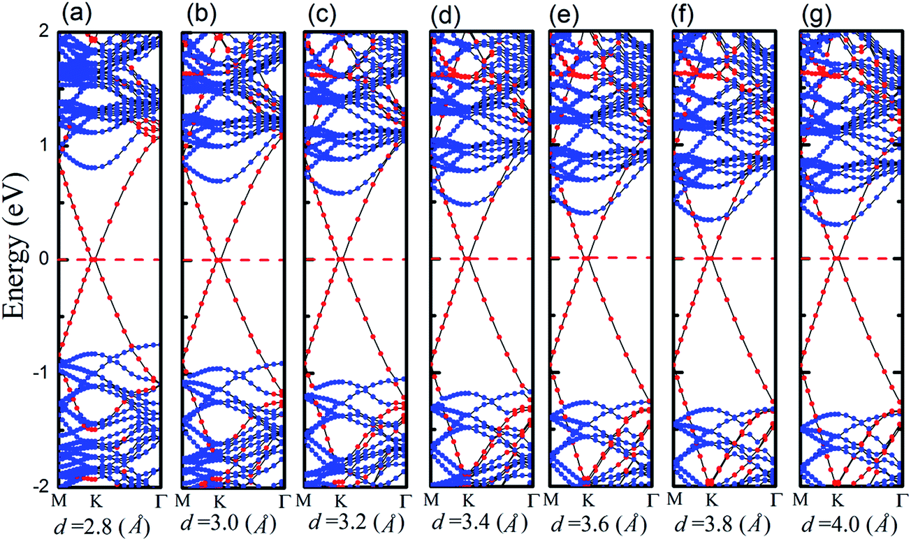 | ||
| Fig. 4 Band structures of the MoS2–graphene heterostructure under different interface distance. Blue and red denote the contributions from MoS2 monolayers and graphene, respectively. (a)–(g) represent the interface distances of 2.8 Å, 3.0 Å, 3.2 Å, 3.4 Å, 3.6 Å, 3.8 Å, and 4.0 Å, respectively. The Fermi level is set to zero and marked by red dotted lines. | ||
To quantitatively characterize SBH and Schottky doping for the MoS2–graphene contact, the evolution of the CBM, VBM and bandgap of MoS2 as a function of the interfacial distance is shown in Fig. 5. With the decrease in interfacial distance from 4.0 Å to 2.8 Å, the magnitudes of the VBM gradually decrease and the magnitudes of the CBM gradually increase. As a result, the lines of the CBM and VBM intersect between interfacial distances of 3 Å and 2.8 Å, where the Schottky barrier is transformed from an n-type Schottky contact to a p-type Schottky contact. After fitting the data in Fig. 5, the transition of the Schottky barrier is located at the interfacial distance of 2.85 Å. The n-type SBH is 0.298 eV, 0.339 eV, 0.397 eV, 0.477 eV, 0.578 eV and 0.695 eV under the interfacial distance of 4 Å, 3.8 Å, 3.6 Å, 3.4 Å, 3.2 Å and 3 Å, respectively, and the p-type SBH is 0.748 eV under the interfacial distance of 2.8 Å. Therefore, the interfacial distance can not only tune the SBH, but also achieve the Schottky barrier transition from an n-type Schottky contact to a p-type Schottky contact.
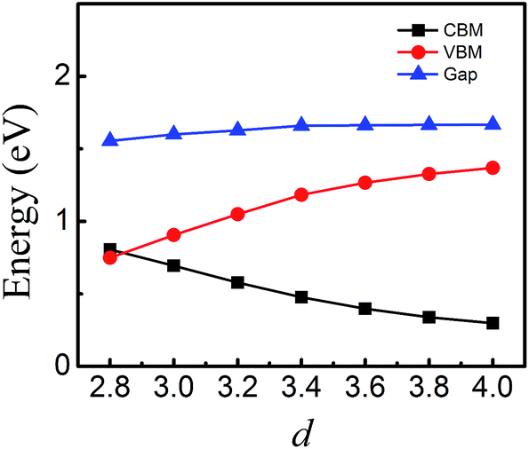 | ||
| Fig. 5 CBM, VBM and band gap of MoS2 monolayer in the MoS2–graphene heterostructure as a function of interfacial distance. | ||
As the graphene electrode comes into contact with the MoS2 monolayer, the heterostructure becomes a unified electronic system. Even without any charge transfer between the MoS2 and graphene systems, there will be a small band bending. The band bending can be defined as ΔW = W − WMoS2, where W is the work function of the composed system and WMoS2 is the work function of the pristine monolayer MoS2. The calculated work functions of the composed system are 5.03 eV and 4.74 eV under interfacial distances of 2.8 Å and 3.8 Å, respectively. The work function of the pristine monolayer MoS2 is 4.92 eV. The band bending is 0.11 eV for the interfacial distance of 2.8 Å and −0.18 eV for the interfacial distance of 3.8 Å. As ΔW > 0, electrons will be transferred from the non-contacted MoS2 region to the MoS2 and graphene one, making the channel p-type. As ΔW < 0, the results are opposite, which predict an n-type contact.
As the interfacial distance decreases from 4 Å to 2.8 Å, the effects of chemical interactions and charge transfer between MoS2 and graphene are enhanced, which may result in the Schottky barrier conversion. Because of the interfacial interaction between the MoS2 and graphene layers, a pronounced shift of the graphene Fermi level relative to MoS2 exists, which was observed in a previous study.16 The Fermi level shift can be induced by charge transfer at the interface. To illustrate the detailed nature of the charge transfer and the Fermi level shift at the MoS2–graphene interface, we plot the plane-averaged charge density difference Δρ(z) along the perpendicular direction to the interface, which can provide a quantitative picture of the charge redistribution at the interface. The plane-averaged charge density difference can be written as Δρ(z) = ρMoS2/graphene − ρgraphene − ρMoS2. Here, ρMoS2/graphene is the plane-averaged density of the combined MoS2–graphene system, and ρMoS2 and ρgraphene are the plane-averaged densities of the isolated MoS2 and graphene layers, respectively, which are calculated by freezing the atomic positions of the respective components in the combined system. As shown in Fig. 6a and b, Δρ(z) has been plotted under interfacial distances of 2.8 Å and 3.8 Å, respectively. The red color filled areas represent a charge accumulation region and the blue regions represent charge depletion. The plane-averaged charge density difference at 2.8 Å is much more pronounced, with the charge density difference more than 10 times larger than at 3.8 Å, resulting in much greater electron transfer from graphene to the MoS2 layer. Compared to the case with the interface distance at 2.8 Å, the interface net charge accumulation is translated from the MoS2 layers to graphene layers in the MoS2–graphene heterostructures with the interface distance at 3.8 Å. As a result, a shift in the Fermi level occurs. The Fermi level shift can achieve the transition of the Schottky barrier from an n-type Schottky contact to a p-type Schottky contact in MoS2–graphene heterostructures under different interface distances. Besides, the work function is changed in the MoS2–graphene heterostructures upon changing the interface distance from 2.8 Å to 3.8 Å. The work function is defined as the energy difference between the vacuum potential and the Fermi level. The calculated work functions at 2.8 Å and 3.8 Å are 4.97 eV and 4.59 eV, respectively. The results reveal that the Fermi level shifts upward to the CBM of the MoS2 layer moving from an interface distance of 2.8 Å to 3.8 Å in the MoS2–graphene heterostructures. Therefore, the interfacial charge transfer and the Fermi level shift are the reasons for the transition of the Schottky barrier from an n-type Schottky contact to a p-type Schottky contact in MoS2–graphene heterostructures under different interface distances from 4.0 Å to 2.8 Å.
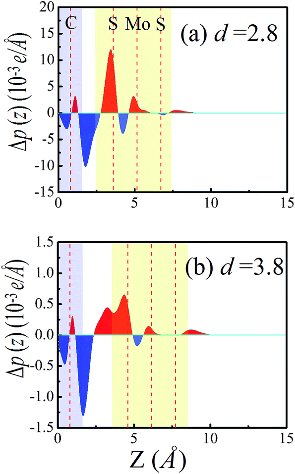 | ||
| Fig. 6 Plots of the plane-averaged electron density difference along the direction perpendicular to the interface of the MoS2–graphene heterostructure under different interface distances of 2.8 Å (a) and 3.8 Å (b), respectively. The red and blue colors indicate electron accumulation and depletion, respectively. | ||
4 Conclusions
In summary, with first-principles calculations, we have systematically and comprehensively investigated the electronic properties of a MoS2–graphene vdW heterostructure while varying the interfacial distance. We found that MoS2 interacts weakly with graphene via weak vdW interactions to preserve its intrinsic electronic properties at the equilibrium interfacial distance. Furthermore, the interfacial distance has a great influence on the Schottky barrier doping. Tuning the interfacial distance between the MoS2 and graphene can achieve the Schottky barrier transition from an n-type Schottky contact to a p-type Schottky contact. We found that the interfacial charge transfer and the Fermi level shift determine the Schottky barrier transition in the MoS2–graphene heterostructure. Our studies may prove to be instrumental in the future design and fabrication of vdW based field effect transistors.Acknowledgements
The authors express their thanks to the Changsha Supercomputer Center for computation. This work has been supported by the National Natural Science Foundation of China through Grant No. 51172067, the Hunan Provincial Natural Science Fund for Distinguished Young Scholars through Grant No. 13JJ1013, the Specialized Research Fund for the Doctoral Program of Higher Education through Grant No. 20130161110036, and the New Century Excellent Talents in University through Grant NCET-12-0171. D.References
- D. Xiao, G. B. Liu, W. X. Feng, X. D. Xu and W. Yao, Phys. Rev. Lett., 2012, 108, 196802 CrossRef PubMed.
- Z. Y. Zhu, Y. C. Cheng and U. Schwingenschlogl, Phys. Rev. B: Condens. Matter Mater. Phys., 2011, 84, 153402 CrossRef.
- Q. H. Wang, K. Kalantar-Zadeh, A. Kis, J. N. Coleman and M. S. Strano, Nat. Nanotechnol., 2012, 7, 699–712 CrossRef CAS PubMed.
- J. N. Coleman, M. Lotya, A. O’Neill, S. D. Bergin, P. J. King, U. Khan, K. Young, A. Gaucher, S. De, R. J. Smith, I. V. Shvets, S. K. Arora, G. Stanton, H. Y. Kim, K. Lee, G. T. Kim, G. S. Duesberg, T. Hallam, J. J. Boland, J. J. Wang, J. F. Donegan, J. C. Grunlan, G. Moriarty, A. Shmeliov, R. J. Nicholls, J. M. Perkins, E. M. Grieveson, K. Theuwissen, D. W. McComb, P. D. Nellist and V. Nicolosi, Science, 2011, 331, 568–571 CrossRef CAS PubMed.
- H. Shu, P. Luo, P. Liang, D. Cao and X. Chen, ACS Appl. Mater. Interfaces, 2015, 7, 7534–7541 Search PubMed.
- D. Cao, T. Shen, P. Liang, X. Chen and H. Shu, J. Phys. Chem. C, 2015, 119, 4294–4301 CrossRef CAS.
- H. Shu, F. Li, C. Hu, P. Liang, D. Cao and X. Chen, Nanoscale, 2016, 8, 2918–2926 RSC.
- K. S. Novoselov, A. K. Geim, S. V. Morozov, D. Jiang, M. I. Katsnelson, I. V. Grigorieva, S. V. Dubonos and A. A. Firsov, Nature, 2005, 438, 197–200 CrossRef CAS PubMed.
- A. H. Castro Neto, F. Guinea, N. M. R. Peres, K. S. Novoselov and A. K. Geim, Rev. Mod. Phys., 2009, 81, 109–162 CrossRef CAS.
- A. C. Ferrari, J. C. Meyer, V. Scardaci, C. Casiraghi, M. Lazzeri, F. Mauri, S. Piscanec, D. Jiang, K. S. Novoselov, S. Roth and A. K. Geim, Phys. Rev. Lett., 2006, 97, 187401 CrossRef CAS PubMed.
- B. Radisavljevic, A. Radenovic, J. Brivio, V. Giacometti and A. Kis, Nat. Nanotechnol., 2011, 6, 147–150 CrossRef CAS PubMed.
- K. F. Mak, C. Lee, J. Hone, J. Shan and T. F. Heinz, Phys. Rev. Lett., 2010, 105, 136805 CrossRef PubMed.
- T. Eknapakul, P. D. C. King, M. Asakawa, P. Buaphet, R. H. He, S. K. Mo, H. Takagi, K. M. Shen, F. Baumberger, T. Sasagawa, S. Jungthawan and W. Meevasana, Nano Lett., 2014, 14, 1312–1316 CrossRef CAS PubMed.
- Y. Yoon, K. Ganapathi and S. Salahuddin, Nano Lett., 2011, 11, 3768–3773 CrossRef CAS PubMed.
- D. Jena and A. Konar, Phys. Rev. Lett., 2007, 98, 136805 CrossRef PubMed.
- B. Liu, L. J. Wu, Y. Q. Zhao, L. Z. Wang and M. Q. Cai, Phys. Chem. Chem. Phys., 2015, 17, 27088–27093 RSC.
- J. H. Kang, W. Liu, D. Sarkar, D. Jena and K. Banerjee, Phys. Rev. X, 2014, 4, 031005 Search PubMed.
- L. P. Feng, J. Su, D. P. Li and Z. T. Liu, Phys. Chem. Chem. Phys., 2015, 17, 6700–6704 RSC.
- B. Liu, L. J. Wu, Y. Q. Zhao, L. Z. Wang and M. Q. Cai, Eur. Phys. J. B, 2016, 89, 80 CrossRef.
- J. E. Padilha, A. Fazzio and A. J. R. da Silva, Phys. Rev. Lett., 2015, 114, 066803 CrossRef CAS PubMed.
- Y. D. Ma, Y. Dai, M. Guo, C. W. Niu and B. B. Huang, Nanoscale, 2011, 3, 3883–3887 RSC.
- X. D. Li, S. Yu, S. Q. Wu, Y. H. Wen, S. Zhou and Z. Z. Zhu, J. Phys. Chem. C, 2013, 117, 15347–15353 CrossRef CAS.
- L. Britnell, R. M. Ribeiro, A. Eckmann, R. Jalil, B. D. Belle, A. Mishchenko, Y. J. Kim, R. V. Gorbachev, T. Georgiou, S. V. Morozov, A. N. Grigorenko, A. K. Geim, C. Casiraghi, A. H. Castro Neto and K. S. Novoselov, Science, 2013, 340, 1311–1314 CrossRef CAS PubMed.
- H. Tian, Z. Tan, C. Wu, X. M. Wang, M. A. Mohammad, D. Xie, Y. Yang, J. Wang, L. J. Li, J. Xu and T. L. Ren, Sci. Rep., 2014, 4, 5951 CrossRef CAS PubMed.
- C. R. Dean, A. F. Young, I. Meric, C. Lee, L. Wang, S. Sorgenfrei, K. Watanabe, T. Taniguchi, P. Kim, K. L. Shepard and J. Hone, Nat. Nanotechnol., 2010, 5, 722–726 CrossRef CAS PubMed.
- X. Lin, Y. Xu, A. A. Hakro, T. Hasan, R. Hao, B. L. Zhang and H. S. Chen, J. Mater. Chem. C, 2013, 1, 1618–1627 RSC.
- J. M. Xue, J. Sanchez-Yamagishi, D. Bulmash, P. Jacquod, A. Deshpande, K. Watanabe, T. Taniguchi, P. Jarillo-Herrero and B. J. Leroy, Nat. Mater., 2011, 10, 282–285 CrossRef CAS PubMed.
- M. Neek-Amal, A. Sadeghi, G. R. Berdiyorov and F. M. Peeters, Appl. Phys. Lett., 2013, 103, 261904 CrossRef.
- Y. Cai, C. P. Chuu, C. M. Wei and M. Y. Chou, Phys. Rev. B: Condens. Matter Mater. Phys., 2013, 88, 245408 CrossRef.
- W. Hu, T. Wang and J. L. Yang, J. Mater. Chem. C, 2015, 3, 4756–4761 RSC.
- S. Bertolazzi, D. Krasnozhon and A. Kis, ACS Nano, 2013, 7, 3246–3252 CrossRef CAS PubMed.
- L. L. Yu, Y. H. Lee, X. Ling, E. J. G. Santos, Y. C. Shin, Y. X. Lin, M. Dubey, E. Kaxiras, J. Kong, H. Wang and T. Palacios, Nano Lett., 2014, 14, 3055–3063 CrossRef CAS PubMed.
- K. Roy, M. Padmanabhan, S. Goswami, T. P. Sai, G. Ramalingam, S. Raghavan and A. Ghosh, Nat. Nanotechnol., 2013, 8, 826–830 CrossRef CAS PubMed.
- K. Chang and W. X. Chen, Chem. Commun., 2011, 47, 4252–4254 RSC.
- X. G. Liu and Z. Y. Li, J. Phys. Chem. Lett., 2015, 6, 3269–3275 CrossRef CAS.
- C. J. Jin, F. A. Rasmussen and K. S. Thygesen, J. Phys. Chem. C, 2015, 119, 19928–19933 CrossRef CAS.
- G. Kresse and J. Furthmuller, Phys. Rev. B: Condens. Matter Mater. Phys., 1996, 54, 11169–11186 CrossRef CAS.
- P. E. Blochl, Phys. Rev. B: Condens. Matter Mater. Phys., 1994, 50, 17953–17979 CrossRef.
- M.-Q. Cai, Y.-J. Zhang, Z. Yin and M.-S. Zhang, Phys. Rev. B: Condens. Matter Mater. Phys., 2005, 72, 075406 CrossRef.
- Y.-Q. Zhao, L.-J. Wu, B. Liu, L.-Z. Wang, P.-B. He and M.-Q. Cai, J. Power Sources, 2016, 313, 96–103 CrossRef CAS.
- L. Y. Gan, Q. Y. Zhang, Y. C. Cheng and U. Schwingenschlogl, Phys. Rev. B: Condens. Matter Mater. Phys., 2013, 88, 235310 CrossRef.
- S. Grimme, J. Comput. Chem., 2006, 27, 1787–1799 CrossRef CAS PubMed.
| This journal is © The Royal Society of Chemistry 2016 |