DOI:
10.1039/C6RA02390H
(Paper)
RSC Adv., 2016,
6, 24675-24682
Tailoring the electrical and photo-electrical properties of a WS2 field effect transistor by selective n-type chemical doping†
Received
26th January 2016
, Accepted 25th February 2016
First published on 26th February 2016
Abstract
Here, we demonstrate a doping technique which remarkably improves the electrical and photoelectric characteristics of a WS2 field effect transistor (FET) by chemical doping. The shift of the threshold voltage towards a negative gate voltage and the red shift of the E12g and A1g peaks in the Raman spectra confirm the n-type doping effect in WS2 FETs. WS2 films show an unprecedented high mobility of 255 cm2 V−1 s−1 at room temperature. The on/off ratio of the output current is ∼108 at room temperature. The mobility of a multilayer ML-WS2 FET was found to be 425 cm2 V−1 s−1 at 5 K. Semiconductor-to-metal transitions were also observed at Vbg > 30 V. A decrease in contact and sheet resistance was observed after potassium iodide (KI) doping. The photocurrent in WS2 FETs was also enhanced after n-type doping. Chemical doping exhibited a very stable, effective, and easy-to-apply method to enhance the performance of a WS2 FET.
1. Introduction
Due to unique physical and electrical properties,1,2 considerable interest has developed for two-dimensional (2D) atomic layered materials.3,4 Graphene, an exemplary 2D carbon system with fascinating properties, which makes it a promising material in a variety of future nanoelectronics applications such as field effect transistors (FETs),5 ultracapacitors, solar cells and especially as gas and chemical sensors.6 Regardless of all its advantages in nanoelectronics device applications, graphene cannot be used as an active channel material in FETs due to the absence of a bandgap.7 Considerable research efforts have been conducted to attain a significant bandgap in graphene like patterning into nanoribbons,7 chemical functionalization,8 and dual-gated bilayer graphene.9 But it always shows bandgap versus significant mobility degradation with low on/off switching ratio for FETs.10 Recently, the absence of a bandgap in graphene has encouraged researchers to search for other 2D layered materials.
2D tungsten disulphide (WS2) is a tremendous material provoking as strong competitors for next-generation nanoelectronics and optoelectronics devices. WS2 is of atomic-layer-thick that does have a bandgap.11 It has specific interest due to transition of indirect-to-direct bandgap nature by changing number of layers and observation of photoluminescence (PL) in the visible range at room temperature.12,13 Bulk WS2 is an n-type semiconductor with an indirect-bandgap (1.4 eV), but turn into a direct-bandgap (2.1 eV) material when cleaved as monolayer.14 WS2 is 2D layered semiconductor material; it has been widely studied due to its attractive electrical and optical properties in a variety of applications.15 Especially in the field of low power FET,16 photodectors,17 gas and chemical sensors,18 memory and electroluminescent devices, and integrated circuits.11,19
Like other low-dimensional semiconductors transport properties of WS2 are strongly degraded by the extrinsic/environmental effects, which limit their intrinsic properties and overall permanence.20,21 It has been already exposed that the electrical and photoelectrical characteristics of a mechanically exfoliated WS2 layer could be affected by the adsorbents in ambient air.22 The improvement in sample quality is essential for the upcoming development of WS2 device technology.11 Recently, different strategies were used to improve the device performance by limiting the Schottky barrier height (SBH) by using different contact electrode,23,24 and with different substrate to enhance charge carrier mobility.25 Different doping techniques are used to control the carrier concentrations in 2D semiconductor materials.26 The controlled doping of WS2 layers is important for controlling the carrier concentrations, which has fundamental significance for FET devices. Such efforts are extremely crucial for WS2-based FETs and related electronic device design, to curtailed environment effect in order to improve the device performance. Chemical doping is the most effective and easy method for tuning the electrical and photoelectrical properties of semiconducting materials.27 Chemical doping is necessary to tune the free charge concentration and SBH in WS2 devices.
Here, we demonstrated airstable surface charge transfer n-type doping of exfoliated single-, multi-layer WS2 (SL-, ML-WS2) FET by using potassium iodide (KI) as surface charge transfer donor. Shift of threshold voltage toward negative gate voltage showed n-type doping effect in WS2 FETs. Enhanced charge carrier density, electron field effect mobility and photocurrent were observed after KI doping in WS2 FET. WS2 FET shows decrease in contact and sheet resistance after doping. Semiconductor-to-metal transition was also observed at low temperature. The device performing of SL-, ML-WS2 FET was examined by electrical-transport measurements and Raman spectroscopy before and after KI doping.
2. Experimental section
2.1. Sample preparation
The exfoliated SL-, ML-WS2 films were mechanical exfoliated from naturally occurring bulk crystals of tungsten disulphide using standard scotch tape peel off method which were consequently transfer on Si/SiO2 substrate. SL-, ML-WS2 films were characterized with optical microscopy, Raman spectroscopy, and confirmed by AFM. The Raman microspectrometer with laser wavelength 514 nm was used, and the power was kept below 1.0 mW to avoid laser-induced heating. The laser spot size of Raman spectroscopy was 0.7 μm.
2.2. Device fabrication and characterization
SL-, ML-WS2 devices were fabricated by using photolithography, e-beam lithography, and O2 plasma etching. Large electrode patterns with a Cr/Au (6/30 nm) film were deposited using a thermal evaporator after standard photolithography. E-beam lithography was then applied to pattern the source and drain electrodes, where the film was deposited through the evaporation of Cr/Au (10/80 nm). After device fabrication, all devices were annealed in a tube furnace at a temperature of 300 °C, in a flow of Ar/H2 gas for 2 hours. Electrical transport measurements were performed using a Keithley 2400 source meter and Keithley 6485 picometer at room temperature in a vacuum. KI power was mixed in deionized water to make KI solution with 0.01 M concentration. WS2 FETs device was soaked in KI solution at room temperature for certain period of time. Transport characteristics and Raman spectroscopy were also performed for WS2 FETs before and after KI doping. Electrical transport properties were also measured at low temperature. For photocurrent, WS2 samples were exposure to deep ultraviolet (DUV) with a dominant wavelength of λ = 220 nm and an average intensity of 11 mW cm−2 before and after KI doping under vacuum at room temperature.
3. Results and discussion
3.1. Characterization of WS2 layers by scanning electron and atomic force microscopy
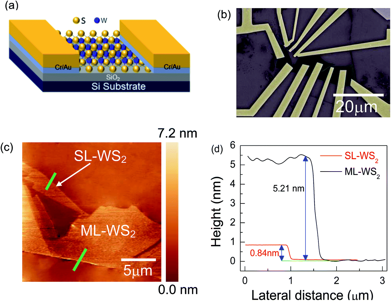
Fig. 1a shows the schematic of a WS2 FET device. Fig. 1b shows the scanning electron microscopic (SEM) image of mechanically exfoliated SL-, ML-WS2 films with Cr/Au electrical contacts. Optical images of SL-, ML-WS2 films with Cr/Au electrical contacts are presented in Fig. S1.† The optical image of WS2 flake on the Si/SiO2 substrate displays different contrasts depending on the thickness of flake (shown in Fig. S1†). The SL-, ML-WS2 flakes were further confirmed by using atomic force microscopy (AFM) and Raman spectra. Fig. 1c represents the surface morphology of the SL-, ML-WS2 films obtained by using AFM. The AFM image was obtained in tapping mode under ambient conditions and the scan area was kept at 20 × 20 μm. The thickness profiles represent that surface of WS2 was uniform with extremely low roughness. The thickness of the SL-WS2 film was measured as 0.84 nm while the thickness of ML-WS2 film was measured as 5.21 nm, which corresponds to seven-layer of WS2 flakes.
 |
| | Fig. 1 (a) Schematic of a WS2 FET. (b) Scanning electron microscopic image of mechanically exfoliated SL-, ML-WS2 films on Si/SiO2 substrate with source–drain contacts. (c) Atomic force microscopy (AFM) image of SL-, ML-WS2 flake. (d) Height profile of the SL-, ML-WS2 along the green line in AFM image. The 0.84 nm thickness indicates one layer of WS2 film. The 5.21 nm thickness indicates seven layers of WS2 film. | |
3.2. Electrical transport measurement in the pristine state
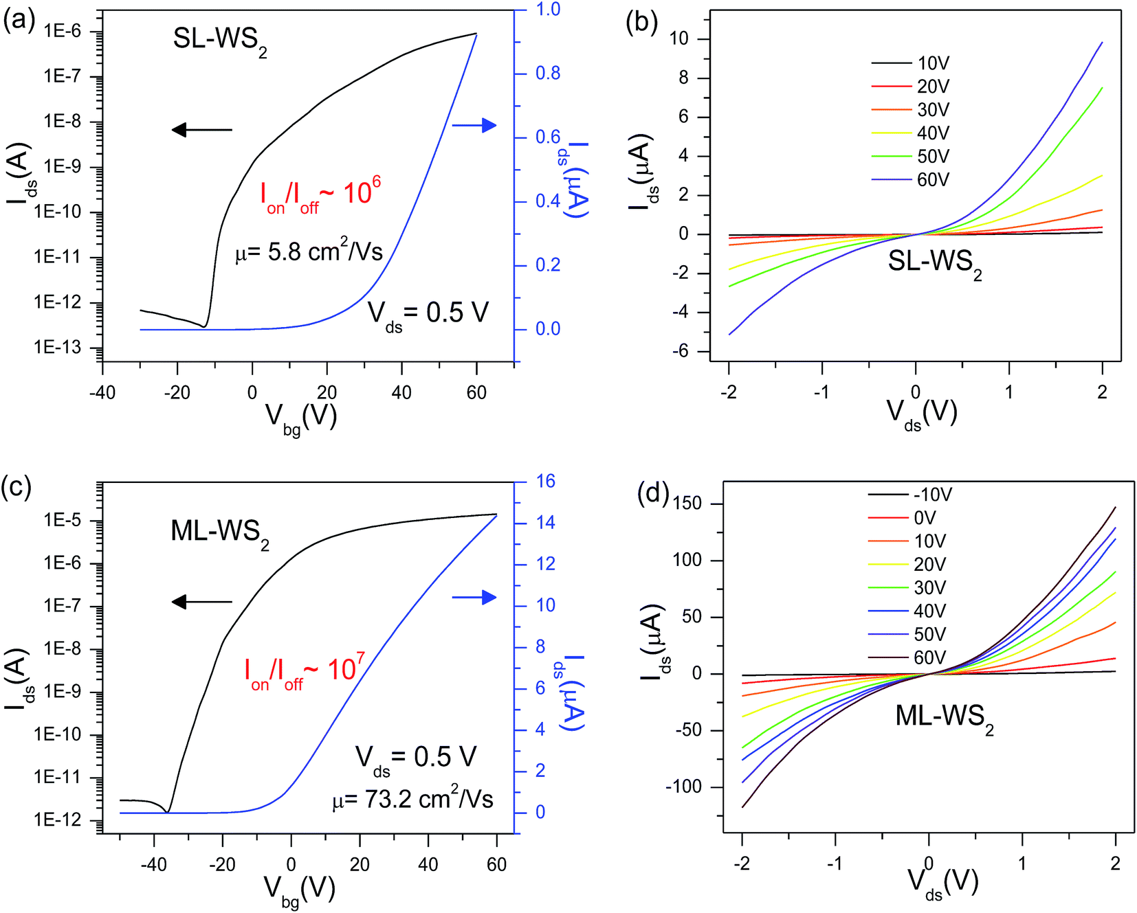
To check the electrical characteristics of the device, electrical transport measurement was investigated at room temperature under vacuum. Fig. 2a shows the transfer characteristics (Ids–Vbg) of the SL-WS2 FET at a fixed source–drain voltage, Vds = 0.5 V. The black curve in the graph is plotted in the logarithmic scale for the Ids–Vbg curve. Output current on/off ratio of the SL-WS2 FET was ≈106, and threshold voltage (Vth) approximately was at 28 V.28,29 The field-effect mobility (μ) of pristine SL-WS2 FET is 5.8 cm2 V−1 s−1. Fig. 2b shows output characteristic (Ids–Vds) curves at various gate voltages ranging from 10 V to 60 V in steps of 10 V for the SL-WS2 FET. The nonlinear behavior in output (Ids–Vds) characteristics represents the existence of Schottky barriers between Cr/Au metal contact and WS2 at the source and drain parts. Similarly, Fig. 2c represents the transfer characteristics (Ids–Vbg) for the ML-WS2 FET. The output current on/off ratio of the ML-WS2 FET was ≈107. Hysteresis in threshold voltage of WS2 FETs was measured around 15–18 V in the pristine samples, less hysteresis in WS2 FETs was measured after KI doping which indicates less charge impurities scattering after the KI doping results are shown Fig. S2.† We have measure three different concentrations (0.01 M, 0.1 M, and 1.0 M) to optimize the controlled doping effect in ML-WS2. Doping is well controlled with optimized time for concentration 0.01 M but with higher concentration like 1.0 M solution. It reaches at saturation point even after 1 min soaking as shown in Fig. S3;† further soaking does not change its characteristics. So different concentration give the similar doping effect but it is time depended. With lower concentration 0.01 M, we have well controlled doping with time. Output (Ids–Vds) characteristic curves at various gate voltages ranging from −10 V to +60 V for the ML-WS2 FET are shown in Fig. 2d.
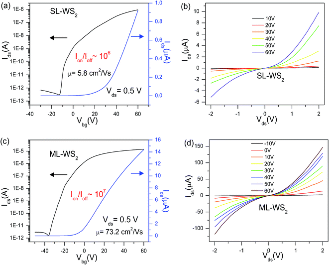 |
| | Fig. 2 (a) Transfer characteristics (Ids–Vbg) of the pristine SL-WS2 FET. On/off ratio of the device is ∼106. (b) Output characteristics (Ids–Vds) of SL-WS2 FET at different back gate voltages ranging from 10 V to 60 V in steps of 10 V. (c) Transfer characteristics (Ids–Vbg) of the pristine ML-WS2 FET. On/off ratio of the device is ∼107. (d) Output characteristics (Ids–Vds) of ML-WS2 FET at different back gate voltages ranging from −10 V to +60 V in steps of 10 V. All measurements were done in vacuum at T = 300 K. | |
3.3. Electrical transport measurement after KI doping
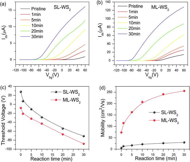
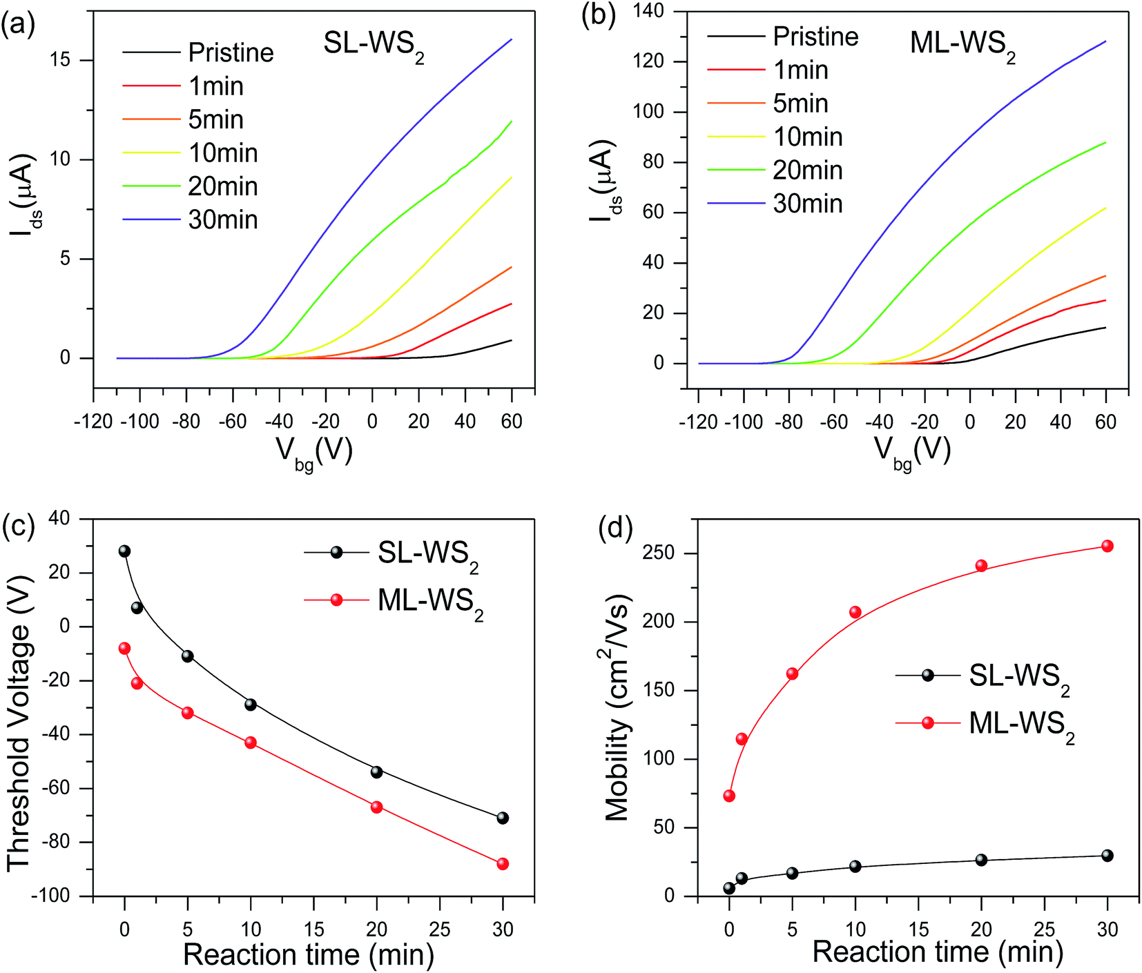
After measuring transport properties at pristine state, we introduced a simple tuning technique to enhance the charge carrier density and mobility. WS2 FETs were treated in KI solution with molar concentration 0.01 M for different periods of time. The effect of KI solution on WS2 FET indicates n-type doping behaviour. Fig. 3a and b show the respective transfer characteristics (Ids–Vbg) of SL-, ML-WS2 FETs after KI doping for different periods. The threshold voltage shifted toward negative gate voltages after KI treatment, which revealed n-type doping for all WS2 FETs. The output current Ids of all WS2 FETs was increased after KI treatment. Fig. 3c represent the change in Vth as a function of treatment time on SL-, ML-WS2 FETs. After the 30 min KI treatment, Vth reached −71, and −88 V for SL-, ML-WS2 FETs respectively. We have also calculated the changes in mobility before and after the chemical doping. Fig. 3d shows the field-effect mobilities of SL-, ML-WS2 FETs at room temperature as a function of reaction time.
 |
| | Fig. 3 Doping effect on WS2 layers by KI treatments. (a) Transfer characteristics (Ids–Vbg) of SL-WS2 FET for different times of treatment. (b) Transfer characteristics (Ids–Vbg) of ML-WS2 FET for different treatment times. (c) Shift of threshold voltage as a function of reaction time by KI for SL-, ML-WS2 FET. (d) Electron mobility as a function of reaction time for SL-, ML-WS2 FET. All measurements were performed in vacuum at T = 300 K. | |
Field-effect mobility was calculated by using the equation  30–32 where L is the channel length, W is the channel width,
  is the slope of transfer characteristic of the device with Vds = 0.5 V, and Cg is the gate capacitance of ∼115 aF μm−2 for the Si/SiO2 substrate.33 The value of
  is obtained by fitting the linear regime of the transfer characteristic curves of WS2 FETs. After 30 min KI treatment, the field-effect mobilities were enhanced to 30 cm2 V−1 s−1 and 255 cm2 V−1 s−1 with on/off ratio ≈107 and ≈108 (shown in Fig. S4†) for SL-, ML-WS2 FETs respectively. While it was measured around 6 cm2 V−1 s−1 and 73 cm2 V−1 s−1 for SL-, ML-WS2 FETs in pristine devices respectively.
The n-type doping effect for WS2 FETs by KI treatment can be described as: tungsten (W) has valence electronic configuration 6s2 5d4 retain an electropositive behavior, presenting capacity to accept electrons. Furthermore, the KI could be dissociated in electropositive K+ (electron acceptor) and electronegative I− (electron donor) ions. When I− atoms are combined in WS2, they occupy the location of sulfur vacancies. Separate impurity energy levels in WS2 would emerge into the conduction band resulting in the bandgap narrowing upon I− ions doping. Thus n-type doping effect in WS2 can attain by the donation of an extra electron from I− ions when they occupy the location of sulfur vacancies.
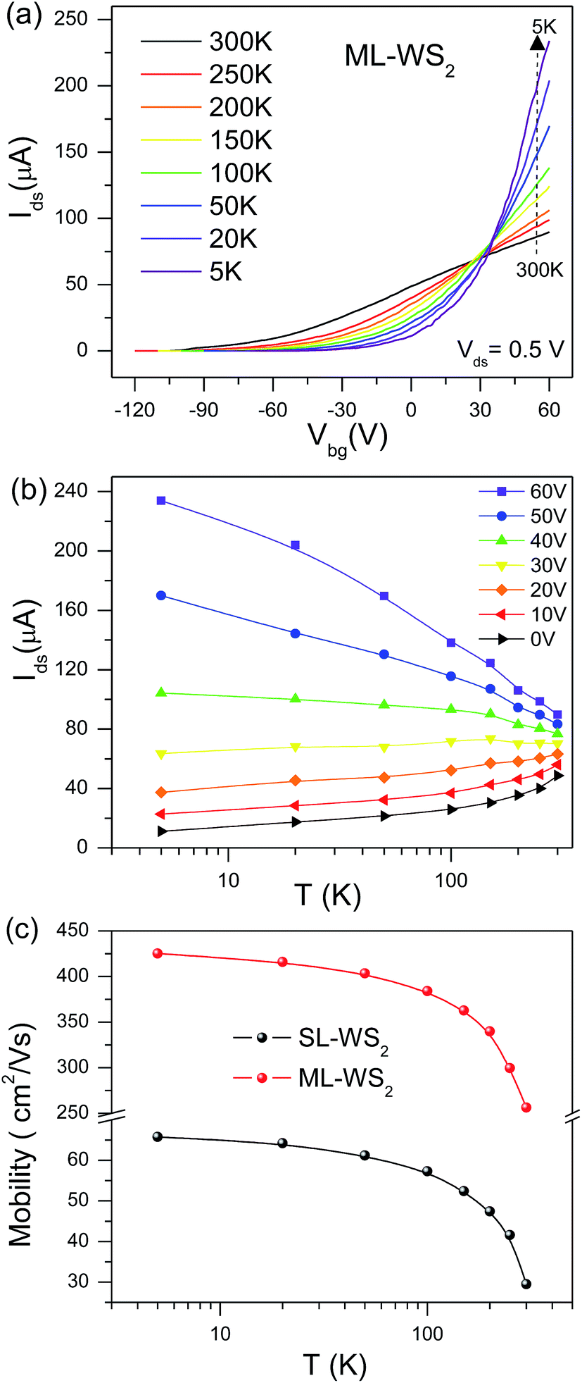
3.4. Temperature-dependent electrical transport properties of ML-WS2 FETs
Temperature-dependent transport properties of ML-WS2 FETs were studied after doping. Fig. 4a represent the transfer characteristics (Ids–Vbg) of the ML-WS2 FET after 30 min chemical doping at fixed Vds = 0.5 V at different temperatures. ML-WS2 FET shows a traditional semiconductor behavior as conductance decreasing with temperature decrease at low gate voltage Vbg < 30 V.34,35 whereas conductance increases as temperature decreased at high gate voltage Vbg > 30 V.36 Semiconductor-to-metal transition at Vbg 30 V suggests that a degenerately doped state is realized in ML-WS2 film.37,38 Fig. 4b shows the temperature dependence of Ids for different values of Vbg. Here, we can clearly understand the critical Vbg of 30 V, at which Ids remains almost independent of temperature. However, the Ids of ML-WS2 FET increases with decreasing temperature for Vbg > 30 V, indicating metallic behavior. For Vbg < 30 V, Ids decreases with decreasing temperature, indicating a semiconducting behavior. Explanations of a similar semiconductor-to-metal transition were described for other transition metal dichalcogenide (TMDCs) materials.39 We have further investigated the electron filed effect mobility of SL-WS2 FET and ML-WS2 on SiO2 at various temperatures. The temperature dependence of μ of SL-, ML-WS2 FETs is compared in Fig. 4c. The electron field-effect motilities of SL-, ML-WS2 FETs on SiO2 were 30 and 255 cm2 V−1 s−1 respectively at T = 300 K and 65 and 425 cm2 V−1 s−1 respectively at T = 5 K.
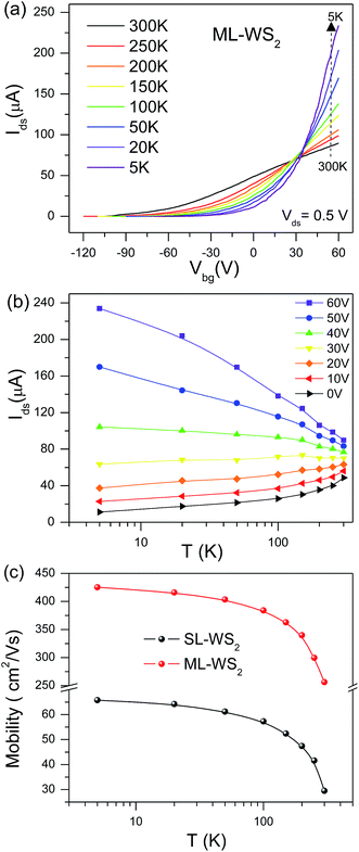 |
| | Fig. 4 (a) Transfer characteristics (Ids–Vbg) of the mechanically exfoliated ML-WS2 FET on SiO2 at different temperatures. (b) Output current as function of temperature for different values of the back-gate voltage. (c) Electron field-effect mobility of SL-, ML-WS2 FETs on SiO2 at various temperatures. | |
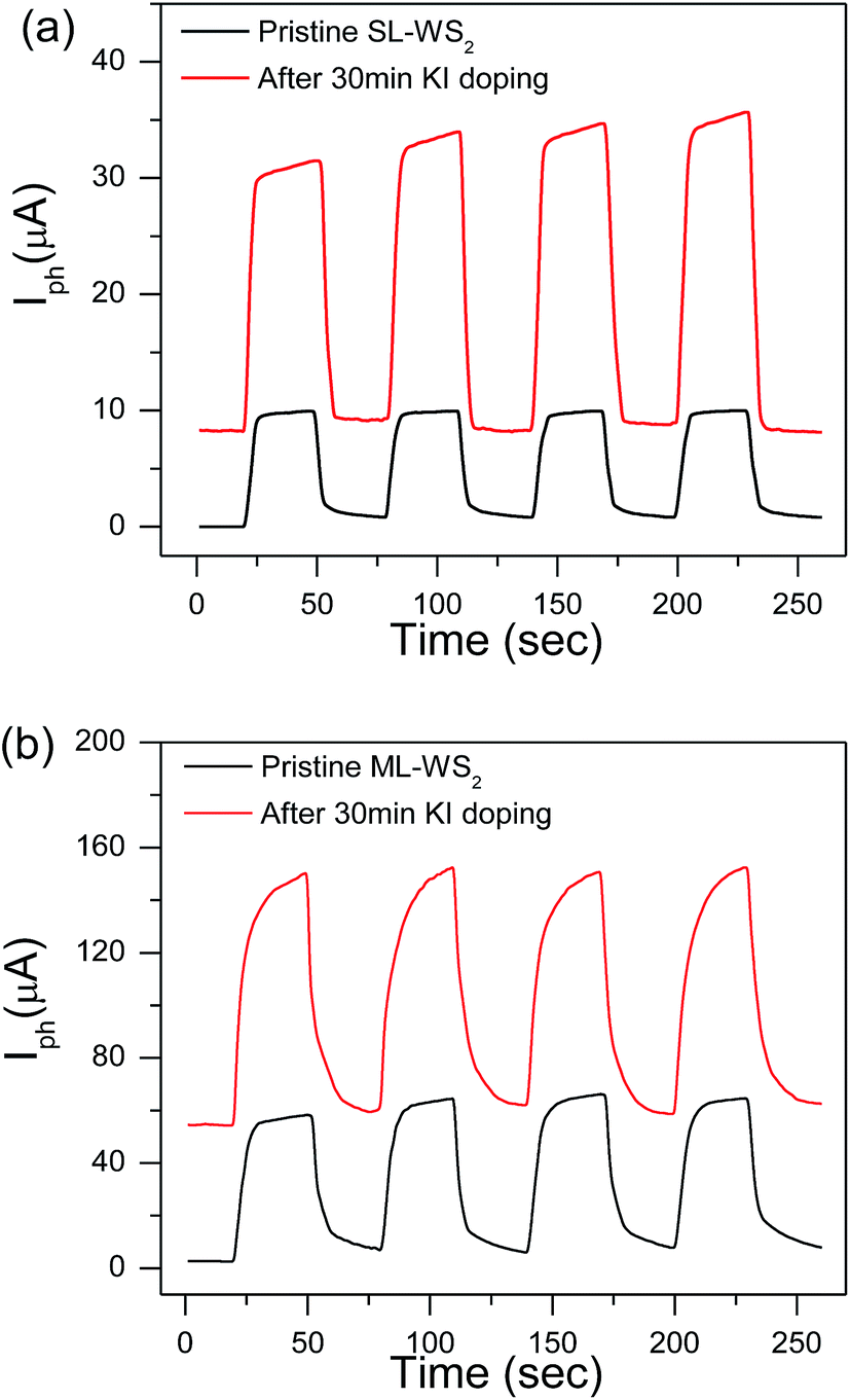
3.5. Photo-electrical measurement under deep-ultraviolet light
Due to a well-developed bandgap, WS2 FETs can also be used as optoelectronic devices. The optoelectronic response of SL-, ML-WS2 FETs in the vacuum by a 220 nm dominant wavelength of deep ultraviolet (DUV) light was measured. A constant bias voltage of 0.5 V was applied between the source and the drain of the WS2 FET, and Ids was monitored for optoelectronic response. Photocurrent (Iph) can be described as difference of Ids with and without light illumination environment.40–42
| Iph = Iilluminated − Idark |
Fig. 5a shows the photocurrent for SL-WS2 FET before and after KI treatment. The photocurrent of SL-WS2 FET was increased about 3 times after chemical doping. The increase in Ids current was due to the improvement in electron mobility by the chemical doping as shown in Fig. 3. A large increase in photocurrent was also observed in ML-WS2 FETs after KI doping as shown in Fig. 5b.
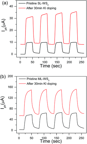 |
| | Fig. 5 Photocurrent of the WS2 FET by 220 nm wavelength dominant DUV illumination before and after KI treatment. A constant bias voltage of 0.5 V was applied between the source and the drain of the WS2 FET. (a) DUV-driven Ids of SL-WS2 FET before (black line) and after (red line) KI treatment. (b) DUV-driven Ids of ML-WS2 FET before (black line) and after (red line) KI treatment. | |
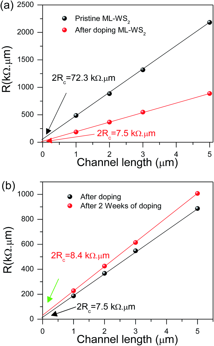
3.6. Contact resistance measurement before and after doping
We have measured the contact resistance of ML-WS2 by using transfer length method (TLM) before and after doping. The specific resistance (ρ = RW) normalized to the sample width was measured due to dependence of resistance (R) on the sample channel width (W). Fig. 6a shows the specific resistance as a function of distance between the contacts. The specific contact resistance (ρc = RcW) of the ML-WS2 device after doping was 3.75 kΩ μm, whereas it was 36.15 kΩ μm for undoped devices. Remarkably decrease in contact resistant after doping leads to increase the drain–source current and improves the device performance. Fig. 6b shows the specific contact resistance of the ML-WS2 film for freshly doped and after 2 weeks to check stability of doping. The specific contact resistance was slightly increased from 3.75 to 4.2 kΩ μm, which confirm that chemical doping is stainable technique.
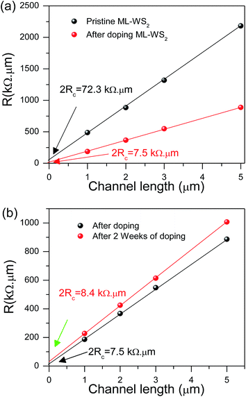 |
| | Fig. 6 Contact resistance measurement by transfer length method. (a) Specific contact resistant (ρc = RcW) for the ML-WS2 device before and after doping. Contact resistant is 3.75 kΩ μm after doping, whereas it was 36.15 kΩ μm before doping. (b) Specific contact resistant (ρc = RcW) for the ML-WS2 after two weeks of doping. | |
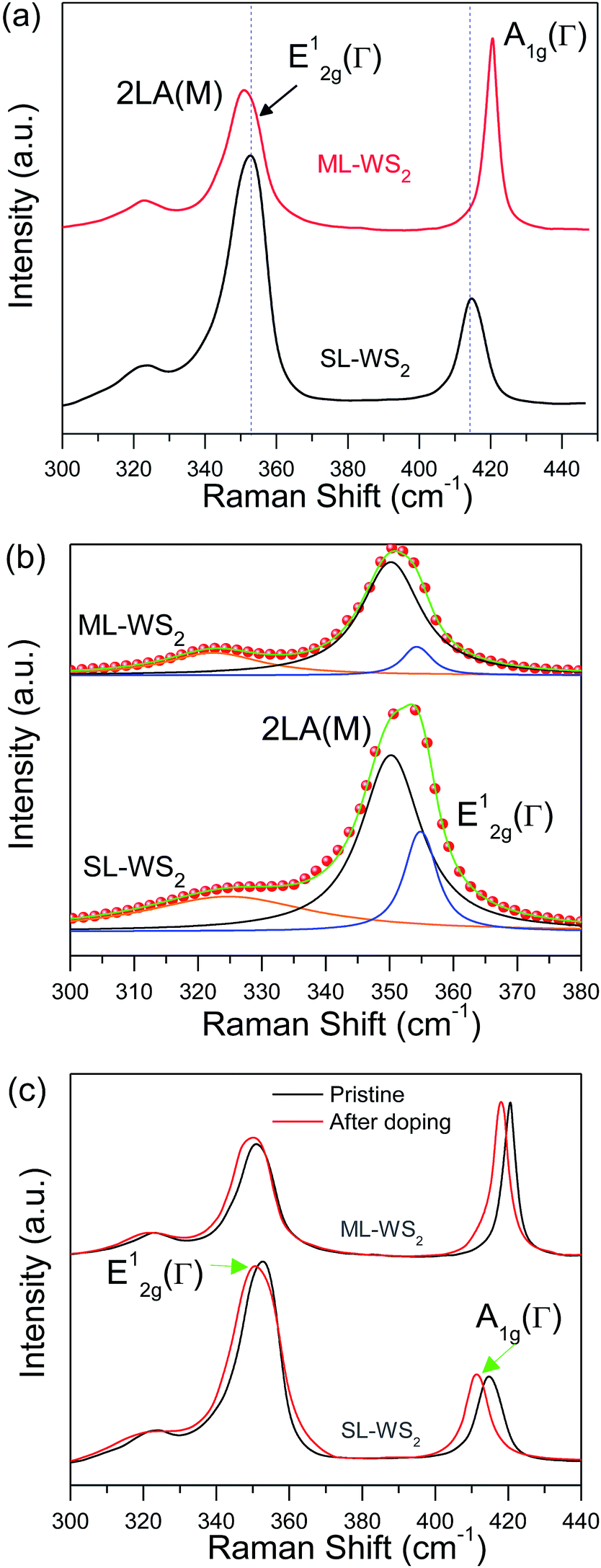
3.7. Raman spectra measurement for different number of WS2 layers
Raman spectroscopy is fast, nondestructive, high resolution technique to study the fundamental properties and structural characterizations of various 2D materials.43 Raman spectroscopy was performed to identify the number of layer and doping effect on SL-WS2, ML-WS2 films. Fig. 7a represents Raman spectra taken for pristine SL-, ML-WS2 films used in our study. Raman spectra of the SL-, ML-WS2 films showed strong signals of in-plane E12g, out-of-plane A1g, and vibration second-order 2LA(M) modes.44 The first-order E12g and A1g optical modes was used to explain the properties of 2D material.45 The frequency difference between A1g and E12g modes was used to explain difference between SL-, ML-WS2.44 The frequency difference between A1g and E12g modes (Δ = A1g − E12g) is about 62.4 cm−1 for SL-WS2, and for ML-WS2 it is Δ = 65.7 cm−1, indicating multiple layers of WS2 film.45 Although the 2LA(M) mode overlapped with the first-order E12g mode, the multi-peak Lorentzian fitting can clarify their individual contributions as seen in Fig. 7b. Chemical doping effect was also examined through Raman spectroscopy. Fig. 7c shows the Raman spectra of the SL-, ML-WS2 films before and after 30 min doping. Red shift was observed in A1g and E12g peaks after doping. A1g peak shifted from 416.3 cm−1 to 412.5 cm−1 for SL-WS2 and from 420.7 cm−1 to 418.2 cm−1 for ML-WS2. Red shift in E12g mode was also observed: 1.9 cm−1 for SL-WS2 and 1.3 cm−1 for ML-WS2. These observations indicate that the A1g vibration mode is more sensitive to doping as compared to E12g. The strong coupling of A1g phonon mode with electron was already reported.32 The A1g Raman peak softens and broadens with the increase of electron doping, whereas the E12g Raman peak weakly depends on the doping. Furthermore, FWHMs of the A1g and E12g peaks were increased for all WS2 films after the 30 min treatment.
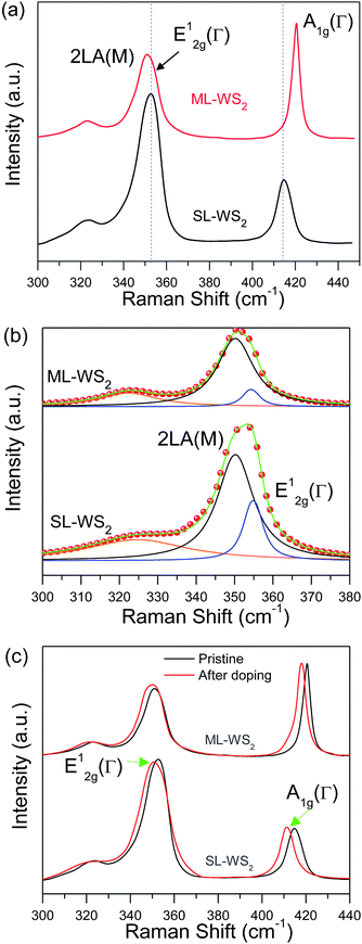 |
| | Fig. 7 Raman spectra for SL-, ML-WS2 films using a laser with 514 nm wavelength. (a) Raman spectra for SL-, ML-WS2 in pristine state. (b) Lorentzian fitting for E2g and 2LA(M) peaks. Red circles represent experimental data, while blue, black, and green lines represent E2g, 2LA(M), and combined peak fitting, respectively. (c) Raman spectra of SL-, ML-WS2 films after 30 min KI treatment. Red shift in A1g and E12g modes was observed after doing. | |
4. Conclusion
In summary, a reliable doping method was developed to considerably enhance the electrical and photoelectric properties of SL-, ML-WS2 FETs. Enhancements in charge carrier mobility and photocurrent response in WS2 FETs after KI doping was confirmed by using electrical transport measurement and Raman spectroscopy. Shift of threshold voltage toward the negative gate voltage and the red shift of the E12g and A1g peaks in the Raman spectra confirm the n-type doping effect in WS2 FETs. Semiconductor-to-metal transition was also observed when Vbg was increased over 30 V. WS2 films show unprecedented high mobility of 255 cm2 V−1 s−1 at room temperature. The on/off ratio of output current is ∼108 at room temperature. The mobility of a ML-WS2 FET was found to be 425 cm2 V−1 s−1 at 5 K. The specific contact resistance was reduced up to 9 times after KI doping. n-Type doping also enhanced the photocurrent in WS2 FETs. Chemical doping exhibited a very stable, effective, and easy-to-apply method to enhance the performance of a WS2 FET.
Acknowledgements
The authors thank the Deanship of Scientific Research, Majmaah University under project No. 37-1-2 for funding this work for financial support. This research was supported by Nano-Material Technology Development Program (2012M3A7B4049888) through the National Research Foundation of Korea (NRF) funded by the Ministry of Science, ICT and Future Planning. This research was also supported by Priority Research Center Program (2010-0020207) and the Basic Science Research Program (2013R1A1A2061396) through NRF funded by the Ministry of Education.
References
- M. Iqbal, A. K. Singh, M. Iqbal and J. Eom, J. Phys.: Condens. Matter, 2012, 24, 335301 CrossRef CAS PubMed.
- A. K. Geim and K. S. Novoselov, Nat. Mater., 2007, 6, 183–191 CrossRef CAS PubMed.
- M. Iqbal, A. K. Singh, M. Iqbal, S. Seo and J. Eom, J. Appl. Phys., 2012, 111, 084307 CrossRef.
- M. Iqbal, S. Siddique, M. Iqbal and J. Eom, J. Mater. Chem. C, 2013, 1, 3078–3083 RSC.
- M. Iqbal, M. F. Khan, M. W. Iqbal and J. Eom, J. Mater. Chem. C, 2014, 2, 5404–5410 RSC.
- C. Zhou, W. Yang and H. Zhu, J. Chem. Phys., 2015, 142, 214704 CrossRef PubMed.
- M. Y. Han, B. Özyilmaz, Y. Zhang and P. Kim, Phys. Rev. Lett., 2007, 98, 206805 CrossRef PubMed.
- A. J. Samuels and J. D. Carey, ACS Nano, 2013, 7, 2790–2799 CrossRef CAS PubMed.
- J. B. Oostinga, H. B. Heersche, X. Liu, A. F. Morpurgo and L. M. Vandersypen, Nat. Mater., 2008, 7, 151–157 CrossRef CAS PubMed.
- X. Li, X. Wang, L. Zhang, S. Lee and H. Dai, Science, 2008, 319, 1229–1232 CrossRef CAS PubMed.
- T. Georgiou, R. Jalil, B. D. Belle, L. Britnell, R. V. Gorbachev, S. V. Morozov, Y.-J. Kim, A. Gholinia, S. J. Haigh and O. Makarovsky, Nat. Nanotechnol., 2013, 8, 100–103 CrossRef CAS PubMed.
- W. Zhao, Z. Ghorannevis, L. Chu, M. Toh, C. Kloc, P.-H. Tan and G. Eda, ACS Nano, 2012, 7, 791–797 CrossRef PubMed.
- N. Peimyoo, W. Yang, J. Shang, X. Shen, Y. Wang and T. Yu, ACS Nano, 2014, 8, 11320–11329 CrossRef CAS PubMed.
- T. Georgiou, H. Yang, R. Jalil, J. Chapman, K. S. Novoselov and A. Mishchenko, Dalton Trans., 2014, 43, 10388–10391 RSC.
- S. Jo, N. Ubrig, H. Berger, A. B. Kuzmenko and A. F. Morpurgo, Nano Lett., 2014, 14, 2019–2025 CrossRef CAS PubMed.
- W. S. Hwang, M. Remskar, R. Yan, V. Protasenko, K. Tahy, S. D. Chae, P. Zhao, A. Konar, H. G. Xing and A. Seabaugh, Appl. Phys. Lett., 2012, 101, 013107 CrossRef.
- N. Perea-López, A. L. Elías, A. Berkdemir, A. Castro-Beltran, H. R. Gutiérrez, S. Feng, R. Lv, T. Hayashi, F. López-Urías and S. Ghosh, Adv. Funct. Mater., 2013, 23, 5511–5517 CrossRef.
- N. Huo, S. Yang, Z. Wei, S.-S. Li, J.-B. Xia and J. Li, Sci. Rep., 2014, 4, 5209 CAS.
- S. Bertolazzi, D. Krasnozhon and A. Kis, ACS Nano, 2013, 7, 3246–3252 CrossRef CAS PubMed.
- D. Ovchinnikov, A. Allain, Y.-S. Huang, D. Dumcenco and A. Kis, ACS Nano, 2014, 8, 8174–8181 CrossRef CAS PubMed.
- F. Withers, T. H. Bointon, D. C. Hudson, M. F. Craciun and S. Russo, Sci. Rep., 2014, 4, 4967 CAS.
- D. J. Late, B. Liu, H. R. Matte, V. P. Dravid and C. Rao, ACS Nano, 2012, 6, 5635–5641 CrossRef CAS PubMed.
- W. Liu, J. Kang, D. Sarkar, Y. Khatami, D. Jena and K. Banerjee, Nano Lett., 2013, 13, 1983–1990 CrossRef CAS PubMed.
- S. Das, H.-Y. Chen, A. V. Penumatcha and J. Appenzeller, Nano Lett., 2012, 13, 100–105 CrossRef PubMed.
- M. P. Levendorf, C.-J. Kim, L. Brown, P. Y. Huang, R. W. Havener, D. A. Muller and J. Park, Nature, 2012, 488, 627–632 CrossRef CAS PubMed.
- P. Yen, Y. Huang and K. Tiong, J. Phys.: Condens. Matter, 2004, 16, 2171 CrossRef CAS.
- S. Mouri, Y. Miyauchi and K. Matsuda, Nano Lett., 2013, 13, 5944–5948 CrossRef CAS PubMed.
- D. Kiriya, M. Tosun, P. Zhao, J. S. Kang and A. Javey, J. Am. Chem. Soc., 2014, 136, 7853–7856 CrossRef CAS PubMed.
- M. W. Iqbal, M. Z. Iqbal, M. F. Khan, M. A. Shehzad, Y. Seo and J. Eom, Nanoscale, 2015, 7, 747–757 RSC.
- Y. Zhan, Z. Liu, S. Najmaei, P. M. Ajayan and J. Lou, Small, 2012, 8, 966–971 CrossRef CAS PubMed.
- Y.-H. Lee, L. Yu, H. Wang, W. Fang, X. Ling, Y. Shi, C.-T. Lin, J.-K. Huang, M.-T. Chang and C.-S. Chang, Nano Lett., 2013, 13, 1852–1857 CrossRef CAS PubMed.
- J. D. Lin, C. Han, F. Wang, R. Wang, D. Xiang, S. Qin, X.-A. Zhang, L. Wang, H. Zhang and A. T. S. Wee, ACS Nano, 2014, 8, 5323–5329 CrossRef CAS PubMed.
- M. W. Iqbal, M. Z. Iqbal, X. Jin, J. Eom and C. Hwang, J. Mater. Chem. C, 2014, 2, 7776–7784 RSC.
- S. Kim, A. Konar, W.-S. Hwang, J. H. Lee, J. Lee, J. Yang, C. Jung, H. Kim, J.-B. Yoo and J.-Y. Choi, Nat. Commun., 2012, 3, 1011 CrossRef PubMed.
- S. El-Mahalawy and B. Evans, Phys. Status Solidi A, 1977, 79, 713–722 CrossRef CAS.
- V. Podzorov, M. Gershenson, C. Kloc, R. Zeis and E. Bucher, Appl. Phys. Lett., 2004, 84, 3301–3303 CrossRef CAS.
- B. Chamlagain, Q. Li, N. J. Ghimire, H.-J. Chuang, M. M. Perera, H. Tu, Y. Xu, M. Pan, D. Xaio and J. Yan, ACS Nano, 2014, 8, 5079–5088 CrossRef CAS PubMed.
- B. Radisavljevic and A. Kis, Nat. Mater., 2013, 12, 815–820 CrossRef CAS PubMed.
- B. Chakraborty, A. Bera, D. Muthu, S. Bhowmick, U. V. Waghmare and A. Sood, Phys. Rev. B: Condens. Matter Mater. Phys., 2012, 85, 161403 CrossRef.
- M. Buscema, D. J. Groenendijk, S. I. Blanter, G. A. Steele, H. S. van der Zant and A. Castellanos-Gomez, Nano Lett., 2014, 14, 3347–3352 CrossRef CAS PubMed.
- O. Lopez-Sanchez, D. Lembke, M. Kayci, A. Radenovic and A. Kis, Nat. Nanotechnol., 2013, 8, 497–501 CrossRef CAS PubMed.
- C. Lan, C. Li, Y. Yin and Y. Liu, Nanoscale, 2015, 7, 5974–5980 RSC.
- M. W. Iqbal, M. Z. Iqbal, X. Jin, C. Hwang and J. Eom, ACS Appl. Mater. Interfaces, 2014, 6, 4207–4213 CAS.
- A. Berkdemir, H. R. Gutiérrez, A. R. Botello-Méndez, N. Perea-López, A. L. Elías, C.-I. Chia, B. Wang, V. H. Crespi, F. López-Urías and J.-C. Charlier, Sci. Rep., 2013, 3, 1755 Search PubMed.
- H. Zeng, G.-B. Liu, J. Dai, Y. Yan, B. Zhu, R. He, L. Xie, S. Xu, X. Chen and W. Yao, Sci. Rep., 2013, 3, 1608 Search PubMed.
Footnote |
| † Electronic supplementary information (ESI) available. See DOI: 10.1039/c6ra02390h |
|
| This journal is © The Royal Society of Chemistry 2016 |

 30–32 where L is the channel length, W is the channel width,
  is the slope of transfer characteristic of the device with Vds = 0.5 V, and Cg is the gate capacitance of ∼115 aF μm−2 for the Si/SiO2 substrate.33 The value of
  is obtained by fitting the linear regime of the transfer characteristic curves of WS2 FETs. After 30 min KI treatment, the field-effect mobilities were enhanced to 30 cm2 V−1 s−1 and 255 cm2 V−1 s−1 with on/off ratio ≈107 and ≈108 (shown in Fig. S4†) for SL-, ML-WS2 FETs respectively. While it was measured around 6 cm2 V−1 s−1 and 73 cm2 V−1 s−1 for SL-, ML-WS2 FETs in pristine devices respectively.