
N- and p-type doping of antimonene†
Meiqiu Xie,
Shengli Zhang‡
,
Bo Cai,
Yousheng Zou and
Haibo Zeng*
Institute of Optoelectronics and Nanomaterials, Jiangsu Key Laboratory of Advanced Micro & Nano Materials and Technology, College of Materials Science and Engineering, Nanjing University of Science and Technology, Nanjing 210094, China. E-mail: zeng.haibo@njust.edu.cn
First published on 20th January 2016
Abstract
Antimonene, monolayer antimony, was recently predicted to be a two-dimensional (2D) semiconductor with a blue photoresponse. N- and p-type doping of this material is essential for its future application in optoelectronic devices, but has not yet been carried out. Here, we introduce tetrathiafulvalene (TTF) and tetracyanoquinodimethane (TCNQ) as electron and hole dopants to attain n- and p-type antimonene semiconductors. Then, the electronic properties of the chemically doped antimonene are investigated based on comprehensive first-principles calculations. Through TTF modified antimonene, we acquire an n-type semiconductor with a deep donor state of 0.73 eV. Importantly, through TCNQ functionalized antimonene, a p-type semiconductor is achieved with a shallow acceptor state of 0.27 eV. Moreover, the co-adsorption of TTF and TCNQ on antimonene can significantly decrease the band-gaps to 0.15 and 0.12 eV in the one- and two-side configurations, respectively, exhibiting n-type semiconductance with shallow donor states. Such n- and p-type antimonene semiconductors may widen the application of two-dimensional semiconductors in electronics and optoelectronics.
1. Introduction
Two-dimensional (2D) crystals have emerged as a novel class of materials with a wide range of extraordinary electronic and optoelectronic properties.1 For example, graphene,2,3 transition metal dichalcogenides (TMDCs),4,5 and phosphorene6,7 have rapidly become fascinating building blocks for photonic and optoelectronic applications. Currently, much attention is being paid to different kinds of photodetection platforms.8–11 Graphene-based photodetectors possess broadband and ultrafast responses, but undergo short photogenerated carrier lifetimes because of lacking an intrinsic bandgap.9,10 Therefore, materials scientists and chemists have committed themselves to exploring photosensitive TMDCs such as monolayer MoS2 field effect transistors (FETs), which are extensively studied 2D semiconductors with suitable bandgap.12,13 However, limitations exist with these MoS2 devices such as a low carrier mobility of 200 cm2 V−1 s−1, improvable up to 500 cm2 V−1 s−1,12 which is still lower than that of graphene. Thus, there is an urgency to search for new 2D materials.Recently, phosphorene has been synthesized through mechanically exfoliating black phosphorus crystals14–20 and used to fabricate the channel material in a FET with a superior mobility of up to 1000 cm2 V−1 s−1.21–23 Quite recently, motivated by such advantages on phosphorene, the elemental materials arsenene and antimonene of group-V, regarded as being chemically similar to phosphorene, have also been studied.24–29 For example, Zhang et al.24 theoretically reported two new atomically thin 2D semiconductors, namely arsenene (As monolayer) and antimonene (Sb monolayer), with high stability and wide band-gap. Therefore, a honeycomb of single-layer antimony is expected to possess comparable or even better properties than phosphorene.
In 2014, it was shown that a 2D monolayer semiconductor with an adsorbing molecule can generate effective n-doping, as well as construct a p–n junction with an excellent performance.30 Therefore, chemical doping is an effective approach to obtain an in-plane 2D p–n junction. Remarkably, in comparison with routine doping methods,31 chemical doping will preserve the structural integrity and excellent properties of 2D materials. Meanwhile in recent years, several theoretical and experimental studies have alternatively put forward n- or p-doping of 2D materials utilizing charge transfer using chemical dopants. Indeed, many researchers have theoretically predicted that modifying a substrate with organic molecules, such as tetracyanoquinodimethane (TCNQ), tetracyanoethylene (TCNE), tetrathiafulvalene (TTF) and benzyl viologen (BV), etc., can turn the substrate into a p- or n-type semiconductor.32–35 Until now, however, few theoretical reports have been implemented to understand, control and modulate the electronic properties of monolayer antimonene through chemical modifications.
In this work, a theoretical model of antimonene is developed to analyze the chemical doping effects of TTF and TCNQ using comprehensive first-principles calculations. We investigate the chemical doping of single-atom-thick antimonene by using TTF and TCNQ molecules, and achieve n- or p-type monolayer antimonene semiconductors. Formation of the n- or p-type semiconductor is crucial in becoming p–n junctions which determines the photoresponse in antimonene photodetectors. Moreover, the doping effect can be ascribed to the influence of the electron donor or acceptor on antimonene during the charge state conversion, as shown in Fig. 1(a). It is found that the doping of these two organic molecules results in a sharp decrease in the bandgap, and converts antimonene into an n- or p-type semiconductor corresponding to a deep or shallow energy level, respectively. In addition, the co-adsorption of TTF and TCNQ on antimonene can also achieve an n-type semiconductor with a shallow energy level.
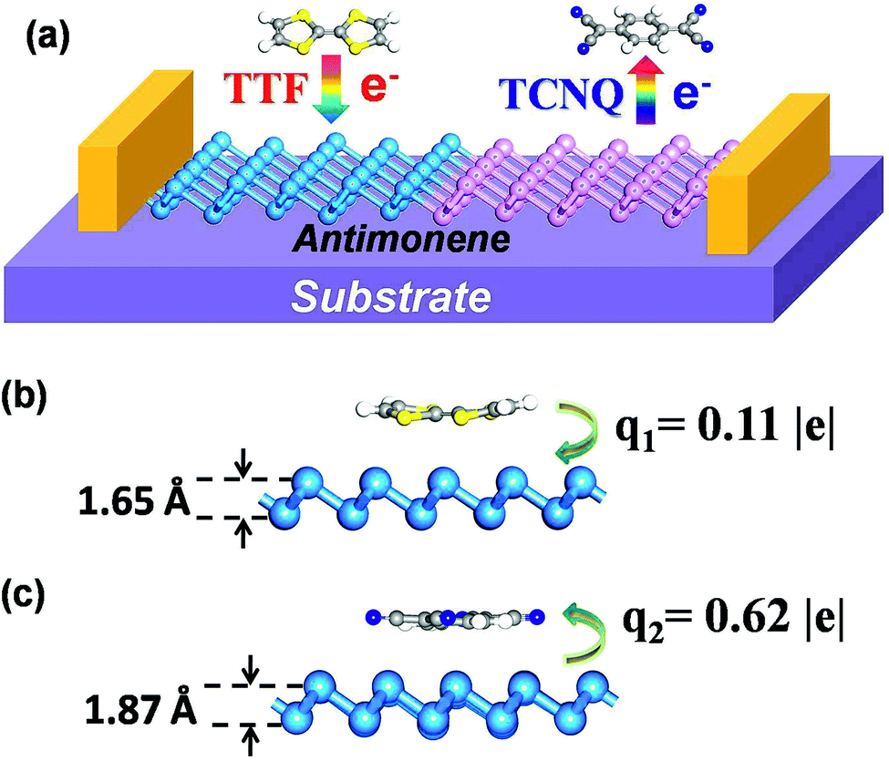 | ||
| Fig. 1 (a) Schematic illustration of the antimonene device used for TTF and TCNQ surface electron and hole transfer doping studies. The lowest-energy configurations of (b) TTF/antimonene and (c) TCNQ/antimonene are shown in side view. Additionally, the charge transfer between the molecules and antimonene, and the twisting distance of the antimonene nanosheet are displayed. | ||
2. Computational details
Plane-wave density functional theory (DFT) calculations were employed by using the Cambridge sequential total energy package (CASTEP) code.36 The generalized gradient approximation (GGA) of Perdew, Burke, and Ernzerhof (PBE) for the exchange–correlation functional was used,37 as well as the norm-conserving pseudopotentials38 being depicted in the core valence interactions (valence electrons included in this study for distinct atoms are Sb 5s2 5p3, O 2s2 2p4, S 3s2 3p4, C 2s2 2p2 and N 2s2 2p3). For introducing the van der Waals (vdW) interactions, we adopted the semiempirical dispersion corrections using the DFT-D approach with the Grimme scheme.39 During the geometry optimization, the models were relaxed until the total energy tolerances and forces were less than 5 × 10⁻⁶ eV per atom and 0.01 eV Å−1, respectively. The plane wave basis set with a cutoff energy of 500 eV was adopted. A larger grid of 5 × 5 × 1 was sampled for band structure and scanning tunneling microscopy (STM) simulations.On the basis of our current understanding, the buckled system, Fig. S1,† is the most stable configuration.24 The relaxed lattice constants for antimonene are a = b = 3.94 Å. To investigate the chemical doping of 2D antimonene using TTF and TCNQ molecules, a 5 × 5 × 1 antimonene supercell including 50 atoms is applied. The nearest distance between two chemical molecules (i.e., TTF and TCNQ) in adjoining supercells is ∼10 Å, and a bigger vacuum layer of 20 Å is adopted to forbid the interaction between two adjoining unit cells. In order to estimate the most favorable configurations of the chemical doping in antimonene, the adsorption energy per molecule is delineated as:
| Ea = Emolecule/antimonene − Eantimonene − Emolecule |
3. Results and discussion
The structure of monolayer antimonene is presented in Fig. S1† from three perspectives. Each unit cell of antimonene is composed of two Sb atoms, which are all bonded with three adjacent Sb atoms. The buckling height and angle of the buckled antimonene are measured to be 1.55 Å and 91.31°,24 respectively. So the two neighboring bond connected Sb are regarded as different atoms, and we label them T1 and T2, as presented in Fig. S1.† On the other hand, due to the highly symmetrical geometries of our considered organic molecules (TTF and TCNQ), four chemical doping positions were chosen for each molecule (Fig. S1, S2(a), and S3(a)†): the top sites 1 and 2 (T1 and T2), the center of a Sb–Sb bond (B), and the central hollow ring (H). For each of these sites, we squared up the orientations of the two molecules, respectively, i.e., the long axis of the molecules being along the armchair- or zigzag-direction in TCNQ/antimonene. However, for TTF/antimonene, except for the above-displayed two situations, an extra two situations exist such as the long axis of TTF deviating 30° away from the positive direction of the x- or y-axis. The doped molecules of TCNQ and TTF were firstly set parallel to the monolayer antimonene.The relaxed structures of TTF/antimonene and TCNQ/antimonene, together with the relative total energy of the lowest-energy configuration are shown in Fig. S2(b) and S3(b).† Following this, we only include further detailed discussion on the most stable modified antimonene monolayers with the side views which can be seen in Fig. 1(b) and (c) (the top views are shown in Fig. S2(b) and S3(b)†). For the nucleophilic molecule TTF (Fig. 1(b)) the most favorable geometry is the T2 site, with its long axis deviating 30° away from the positive direction of the x-axis in the unit cell, and the perpendicular distance between TTF and antimonene is ∼3.20 Å. In addition, the adsorption energy of TTF/antimonene is −0.61 eV, implying an interaction between TTF and antimonene, which leads to a serious twisting of TTF deviating from the flat plane of the TTF molecule, and the maximal variation (corresponding to the original flat-type TTF molecule) of the atoms in the TTF molecule is 0.76 Å. Meanwhile, the single-layer antimonene is negligibly tumbled 0.09 Å from the origin plane of antimonene (with an origin height of 1.55 Å). The lowest-energy functionalized structure for the electrophilic molecule TCNQ is also the T2 site, with its long axis along the x-direction of the monolayer antimonene, and the separation between the organic molecule and monolayer antimonene is ∼3.15 Å, as presented in Fig. 1(c). Furthermore, owing to the adsorption of TCNQ (adsorption energy reaches −1.70 eV), both TCNQ and the single-layer antimonene are seriously deformed. For the relaxed TCNQ/antimonene model, the TCNQ molecule and monolayer antimonene are 0.31 Å and 0.32 Å away from the original flat plane of the TCNQ molecule and antimonene (with an origin height of 1.55 Å), respectively.
In order to inspect the influence of non-covalent molecular doping on the electronic properties of antimonene, the electronic band structures of free-standing and functionalized antimonene were computed (in Fig. 2(a)–(c)). It is obvious that the flat energy levels emerge above and below the Fermi level (EF) corresponding to the TCNQ and TTF adsorbed antimonene, respectively. Herein, we designate these two bands as the acceptor and donor energy levels in the TCNQ/antimonene, and TTF/antimonene configurations, respectively. Evidently, the isolated antimonene is a semiconductor with a bandgap of 1.77 eV, as shown in Fig. 2(a). In comparison with pristine antimonene, the band gaps of the doped systems are dramatically decreased by 0.73 eV and 0.27 eV for TTF/antimonene and TCNQ/antimonene, respectively. As we all know, Kohn–Sham DFT often underestimates bandgaps, so we recomputed the band structure of freestanding antimonene and TCNQ/antimonene, resulting in 2.62 eV and 0.66 eV, using the Heyd–Scuseria–Ernzerhof (HSE06)40 method as shown in Fig. S5.† Herein, for chemically doped systems, we take TCNQ/antimonene as an example. The VBM and CBM positions with respect to the high symmetry point are in good accordance with the PBE level. On account of the interaction between the organic molecule (TTF or TCNQ) and single-layer antimonene, the renewed band structure of the doped samples can be treated as a recombination after adsorption of the molecules onto antimonene, besides the recombination of the energy levels creates the decreased band gaps.
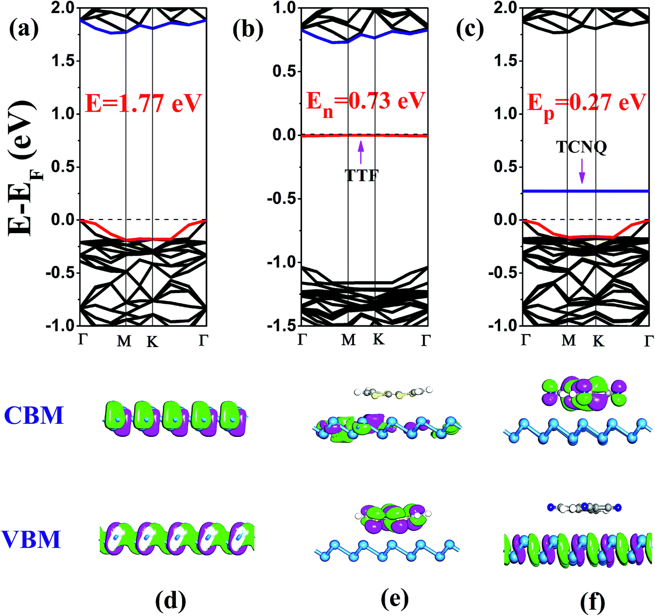 | ||
| Fig. 2 Electronic band structures and the side views of partial charge density for CBM and VBM of (a and d) pristine antimonene, (b and e) TTF/antimonene, and (c and f) TCNQ/antimonene, respectively. Additionally, the red and blue lines indicate the located bands of the valence band maximum (VBM) and the conduction band minimum (CBM), respectively. The horizontal dotted lines indicate the Fermi level. | ||
The above-mentioned new energy levels (acceptor and donor energy levels) in the molecule-modified antimonene are quite different to those in pristine antimonene. Here, we define the concept En as the new bandgap between the highest occupied molecular band (HOMO) of TTF and the conduction band minimum (CBM) of monolayer antimonene after doping. Similarly, the new bandgap Ep stands for the lowest unoccupied molecular band (LUMO) of TCNQ and the valence band maximum (VBM) of antimonene after doping. It is well known that a p- or n-type semiconductor determines the Fermi level EF, which moves down or up after doping. For the TTF doped configuration, the Fermi level EF moves up compared to the isolated antimonene, as can be seen by comparing Fig. 2(a) with 2(b). Actually, EF is close to CBM which stems from the monolayer antimonene (analyzed later) rather than VBM, so it is an n-type semiconductor. However, according to the band gap of 0.73 eV (En = 0.73 eV), it is geared to a deep gap level. Actually, only 0.11|e| transforms from the organic molecule TTF to the antimonene nanosheet, revealed by the Hirshfeld charge analysis. It is illustrated that TTF as an electron dopant can be used to attain n-type antimonene. In comparison with the electrophilic TCNQ molecule doped sample, Fig. 2(c), EF decreases and definitely approximates VBM, together with the calculated Ep being small with a band gap of 0.27 eV, implying that it creates a shallow gap level, so it is a typical p-type semiconductor. Similarly, there is an appreciable 0.62|e| charge transfer from antimonene to TCNQ, calculated using Hirshfeld charge analysis. Thus, it is evident that TCNQ as a hole dopant can be used to achieve a typical p-type antimonene.
To verify the above conclusions about TTF/antimonene and TCNQ/antimonene, side views of the partial charge density of the CBM and VBM for these two structures are shown in Fig. 2(d)–(f). The top views of the favorable samples are shown in the ESI Fig. S4.† Comparing Fig. 2(d) with 2(e), both the CBM and VBM of the pristine antimonene sheet are combinations of mainly 5p orbitals, but the VBM is coupled with small amounts of 5s states. For the electron-donating sample, the presented CBM is indeed due to monolayer antimonene, and the VBM, i.e., donor energy level here, is attributed to the highest occupied molecular orbital (HOMO) of TTF. Fig. S6(a)† presents that the new energy level below EF, i.e., the VBM of TTF/antimonene, is indeed contributed by the TTF molecule (mainly p orbital, i.e., the contribution set of each atom (p-orbital) in TTF). The result is in satisfactory accordance with the analysis of the partial charge density and band structure in TTF/antimonene. Nevertheless, as shown in Fig. 2(f), for the electron-withdrawing molecule doped antimonene, the VBM of this system comes from single-layer antimonene, and the CBM, that is the acceptor energy level herein, originates from the lowest unoccupied molecular orbital (LUMO) of TCNQ. Meanwhile, the introduced new energy level above EF, i.e., the CBM of TCNQ/antimonene, indeed stemmed from the TCNQ molecule (mainly p orbital, i.e., the contribution set of every atom (p-orbital) in TCNQ), as presented in Fig. S6(b).† This is in good agreement with the conclusion that an n-type semiconductor can be procured through encapsulating nucleophilic molecules into antimonene, and electrophilic molecules doped into antimonene can create a typical p-type semiconductor.
STM has been used to explore the atomic-realm of surfaces in real space, observing surface defects, surface reconstruction, the shape and position of surface adsorbents, and surface reconstruction caused by the adsorbent. The STM images of pristine antimonene, TTF/antimonene, and TCNQ/antimonene were simulated at +0.6 V and −0.6 V bias (Fig. 3). The negative and positive biases of STM correspond to the VBM and CBM of the structure, respectively. As shown in Fig. 3(a), the STM image is in good accordance with the CBM and VBM in pristine antimonene. Now, through comparison of Fig. 3(b) with 3(c), it is easy to observe that the STM images of TTF-modified antimonene (at positive bias (+0.6 V)) and TCNQ-modified antimonene (at negative bias (−0.6 V)) show buckling of the antimonene. Meanwhile, TTF-modified antimonene (−0.6 V) is ascribed to the electron-donating molecule (TTF), while TCNQ-modified antimonene (+0.6 V) is owing to electron accepting molecule (TCNQ). These conclusions are all consistent with the above analysis. This will give information to future experiments about the chemical doping of antimonene.
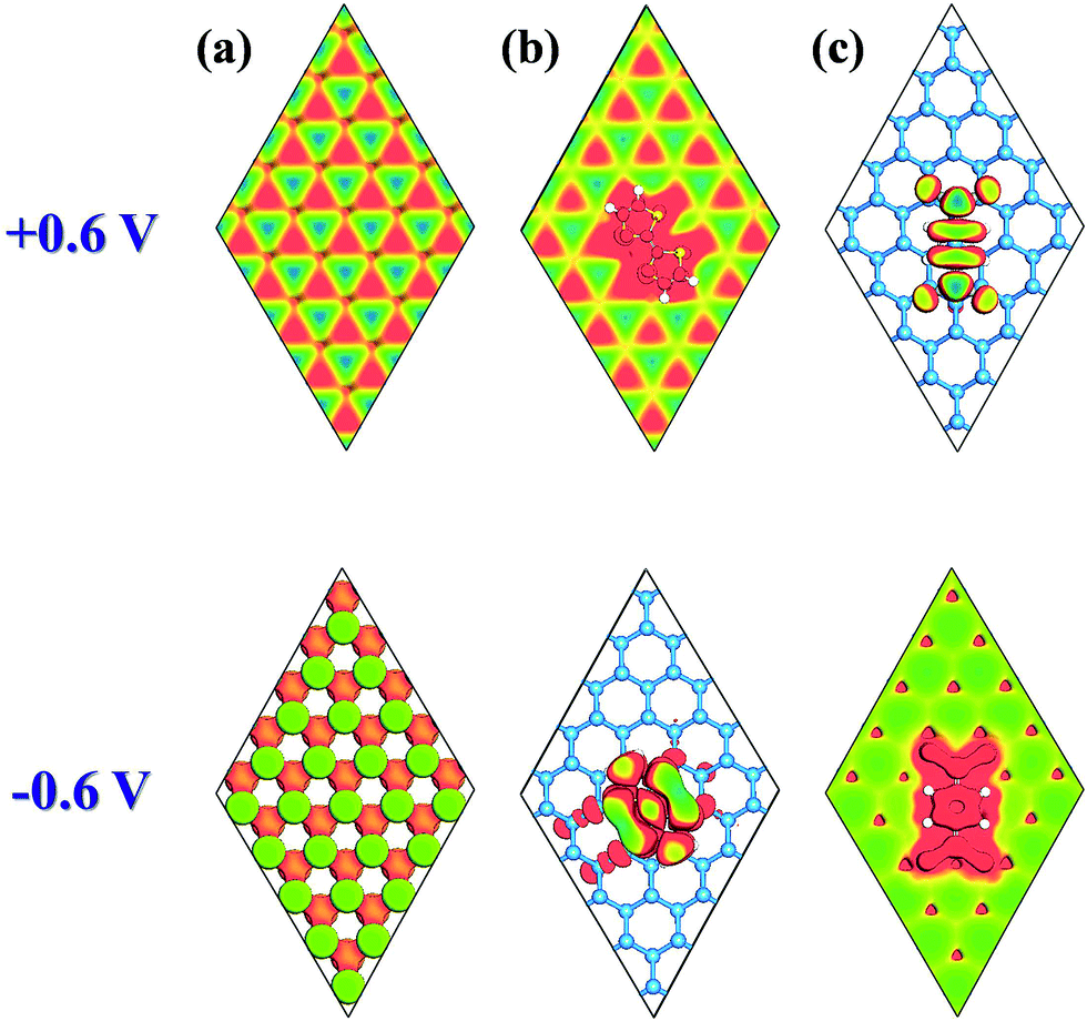 | ||
| Fig. 3 Simulated STM images (+0.6 and −0.6 V) for (a) pristine antimonene, (b) TTF/antimonene, and (c) TCNQ/antimonene, shown by top views. | ||
Based on the above-displayed behaviour of a single type of molecule (TTF or TCNQ) adsorbed on antimonene, how about the co-adsorption of TTF and TCNQ on antimonene? In order to answer this question, the co-adsorption of TTF and TCNQ on antimonene was studied. Considering the lowest-energy configurations of TTF/antimonene and TCNQ/antimonene, we exhibit these two structures using the 8 × 8 supercell antimonene. The optimized configurations and band structures for co-adsorbed TTF and TCNQ on one-side (a) and two-sides (b) of antimonene are displayed in Fig. S6† and 4, respectively (for detailed captions refer to the ESI†).
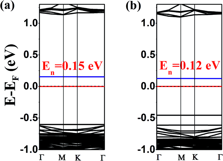 | ||
| Fig. 4 Electronic band structures for the co-adsorption of TTF and TCNQ on (a) one-side and (b) two-sides of antimonene. Additionally, the red and blue lines indicate the located bands of the VBM and CBM, respectively. The horizontal dotted line indicates the Fermi level. | ||
The calculated results show that both the one- and two-side configurations for the co-adsorption of TTF and TCNQ on antimonene are n-type semiconductors. The bandgaps are 0.15 eV and 0.12 eV corresponding to the one-side and two-side configurations, respectively. Both of them are less than the single molecule [TTF (0.73 eV) or TCNQ (0.27 eV)] adsorbed on the substrate. Meanwhile, we find that both of these two systems have shallow gap levels. Actually, for the one-side structure, the charge 0.29|e| (larger than 0.11|e|, compared with the single adsorbed TTF/antimonene) transforms from TTF to the antimonene nanosheet. Simultaneously, 0.42|e| (smaller than 0.62|e|, compared with the single adsorbed TCNQ/antimonene) transfers from the antimonene nanosheet to TCNQ, revealed using Hirshfeld charge analysis. The same as the two-side situation, 0.28|e| transfer from TTF to monolayer antimonene and 0.43|e| transfer from monolayer antimonene to TCNQ.
4. Conclusions
In summary, we have investigated the chemical doping of TTF and TCNQ on monolayer antimonene through DFT calculations. It was found that chemical doping with organic molecules (TTF and TCNQ) can modulate the electrical properties of antimonene. Meanwhile, owing to the interaction and charge transfer, the surface doping of electron-donating (TTF) and electron-accepting (TCNQ) molecules can efficiently reduce the band gap of antimonene. In this way, we attain an n-type semiconductor (TTF/antimonene) with a deep donor state of 0.73 eV. Notably, a p-type semiconductor with a shallow acceptor state of 0.27 eV is achieved through TCNQ functionalization of antimonene. Furthermore, the co-adsorption of TTF and TCNQ on antimonene with one- and two-side models, can attain n-type semiconductors with shallow donor states of 0.15 eV and 0.12 eV, respectively. Hence, it is possible to construct antimonene-based devices which may broaden the application of 2D semiconductors in optoelectronics through surface doping molecules.Acknowledgements
This work was supported by the National Key Basic Research Program of China (2014CB931702), NSFC (51572128, 21403109), NSFC-RGC (5151101197), NSF (BK20140769) and PAPD of Jiangsu province. We also acknowledge the Computer Network Information Center (Supercomputing center) of the Chinese Academy of Sciences (CAS) for allocation of computing resources.References
- G. Fiori, F. Bonaccorso, G. Iannaccone, T. Palacios, D. Neumaier, A. Seabaugh, S. K. Banerjee and L. Colombo, Nat. Nanotechnol., 2014, 9, 768–779 CrossRef CAS PubMed.
- A. H. Castro Neto, F. Guinea, N. M. R. Peres, K. S. Novoselov and A. K. Geim, Rev. Mod. Phys., 2009, 81, 109–162 CrossRef CAS.
- G. X. Zhao, T. Wen, C. L. Chen and X. K. Wang, RSC Adv., 2012, 2, 9286–9303 RSC.
- A. K. Geim and I. V. Grigorieva, Nature, 2013, 499, 419–425 CrossRef CAS PubMed.
- M. Chhowalla, H. S. Shin, G. Eda, L. J. Li, K. P. Loh and H. Zhang, Nat. Chem., 2013, 5, 263–275 CrossRef PubMed.
- L. K. Li, Y. J. Yu, G. J. Ye, Q. Q. Ge, X. D. Ou, H. Wu, D. L. Feng, X. H. Chen and Y. B. Zhang, Nat. Nanotechnol., 2014, 9, 372–377 CrossRef CAS PubMed.
- J. Dai and X. C. Zeng, RSC Adv., 2014, 4, 48017–48021 RSC.
- Q. H. Wang, K. Kalantar-Zadeh, A. Kis, J. N. Coleman and M. S. Strano, Nat. Nanotechnol., 2012, 7, 699–712 CrossRef CAS PubMed.
- Z. H. Sun and H. X. Chang, ACS Nano, 2014, 8, 4133–4156 CrossRef CAS PubMed.
- J. Li, L. Y. Niu, Z. J. Zheng and F. Yan, Adv. Mater., 2014, 26, 5239–5273 CrossRef CAS PubMed.
- F. H. L. Koppens, T. Mueller, P. Avouris, A. C. Ferrari, M. S. Vitiello and M. Polini, Nat. Nanotechnol., 2014, 9, 780–793 CrossRef CAS PubMed.
- B. Radisavljevic, A. Radenovic, J. Brivio, V. Giacometti and A. Kis, Nat. Nanotechnol., 2011, 6, 147–150 CrossRef CAS PubMed.
- Z. Y. Yin, H. Li, H. Li, L. Jiang, Y. M. Shi, Y. H. Sun, G. Lu, Q. Zhang, X. D. Chen and H. Zhang, ACS Nano, 2012, 6, 74–80 CrossRef CAS PubMed.
- H. Liu, A. T. Neal, Z. Zhu, X. Xu, D. Tomanek and P. D. Ye, ACS Nano, 2014, 8, 4033–4041 CrossRef CAS PubMed.
- H. O. H. Churchill and P. Jarillo-Herrero, Nat. Nanotechnol., 2014, 9, 330–331 CrossRef CAS PubMed.
- E. S. Reich, Nature, 2014, 506, 19 CrossRef PubMed.
- F. Xia, H. Wang and Y. Jia, Nat. Commun., 2014, 5, 4458–4463 CAS.
- S. P. Koenig, R. A. Doganov, H. Schmidt, A. H. Castro Neto and B. Özyilmaz, Appl. Phys. Lett., 2014, 104, 103106 CrossRef.
- M. Buscema, D. J. Groenendijk, G. A. Steele, H. S. J. van der Zant and C. G. Andres, Nat. Commun., 2014, 5, 4651–4656 CrossRef CAS PubMed.
- J. Guan, Z. Zhu and D. Tománek, Phys. Rev. Lett., 2014, 113, 046804 CrossRef PubMed.
- J. S. Qiao, X. H. Kong, Z. X. Hu, F. Yang and W. Ji, Nat. Commun., 2014, 5, 4475–4481 CAS.
- R. W. Keyes, Phys. Rev., 1953, 92, 580–581 CrossRef CAS.
- F. N. Xia, H. Wang, D. Xiao, M. Dubey and A. Ramasubramaniam, Nat. Photonics, 2014, 8, 899–907 CrossRef CAS.
- S. L. Zhang, Z. Yan, Y. F. Li, Z. F. Chen and H. B. Zeng, Angew. Chem., Int. Ed., 2015, 54, 3112–3115 CrossRef CAS PubMed.
- S. L. Zhang, Y. H. Hu, Z. Y. Hu, B. Cai and H. B. Zeng, Appl. Phys. Lett., 2015, 107, 022102 CrossRef.
- C. Kamal and M. Ezawa, Phys. Rev. B: Condens. Matter Mater. Phys., 2015, 91, 085423 CrossRef.
- Z. Zhu, J. Guan and D. Tománek, Phys. Rev. B: Condens. Matter Mater. Phys., 2015, 91, 161404 CrossRef.
- G. Bian, X. Wang, Y. Liu, T. Miller and T. C. Chiang, Phys. Rev. Lett., 2012, 108, 176401 CrossRef PubMed.
- L. Z. Kou, Y. D. Ma, X. Tan, T. Frauenheim, A. Du and S. Smith, J. Phys. Chem. C, 2015, 119, 6918–6922 CAS.
- D. Kiriya, M. Tosun, P. Zhao, J. S. Kang and A. Javey, J. Am. Chem. Soc., 2014, 136, 7853–7856 CrossRef CAS PubMed.
- V. V. Kulish, O. I. Malyi, C. Persson and P. Wu, Phys. Chem. Chem. Phys., 2015, 17, 992–1000 RSC.
- Y. Jing, X. Tan, Z. Zhou and P. W. Shena, J. Mater. Chem. A, 2014, 2, 16892–16897 CAS.
- Q. Tang, Z. Zhou and Z. F. Chen, J. Phys. Chem. C, 2011, 115, 18531–18537 CAS.
- R. Q. Zhang, B. Li and J. L. Yang, J. Phys. Chem. C, 2015, 119, 2871–2878 CAS.
- Y. Jing, Q. Tang, P. He, Z. Zhou and P. W. Shena, Nanotechnology, 2015, 26, 095201 CrossRef CAS PubMed.
- M. D. Segall, P. J. D. Lindan, M. J. Probert, C. J. Pickard, P. J. Hasnip, S. J. Clark and M. C. Payne, J. Phys.: Condens. Matter, 2002, 14, 2717–2744 CrossRef CAS.
- J. P. Perdew, K. Burke and M. Ernzerhof, Phys. Rev. Lett., 1996, 77, 3865–3868 CrossRef CAS PubMed.
- N. Troullier and J. L. Martins, Phys. Rev. B: Condens. Matter Mater. Phys., 1991, 43, 1993–2006 CrossRef CAS.
- S. Grimme, J. Antony, S. Ehrlich and H. Krieg, J. Phys. Chem., 2010, 132, 154104 CrossRef PubMed.
- J. Heyd, G. E. Scuseria and M. Ernzerhof, J. Chem. Phys., 2003, 118, 8207–8215 CrossRef CAS.
Footnotes |
| † Electronic supplementary information (ESI) available. See DOI: 10.1039/c5ra25572d |
| ‡ These authors contributed equally to this work. |
| This journal is © The Royal Society of Chemistry 2016 |