
Controllable growth of few-layer spiral WS2†
Prasad V. Sarma,
Prasanna D. Patil,
Prahalad K. Barman,
Rajeev N. Kini and
Manikoth M. Shaijumon*
School of Physics, Indian Institute of Science Education and Research Thiruvananthapuram, Thiruvananthapuram, Kerala 695016, India. E-mail: shaiju@iisertvm.ac.in
First published on 16th December 2015
Abstract
Atomically thin layered transition metal dichalcogenides (TMDs) such as MoS2, WS2, MoSe2 and WSe2 have attracted great attention in recent times, due to their interesting electronic and optoelectronic properties. To realize their potential device applications, it is highly desirable to achieve controllable growth of these layered nanomaterials, with tunable structure and morphology. Here, we demonstrate chemical vapor deposition (CVD) growth of spiral and pyramid-like few-layer WS2 by controlling the growth conditions and show that these nanostructures exhibit interesting optical properties. Unique nanoarchitectural morphologies of WS2 are observed by controlling the precursors, thereby varying the initial nucleation rates in CVD growth. We discuss the growth mechanism for these spiral and pyramidal WS2 nanostructures based on a screw dislocation driven (SDD) and layer-by-layer (LBL) growth models.
Introduction
Two dimensional (2D) layered materials beyond graphene have gained a lot of attention in recent years due to their interesting electrical, optical and chemical properties. The excitement surrounding fundamental and device studies of atomically thin layered transition metal dichalcogenides (TMDs) such as MoS2, WS2, MoSe2 and WSe2 originates from their novel layer-dependent electronic and optical properties. For example, bandgap tuning from 1.35 eV to 2.05 eV has been realized for WS2 when thinning down from bulk to monolayers.1,2 Several studies have explored interesting applications of mono- and few-layered TMDs in electronics,3,4 optoelectronics,5 photovoltaics,6 energy storage,7 and electrocatalysis.8–10 To achieve better device performance in respective domains, controlled synthesis of these materials resulting in tunable structures and morphologies is highly desirable. For example, mono- or few-layered MoS2 quantum dots with large number of active edge sites, prepared through different routes, have shown excellent electro catalytic properties towards hydrogen evolution reaction (HER).11–14 Among the various established techniques used to synthesize mono-/few-layer TMDs, chemical vapor deposition (CVD) is widely used and shows great promise as an efficient technique towards scalable synthesis of highly crystalline monolayers of TMDs for their applications in electronics, optoelectronics and sensors. CVD provides better means to control the metal and chalcogen precursors, resulting in controlled vapor phase growth of high quality films of TMDs. Several studies have achieved controlled and scalable synthesis of mono- and few-layer MoS2 films by using CVD technique, however, there are only a few reports on controlled CVD technique used for the synthesis of WS2,15–17 WSe2,18 and MoSe2![[thin space (1/6-em)]](https://www.rsc.org/images/entities/char_2009.gif) 19,20 films. Rong et al., have recently reported the growth of large single crystal WS2 domains by controlling the amount of sulphur precursor during CVD growth.21 By modifying the precursor amounts and thereby varying the initial nucleation rates, recent reports have demonstrated the growth of spiral structures of MoS2 and WSe2 by using CVD technique.22,23 Similar spiral and pyramidal growth has been demonstrated for other nanomaterials including nanowires and 2D nanoplatelets, mostly following screw-dislocation driven (SDD) or layer-by-layer (LBL) growth.24,25 Controlled growth of such tunable pyramidal structures still remain a challenge. Here we demonstrate for the first time, chemical vapor deposition growth of spiral and pyramid-like few-layer WS2 under controlled conditions and show that these nanostructures exhibit interesting optical properties. Unique nanoarchitectural morphologies of WS2 are observed by controlling WO3 amount, thereby varying the initial nucleation rates in CVD growth. We discuss the growth mechanism for these pyramidal WS2 nanostructures based on screw dislocation driven (SDD) and layer-by-layer (LBL) growth models.
19,20 films. Rong et al., have recently reported the growth of large single crystal WS2 domains by controlling the amount of sulphur precursor during CVD growth.21 By modifying the precursor amounts and thereby varying the initial nucleation rates, recent reports have demonstrated the growth of spiral structures of MoS2 and WSe2 by using CVD technique.22,23 Similar spiral and pyramidal growth has been demonstrated for other nanomaterials including nanowires and 2D nanoplatelets, mostly following screw-dislocation driven (SDD) or layer-by-layer (LBL) growth.24,25 Controlled growth of such tunable pyramidal structures still remain a challenge. Here we demonstrate for the first time, chemical vapor deposition growth of spiral and pyramid-like few-layer WS2 under controlled conditions and show that these nanostructures exhibit interesting optical properties. Unique nanoarchitectural morphologies of WS2 are observed by controlling WO3 amount, thereby varying the initial nucleation rates in CVD growth. We discuss the growth mechanism for these pyramidal WS2 nanostructures based on screw dislocation driven (SDD) and layer-by-layer (LBL) growth models.
Results and discussion
Mono-layered, few-layered and pyramid-shaped WS2 flakes were synthesized via CVD technique by using WO3 and sulphur on a Si/SiO2 substrate placed in the middle of a quartz tube in a tubular furnace. WO3 powder was dispersed on a Si/SiO2 substrate (with a 290 nm SiO2 top layer), while sulphur powder in an alumina boat was kept inside the quartz reactor at the upstream as shown in the schematic illustration (ESI Fig. S1†). WS2 growth was achieved at 900 °C in 10 min, under a steady argon flow (200 sccm). Details of the growth procedure is given in the methods section. By varying the amount of WO3, different morphologies of WS2 films including mono-layered, few-layered and pyramid-like flakes were obtained. Stacked WS2 films with varying morphologies were grown via CVD by using WO3 powder dropcasted (0.2 mg ml−1 dispersed in ethanol) on Si/SiO2 and 500 mg of sulphur, as shown in Fig. 1. The optical images mostly show triangular domains with 10–20 μm size and with darker areas at the center, indicative of multilayer stacking (Fig. 1A). Optical image showing WS2 flakes with stacked morphologies of inverted triangle and multiple triangle domains is shown as inset of Fig. 1A. AFM images shown in Fig. 1B–D clearly reveal WS2 films with different stacking morphologies, viz., inverted triangle, hexagon-triangle, merged triangular domains. Few-layered WS2 with hexagon-triangle domain shows layered stacked morphology with 1, 2 and 3 layers, as indicated in the AFM height profile (inset of Fig. 1D). Two stacked configurations, here after called layer-by-layer (LBL) and spiral, as shown respectively in Fig. 1E and F, (also shown in ESI Fig. S2†) form pyramid shaped WS2 flakes starting from their triangular basal domain. These structures show interesting features in terms of its step height and plateau width, which are key parameters for such pyramid-like growth. Starting from a large triangular basal plane (in some cases, hexagonal plane, as shown later) the layer size gradually shrinks to the smaller plateau region at the center, forming the pyramids. Fig. 2A and B respectively shows the AFM image and the corresponding height profile for a thick WS2 flake with an LBL stacked configuration. WS2 layers stacked with different step heights indicative of number of individual stacked layers (monolayer thickness ∼ 0.86 nm), with a 7 nm thick center bright area are clearly seen (Fig. 2B). On a closer look, Fig. 2C and D respectively shows a zoomed AFM image of a WS2 flake with a spiral stacking morphology and its corresponding height profile. Step heights of ∼0.95 nm, close to thickness of individual WS2 layer and a plateau width of 50–60 nm are measured from the AFM height profile (Fig. 2D). Both spiral and LBL pyramidal structures resulted from a defect-driven growth of WS2 during CVD. This is obtained by controlling the initial nucleation rates, which generates defects and dislocation in the basal plane, leading to pyramid shaped stacked configuration.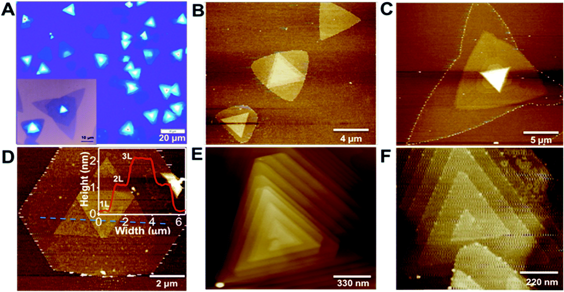 | ||
| Fig. 1 Morphological characterization of pyramid-like and spiral structures of few-layered WS2. (A) Optical image of pyramid-like WS2 domains with ∼20 μm size. Merged triangular domains along with few monolayer WS2 are also seen. Inset shows the optical image of stacked morphology of merged monolayer triangular domains. Inverted triangular domains are seen at the center of the pyramid. (B–D) AFM images of different stacked morphologies of few-layered WS2, with inverted stacking of triangular domains. Inset of (D) shows AFM height profile clearly showing multiple steps indicating stacked layers. (E) AFM image of pyramid-like few-layer LBL grown WS2 and (F) AFM image of few-layer spiral WS2 domain. | ||
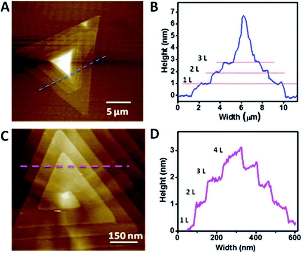 | ||
| Fig. 2 AFM analysis of WS2 structures with LBL and spiral stacking morphologies. (A) AFM image and (B) AFM height profile of a LBL stacked pyramidal WS2. Multiple layers stack one over other forming a pyramid with a step height of ∼1 nm and a terrace width of ∼64 nm. The pyramid-like WS2 has about 7–8 layers. (C) AFM image of a spiral few-layer WS2 structure and the corresponding (D) height profile along the marked line. AFM height profile clearly show step heights of ∼1 nm and a terrace width of ∼50 nm. | ||
A detailed analysis of the growth mechanism will be discussed in the following section. The precursor concentration in CVD growth is very critical, for example, a spike in the sulphur supersaturation in the initial growth stage has been shown to result in a defect driven growth in MoS2.22 In WS2 CVD growth, it is important to carry out the growth in a sulphur rich environment, as the early introduction of sulphur would result in a situation where-in there will not be any WO3 precursor melt ready for the growth, but if delayed, may lead to bulk WS2 growth.26 Different morphologies of WS2 flakes were synthesized under optimized growth conditions. A statistical analysis based on the AFM images of WS2 flakes grown with 0.2 mg ml−1 concentration of WO3 show more than 50–55% domains with stacked morphology which includes 2% of hexagon–hexagon, 4% of hexagon-triangle and 49% of triangle–triangle stacking, while the rest of the flakes are single layered. The ratio seems to vary from point to point on the substrate, due to the use of solid precursors.
Scanning electron microscopy (SEM) and transmission electron microscopy (TEM) were employed to study the microscopic and structural features of pyramid-like WS2 flakes. Fig. 3A and B respectively show the SEM images of ∼10 μm size LBL and spirally stacked thick pyramid-like WS2 flakes. For TEM measurements, WS2 flakes were transferred onto TEM grids by etching the SiO2 layer (detailed procedure given in Methods). TEM image of a typical spirally stacked WS2 flake is shown in Fig. 3C. The characteristic features of pyramid shaped WS2 flakes including the plateau region, stacked and spiral features are clearly observed in SEM and TEM images, and are in accordance with the AFM images. A flat and clean surface was observed on top of the LBL stacked WS2 flake (Fig. 3A), while a random shaped narrow region was observed on top of the spiral WS2 flake (Fig. 3B). Inset of Fig. 3C shows the selected area electron diffraction (SAED) pattern taken from the marked spot in the spiral WS2 in Fig. 3C, which clearly shows a set of hexagonally arranged diffraction spots indicative of highly crystalline nature of the flake. Further, X-ray photoelectron spectroscopy (XPS) was used to confirm the elemental composition of the WS2 flakes (ESI Fig. S3†). Peaks observed at 35.6 eV, and 33.4 eV corresponding to W4f5/2, and W4f7/2 respectively, indicate the presence of W4+ oxidation state.27 The observed peak at 38.7 eV correspond to the presence of W6+ species within the material, most likely from WO3. Peaks positioned at 162.3 eV and 163.57 eV are attributed to S2p3/2 and S2p1/2 of divalent sulphide ions.28
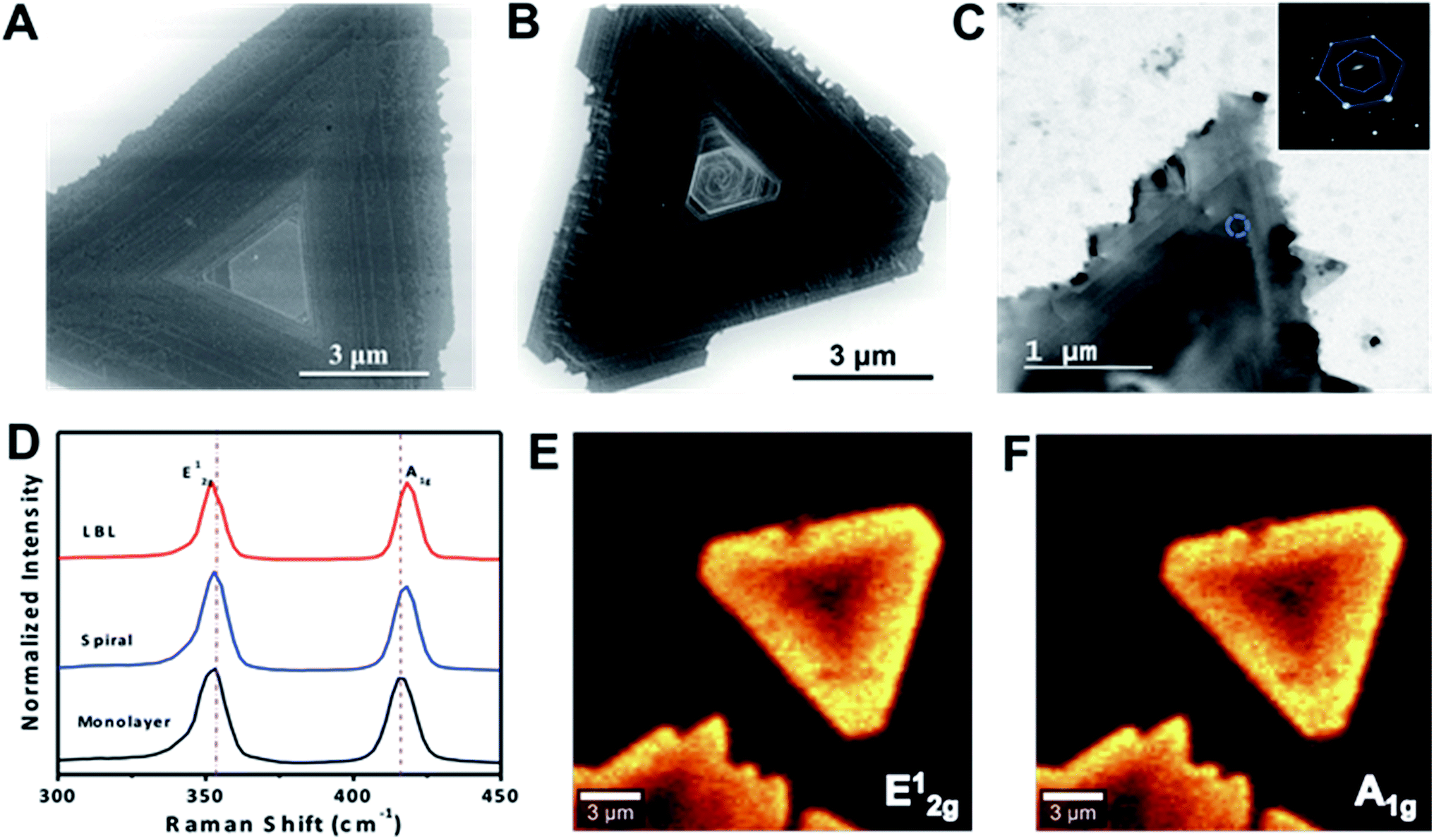 | ||
| Fig. 3 Structural and Raman characterization of pyramid-like and spiral structures of multi-layered WS2. SEM image of multi-layer (A) LBL stacked and (B) spiral WS2 structures. (C) TEM image of a spiral WS2 domain. SAED pattern taken from the marked point is shown as inset in (C). (D) Raman spectra collected from LBL, spiral and monolayer WS2 domains obtained using 488 nm excitation, showing peaks corresponding to E2g1 and A1g modes of vibration. A slight shift in the peak position is observed. (E) and (F) Raman intensity mapping of E2g1 and A1g peaks using 488 nm excitation. Both the images show bright edges compared to dark center, indicative of stacked layers at the center of the pyramid-like WS2. | ||
To investigate the optical properties of spiral and LBL stacked WS2, Raman spectroscopy measurements were recorded (Fig. 3D). The Raman spectra collected in the range 300–500 cm−1 for single layer, spiral and LBL stacked WS2 show two characteristic peaks around 350 and 419 cm−1 corresponding to the in-plane E2g1 and out-of-plane A1g modes of vibration, respectively. A slight shift in the peak position is observed for the stacked WS2 flakes compared to monolayer WS2, indicative of the layer thickness of the flake. Raman mapping was also done for the spiral WS2 flake by using 488 nm excitation. The Raman intensity mapping images for E2g1 and A1g modes of vibration clearly show variation of Raman peak intensity with number of layers (Fig. 3E and F), with darker areas at the center compared to other region, indicative of stacked layers at the center of the pyramid-like WS2. However, uniform Raman peak intensity was observed for E2g1 + 2LA(M) and A1g modes of vibration for monolayer WS2 film, clearly showing uniformly bright triangular domain (ESI Fig. S4†).
To further explore the optical properties of pyramidal WS2 structures, we studied the photoluminescence (PL) properties of spiral WS2 flakes (Fig. 4). Fig. 4A shows the PL spectra from a single WS2 pyramidal flake recorded from its edge, which is typically a monolayer (marked as 1) and from the center, which could be a spiral or multi-layered stack (marked as 2). The strong PL peak centered at ∼630 nm corresponds to the A-exciton resonance2 and the observed peak energy (∼1.97 eV) is consistent with the earlier reported values for monolayer WS2.5,29,30 The edge of the triangular pyramidal WS2 flake is a monolayer as evident from the AFM image (Fig. 2A), and hence exhibit very strong PL emission, being a direct bandgap material. The PL from the centre portion of the pyramid, which corresponds to a few-layer stacked WS2, is much reduced and slightly red-shifted (∼650 nm) due to interlayer coupling. Further, PL emission from the center of the multi-layered spiral and LBL stacked WS2 flakes has been obtained in an extended wavelength region (Fig. 4B). Multi-layered LBL stacked WS2 has an indirect bandgap which gives rise to a new PL peak at ∼900 nm. On the other hand, spiral WS2 structure showed a PL peak at ∼630 nm with almost similar intensity as LBL stacked WS2. However, peak corresponding to lower energy indirect exciton transition was absent here. This could be due to the presence of metallic edges in the spiral WS2 structures at which the non-radiative recombination of excitons dominates.22,31
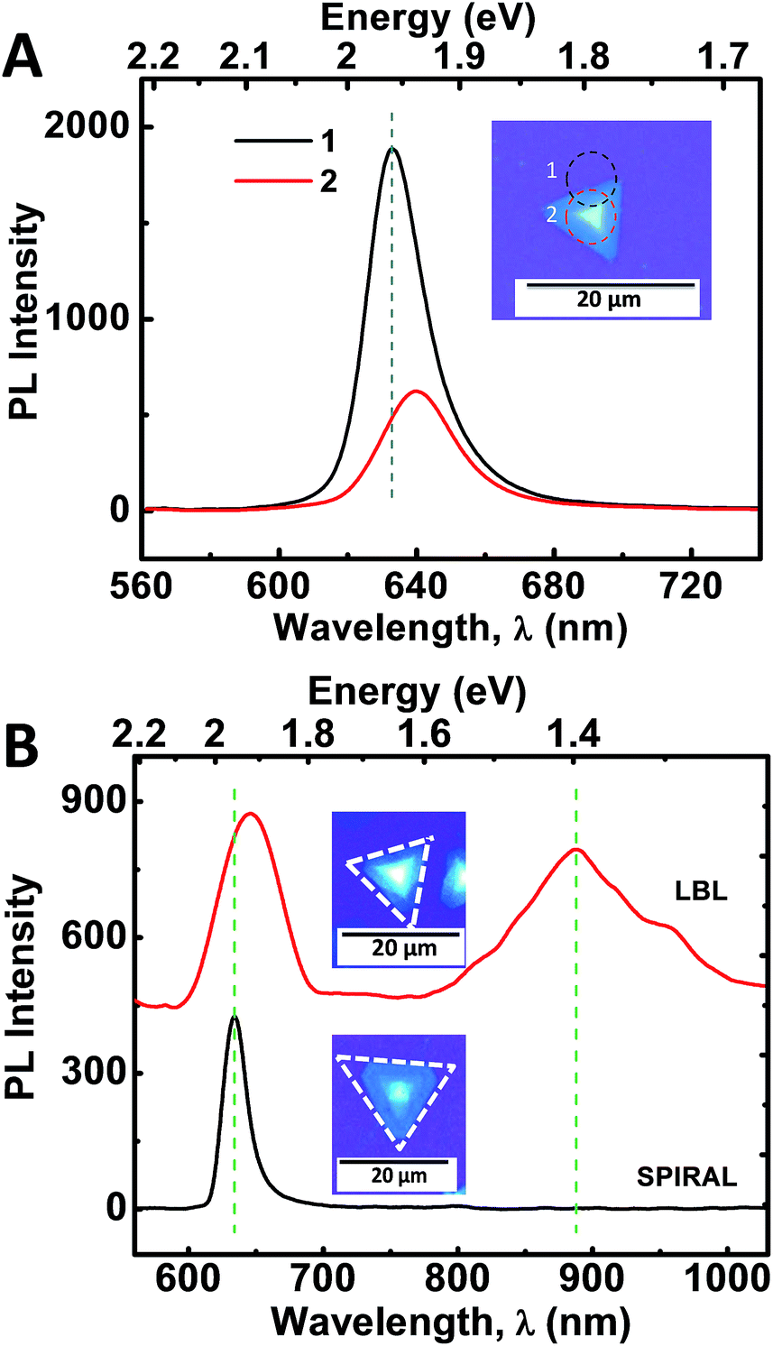 | ||
| Fig. 4 Photoluminescence measurements of stacked WS2 structures. (A) PL spectra collected from two different regions of a single pyramidal WS2 flake, from the edge (1) and center (2) in the wavelength range of 560–740 nm. Inset shows the optical image of the pyramidal WS2 flake with marked regions from where the PL spectrum has been collected. (B) PL spectra obtained in the wavelength range of 550–1050 nm for multi-layered LBL stacked and spiral WS2 flakes. | ||
It is interesting to observe several spiral structures of WS2, both triangular and hexagonal, grown from multiple nucleation sites on a larger hexagonal spiral WS2 flake (Fig. 5A). The spirals are observed to be either left- or right-handed, as shown in Fig. 5B. Similar observation has been reported for spiral MoS2 flakes grown via CVD technique.22 Another interesting observation is the appearance of very thin ribbon-like features on top of the LBL stacked WS2 pyramid (ESI Fig. S5†). Fig. 5C shows another interesting morphology of stacked WS2 domains where in the domains show alternate stacking having the same plateau region on top. Schematic of such morphology is given as inset of Fig. 5C. Thus the overall growth mechanism for the pyramid-shaped WS2 flakes appears to be rather complex and is not well understood. However, several of such pyramidal growths observed in 1D and 2D nanomaterials are explained based on the basic understanding of classical crystal growth theory, wherein the supersaturation of the system drives different growth modes such as screw-dislocation-driven (SDD) growth, layer-by-layer (LBL) growth and dendritic growth.32 Here, we believe that the spirally stacked WS2 pyramidal structures follow SDD growth model, which is the most favourable mode of growth at low supersaturation. Screw dislocations developed under low supersaturation conditions create step edges (slipped planes) in the bottom layer, as shown in Fig. 5D that act as nucleation sites for further addition of precursor atoms leading to the growth of second layer on top of the bottom layer. This gradually leads to the continuous growth of spirals, resulting in a pyramidal growth. Dislocation-driven growth model has been used to explain different morphologies observed in variety of nanostructures including nanowires, nanotubes, 2D nanoplates, branched 3D nanostructures etc.33–35 To obtain pyramidal growth, as in the present work, the dislocation created in the bottom layer grows both in the vertical direction as well as lateral direction (triangular monolayer growth). The difference in the velocity of vertical step growth and the lateral monolayer growth determines the slope of the pyramid formed.36 For the CVD growth, tungsten precursor was introduced as WO3 particles coated onto Si/SiO2 substrate, which forms island-like film upon annealing at the growth temperature (900 °C) in the absence of sulphur, as shown in ESI Fig. S6.† The wide variety of morphologies observed here (Fig. 1) could be due to the variation of precursor concentration over the substrate from point to point (due to the use of solid precursors). The concentration of the reactants typically determines the growth mode, and with high concentration, we expect mostly LBL or multilayer growth.
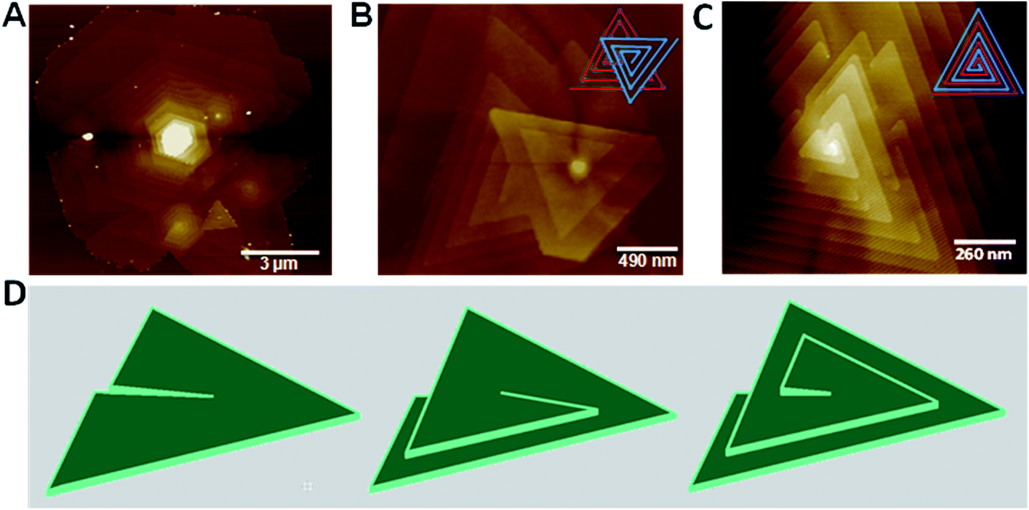 | ||
| Fig. 5 Growth mechanism of spiral WS2. (A) AFM image of a large WS2 domain with multi-centered dislocation driven growth. (B) AFM image of a multi-centered stacked WS2 showing both left- and right-handed spirals. Inset shows the schematic of the multi-centered growth. (C) AFM image of WS2 domains with alternately stacked spirals having the same plateau region. Inset shows the growth model. (D) Schematic illustration of screw dislocation driven growth. Initially, the basal plane is uplifted. Towards the exposed edges, atoms will start to diffuse and the layer starts to grow over the base layer and further continue to grow ending up in pyramid-like spiral structure. | ||
The growth mechanism is more complicated in actual crystals. Initially, crystals grow by LBL mechanism up to a critical size. If this critical size is exceeded, a transition from LBL to multilayer mechanism takes place, and the growth front consists of several monolayers which grow simultaneously.36 With 0.2 mg ml−1 concentration of WO3 particles, growth of spiral WS2 flakes were predominantly observed. However, when tungsten precursor amount is increased by drop casting concentrated dispersion of WO3 powder (0.5 mg ml−1 in ethanol), keeping all other growth parameters same including the substrate area, more than 10–15% growth is observed to be with LBL stacked morphology and remaining are SDD/few-layer domains (ESI Fig. S7†). Here, several merged triangular domains and clustered growth of WS2 are observed, which could be due to the higher growth rate and supersaturation. With a much lesser tungsten precursor (0.1 mg ml−1 in ethanol) and with all other growth parameters kept unchanged, we obtained mostly monolayer triangular WS2 domains (ESI Fig. S4†). Further, CVD growth has been performed by varying the growth temperature from 700 °C to 950 °C keeping all other parameters in the CVD process, including argon gas flow rate (200 sccm), sulphur amount (500 mg) and WO3 concentration (0.2 mg ml−1 in ethanol), unchanged (ESI Fig. S8†). 900 °C appears to be the optimum growth temperature for few-layer pyramid-like WS2 domains, under the given conditions.
Conclusions
To conclude, we have demonstrated a controllable CVD process for the synthesis of spiral and few-layered WS2 nanostructures by varying the precursor concentration. Interesting morphologies of WS2 flakes with spiral and layer-by-layer stacked domains were observed. The growth mechanism for the pyramid-like structures formed by spiral stacking of WS2 monolayers, was discussed based on screw-dislocation-driven (SDD) growth model. The layer dependent optical properties of few-layered and multi-layered WS2 spirals and pyramids were studied by photoluminescence measurements. These few-layered spiral WS2 structures with interesting optical properties could be used for optoelectronics device applications.Methods
Substrate cleaning
Si/SiO2 substrates are first sonicated in distilled water, isopropanol and acetone for 10 min each and then dried in nitrogen flow. The dried sample was immersed in piranha solution for 10 min and again sonicated in water, isopropanol and acetone. This was followed by plasma cleaning for 20 min using Harrick Plasma Cleaner PDC-32G.WS2 growth
Monolayer, as well as pyramidal WS2 domains were grown on Si/SiO2 (290 nm SiO2) by direct sulphurization of WO3 precursor. First, WO3 powder (Aldrich puriss 99.9%) is dispersed in ethanol and 10 μl of dispersion was drop-casted onto Si/SiO2 after sonicating for 30 min. Tungsten precursors with different concentrations (0.1 mg ml−1, 0.2 mg ml−1 and 0.5 mg ml−1) were used. The substrates were placed inside a quartz tube reactor (tube length 120 cm; 5 cm diameter), kept in a single zone tubular furnace (Thermo scientific Lindberg Blue M) along with 500 mg of sulphur powder (Aldrich, purum 99.5%). Sulphur powder was placed upstream towards the cooler side of the reactor. Quartz tube was evacuated for 30 min and refilled 3–4 times with UHP argon to completely remove oxygen from the reaction zone. A steady flow of argon at 200 sccm was maintained throughout the experiment. The furnace was heated to the reaction temperature as shown in ESI Fig. S1.† By this time, the temperature in the vicinity of sulphur powder reaches its evaporation temperature and the sulphur fumes are carried towards the reaction zone by argon gas. After the deposition, furnace is allowed to cool naturally.TEM sample preparation
PMMA (950A4 resist) was spin coated on the WS2 grown Si/SiO2 substrates at 2000 rpm for 1 min, followed by baking at 180 °C for 20 min. A free standing PMMA polymer layer on top of the solution is obtained by etching the SiO2 layer by using 3 M NaOH solution. The PMMA layer is scooped and dipped in distilled water for a day to remove NaOH content and later was scooped and transferred directly onto TEM grid and allowed to dry. After drying in room temperature, PMMA was removed by using hot acetone bath and the grid was kept for drying in vacuum and later used for imaging.Characterization
The samples were characterized by using optical microscope (Olympus BX41), Atomic Force Microscope (Bruker Edge), Raman spectrometer (Horiba Jobin YVON), scanning electron microscope (Nano SEM 450), transmission electron microscope (Tecnai F20/30, 200 keV) and X-ray photoelectron spectrometer (Kratos Analytical Axis Ultra). For PL measurements we used a 532 nm laser (photon energy 2.33 eV). The laser beam was focused to a spot of diameter ∼6 μm. The PL was collected using a 10× objective and was recorded using a monochromator (Horiba Scientific iHR320) and a CCD.Acknowledgements
PVS acknowledges UGC, Govt. of India for the financial support and PKB acknowledges support from DST, India through Inspire Fellowship. RNK acknowledges partial support for this work from SERB, India under Fast Track Scheme for Young Scientists. The work has been supported by a start-up grant to MMS from Indian Institute of Science Education and Research (IISER) Thiruvananthapuram, Kerala, INDIA.Notes and references
- D. Braga, I. Gutiérrez Lezama, H. Berger and A. F. Morpurgo, Nano Lett., 2012, 12, 5218–5223 CrossRef CAS PubMed.
- H. R. Gutiérrez, N. Perea-López, A. L. Elías, A. Berkdemir, B. Wang, R. Lv, F. López-Urías, V. H. Crespi, H. Terrones and M. Terrones, Nano Lett., 2013, 13, 3447–3454 CrossRef PubMed.
- B. Radisavljevic, A. Radenovic, J. Brivio, V. Giacometti and A. Kis, Nat. Nanotechnol., 2011, 6, 147–150 CrossRef CAS PubMed.
- D. J. Late, Y.-K. Huang, B. Liu, J. Acharya, S. N. Shirodkar, J. Luo, A. Yan, D. Charles, U. V. Waghmare, V. P. Dravid and C. N. R. Rao, ACS Nano, 2013, 7, 4879–4891 CrossRef CAS PubMed.
- N. Huo, Z. Wei, X. Meng, J. Kang, F. Wu, S.-S. Li, S.-H. Wei and J. Li, J. Mater. Chem. C, 2015, 3, 5467–5473 RSC.
- S. Wi, H. Kim, M. Chen, H. Nam, L. J. Guo, E. Meyhofer and X. Liang, ACS Nano, 2014, 8, 5270–5281 CrossRef CAS PubMed.
- T. Stephenson, Z. Li, B. Olsen and D. Mitlin, Energy Environ. Sci., 2014, 7, 209–231 CAS.
- M. A. Lukowski, A. S. Daniel, C. R. English, F. Meng, A. Forticaux, R. J. Hamers and S. Jin, Energy Environ. Sci., 2014, 7, 2608–2613 CAS.
- Y. Yan, B. Xia, N. Li, Z. Xu, A. Fisher and X. Wang, J. Mater. Chem. A, 2015, 3, 131–135 CAS.
- J. Lin, Z. Peng, G. Wang, D. Zakhidov, E. Larios, M. J. Yacaman and J. M. Tour, Adv. Energy Mater., 2014, 4, 1301875 Search PubMed.
- J. D. Benck, T. R. Hellstern, J. Kibsgaard, P. Chakthranont and T. F. Jaramillo, ACS Catal., 2014, 4, 3957–3971 CrossRef CAS.
- Y. Yan, B. Xia, X. Ge, Z. Liu, J.-Y. Wang and X. Wang, ACS Appl. Mater. Interfaces, 2013, 5, 12794–12798 CAS.
- D. Gopalakrishnan, D. Damien and M. M. Shaijumon, ACS Nano, 2014, 8, 5297–5303 CrossRef CAS PubMed.
- D. Gopalakrishnan, D. Damien, B. Li, H. Gullappalli, V. K. Pillai, P. M. Ajayan and M. M. Shaijumon, Chem. Commun., 2015, 51, 6293–6296 RSC.
- J. Park, W. Lee, T. Choi, S.-H. Hwang, J. M. Myoung, J.-H. Jung, S.-H. Kim and H. Kim, Nanoscale, 2015, 7, 1308–1313 RSC.
- C. Cong, J. Shang, X. Wu, B. Cao, N. Peimyoo, C. Qiu, L. Sun and T. Yu, Adv. Opt. Mater., 2014, 2, 131–136 CrossRef.
- Y. Zhang, Y. Zhang, Q. Ji, J. Ju, H. Yuan, J. Shi, T. Gao, D. Ma, M. Liu, Y. Chen, X. Song, H. Y. Hwang, Y. Cui and Z. Liu, ACS Nano, 2013, 7, 8963–8971 CrossRef CAS PubMed.
- J.-K. Huang, J. Pu, C.-L. Hsu, M.-H. Chiu, Z.-Y. Juang, Y.-H. Chang, W.-H. Chang, Y. Iwasa, T. Takenobu and L.-J. Li, ACS Nano, 2014, 8, 923–930 CrossRef CAS PubMed.
- X. Wang, Y. Gong, G. Shi, W. L. Chow, K. Keyshar, G. Ye, R. Vajtai, J. Lou, Z. Liu, E. Ringe, B. K. Tay and P. M. Ajayan, ACS Nano, 2014, 8, 5125–5131 CrossRef CAS PubMed.
- J. Xia, X. Huang, L.-Z. Liu, M. Wang, L. Wang, B. Huang, D.-D. Zhu, J.-J. Li, C.-Z. Gu and X.-M. Meng, Nanoscale, 2014, 6, 8949–8955 RSC.
- Y. Rong, Y. Fan, A. Leen Koh, A. W. Robertson, K. He, S. Wang, H. Tan, R. Sinclair and J. H. Warner, Nanoscale, 2014, 6, 12096–12103 RSC.
- L. Zhang, K. Liu, A. B. Wong, J. Kim, X. Hong, C. Liu, T. Cao, S. G. Louie, F. Wang and P. Yang, Nano Lett., 2014, 14, 6418–6423 CrossRef CAS PubMed.
- L. Chen, B. Liu, A. N. Abbas, Y. Ma, X. Fang, Y. Liu and C. Zhou, ACS Nano, 2014, 8, 11543–11551 CrossRef CAS PubMed.
- S. Jin, M. J. Bierman and S. A. Morin, J. Phys. Chem. Lett., 2010, 1, 1472–1480 CrossRef CAS.
- J. W. Ostrander, A. A. Mamedov and N. A. Kotov, J. Am. Chem. Soc., 2001, 123, 1101–1110 CrossRef CAS PubMed.
- W. Zhao, Z. Ghorannevis, K. K. Amara, J. R. Pang, M. Toh, X. Zhang, C. Kloc, P. H. Tan and G. Eda, Nanoscale, 2013, 5, 9677–9683 RSC.
- X. Mao, Y. Xu, Q. Xue, W. Wang and D. Gao, Nanoscale Res. Lett., 2013, 8, 430 CrossRef PubMed.
- A. Ambrosi, Z. Sofer and M. Pumera, Chem. Commun., 2015, 51, 8450–8453 RSC.
- Q. Fu, W. Wang, L. Yang, J. Huang, J. Zhang and B. Xiang, RSC Adv., 2015, 5, 15795–15799 RSC.
- X. H. Wang, J. Q. Ning, C. C. Zheng, B. R. Zhu, L. Xie, H. S. Wu and S. J. Xu, J. Mater. Chem. A, 2015, 3, 2589–2592 CAS.
- M. V. Bollinger, J. V. Lauritsen, K. W. Jacobsen, J. K. Nørskov, S. Helveg and F. Besenbacher, Phys. Rev. Lett., 2001, 87, 196803 CrossRef CAS PubMed.
- S. A. Morin, A. Forticaux, M. J. Bierman and S. Jin, Nano Lett., 2011, 11, 4449–4455 CrossRef CAS PubMed.
- M. J. Bierman, Y. K. A. Lau, A. V. Kvit, A. L. Schmitt and S. Jin, Science, 2008, 320, 1060–1063 CrossRef CAS PubMed.
- H. Wu, F. Meng, L. Li, S. Jin and G. Zheng, ACS Nano, 2012, 6, 4461–4468 CrossRef CAS PubMed.
- F. Meng, S. A. Morin, A. Forticaux and S. Jin, Acc. Chem. Res., 2013, 46, 1616–1626 CrossRef CAS PubMed.
- I. V. Markov, Crystal Growth for Beginners: Fundamentals of Nucleation, Crystal Growth and Epitaxy, World Scientific, New Jersey, 2nd edn, 2004 Search PubMed.
Footnote |
| † Electronic supplementary information (ESI) available. See DOI: 10.1039/c5ra23020a |
| This journal is © The Royal Society of Chemistry 2016 |