DOI:
10.1039/C5NR07036H
(Paper)
Nanoscale, 2016,
8, 2727-2739
Facile synthesis of SnO2–PbS nanocomposites with controlled structure for applications in photocatalysis†
Received
11th October 2015
, Accepted 12th December 2015
First published on 14th December 2015
Abstract
Recent studies have shown that SnO2-based nanocomposites offer excellent electrical, optical, and electrochemical properties. In this article, we present the facile and cost-effective fabrication, characterization and testing of a new SnO2–PbS nanocomposite photocatalyst designed to overcome low photocatalytic efficiency brought about by electron–hole recombination and narrow photoresponse range. The structure is fully elucidated by X-ray diffraction (XRD)/Reitveld refinement, Raman spectroscopy, X-ray photoelectron spectroscopy (XPS), Brunauer–Emmett–Teller (BET) surface area analysis, and transmission electron microscopy (TEM). Energy-dispersive X-ray spectroscopy (EDX) spectrum imaging analysis demonstrates the intermixing of SnO2 and PbS to form nanocomposites. A charge separation mechanism is presented that explains how the two semiconductors in junction function synergistically. The efficacy of this new nanocomposite material in the photocatalytic degradation of the toxic dye Rhodamine B under simulated solar irradiation is demonstrated. An apparent quantum yield of 0.217 mol min−1 W−1 is calculated with data revealing good catalyst recyclability and that charge separation in SnO2–PbS leads to significantly enhanced photocatalytic activity in comparison to either SnO2 or PbS.
Introduction
The term ‘nanocomposite’ is used to describe a multiphase solid material in which one of the phases has one, two or three dimensions of less than 100 nm.1 Nanocomposites frequently exhibit properties (or a combination of properties) not available through any of the components in the composite individually. The fabrication of nanocomposite materials therefore promises access to previously unachievable properties of technological importance in applications2 including LEDs, lasers, non-linear optical devices3 and bio-labelling.4 In the specific contexts of electrochemistry/photochemistry/photophysics and photoelectrochemistry/photocatalysis, nanocomposite materials have been extensively utilized.5 The unique properties of the nanocomposite materials are generally considered to arise from the interfacial interactions of their component phases,6 with two boundary cases recognized in nanocomposites. The first involves covalent interactions, which seldom form spontaneously, but can be created by particular surface treatments.7 The second involves van der Waals interactions.6 In practice the strength of interfacial interactions are somewhere between these two boundary extremes.8 The unique, size-dependent physical and chemical properties of nanocomposite materials, combined with their high processability and defined chemical and morphological structures, which frequently present unique and tunable characteristics, cannot be achieved by traditional core–shell or heterodimer structure nanomaterials.9
A field that has received significant attention over the last two decades is that of nanocomposites comprising two semiconductors with different band gaps. Such semiconductor-based nanocomposites exhibit properties derived from the interfacial interactions of their component phases. Additionally, size-quantized optical and optoelectronic effects bring an innovative dimension to research as both the photonic characteristics of semiconductor particles are significantly modified in the (sub-)nanometer regime.10,11 One consequence of this is that nanocomposites of semiconductor materials are attracting considerable attention in the context of developing devices such as light emitting diodes and solar cells,12–14 solar photovoltaic devices and chemical/biological sensors.15
A significant number of semiconductor-based nanocomposites have been reported.5 Central to the present study are systems based on SnO2. These have the advantages that SnO2 is a stable oxide semiconductor with a wide n-type band gap of 3.6 eV (ref. 16) and that it is both low cost and non-toxic. SnO2 has been applied in the fields of solar cells,17 catalytic support materials,18 transparent electrodes,19 and solid-state chemical sensors.20 Recent years have seen efforts to control the synthesis of SnO2-semiconductor nanocomposites in which the valence band and conduction band positions have been modulated in an attempt to increase the carrier lifetime of photolytically induced electrons and holes. For example, Zhang et al.21 prepared SnO2–Ag3PO4 semiconductor nanocomposites which exhibit much higher photocatalytic activity and improved stability relative to pure Ag3PO4 or SnO2, while McCue et al.22 synthesized SnO2–In2O3 nanocomposites that exhibited outstanding sensitivity for both reducing and oxidizing gases. Pan et al.23 have suggested that SnO2–CdS nanocomposites exhibit promise for highly sensitive visible-light photodetectors and efficient photocatalysis. A nanocomposite of iron(III) oxide and tin(IV) oxide, 50![[thin space (1/6-em)]](https://www.rsc.org/images/entities/char_2009.gif) :50 SnO2–Fe2O3 was prepared by Taei et al.24 and revealed excellent electrocatalytic activity towards the oxidation of epinephrine, acetaminophen and tryptophan. SnO2 has also demonstrated the ability to mix with carbon nanotubes,25 carbon,26 and with reduced graphene oxide27 to form SnO2-based nanocomposites.
:50 SnO2–Fe2O3 was prepared by Taei et al.24 and revealed excellent electrocatalytic activity towards the oxidation of epinephrine, acetaminophen and tryptophan. SnO2 has also demonstrated the ability to mix with carbon nanotubes,25 carbon,26 and with reduced graphene oxide27 to form SnO2-based nanocomposites.
SnO2-based nanocomposites containing PbS as the other active component are, to the best of our knowledge, unreported. Such a combination would be extremely desirable, there being a large band gap difference (approximately 3.2 eV) between the two component materials. This offers increased charge separation and promises enhanced electrical, optical, electrochemical, photocatalytic and gas sensing properties. PbS itself is a metal sulfide semiconductor with a narrow bulk bandgap of 0.41 eV at room temperature28 that has applications in fiber optics, telecommunications, lasers, solar cells and biological systems.29 It is established that the optical, electronic and magnetic properties of PbS nanocrystals significantly differ from those of bulk PbS, the band gaps of PbS nanocrystals being significantly blue shifted from the near-IR into the visible and near-UV regions with decreasing particle size.30 It is reasonable, therefore, that these properties can be further modified and exploited by mixing PbS nanocrystals with those of other semiconductors.31
This article presents a facile solution approach by which to synthesize SnO2–PbS nanocomposites, using cetyl trimethyl ammonium bromide (CTAB) as a surface capping agent32 and Pb(NO3)2 and Na2S·9H2O as Pb2+ and S2− sources, respectively (Fig. 1). The aim is to develop a synthetic route which utilizes (i) low temperatures, (ii) shorter reaction times, (iii) safe and inexpensive reagents and (iv) open vessels. This approach is in contrast to recent work aimed at producing nanomaterials for the photochemical passivation of dyes. Such work has, for example, yielded hybrid nanospheres33 by extended and high temperature autoclave methods and by using expensive precious metal colloid. In other work, the synthesis of core@shell heterostructures e.g. of SnO2@CdS has employed precious metal substrates and high temperatures whilst also necessitating the use of highly toxic precursors.23 The structure, morphology and photocatalytic properties of new SnO2–PbS nanocomposites are investigated and a model is developed based upon lattice relaxation processes manifest at the interfacial regions in the nanocomposites, which helps to explain how and why the two semiconductors interact.
 |
| | Fig. 1 Synthetic scheme for the preparation of SnO2–PbS nanocomposites. | |
Experimental section
Synthesis
General synthetic and analytical details.
Chemicals were purchased from Sigma-Aldrich (reagents: analytical grade; solvents: HPLC grade) and used without further purification. Aqueous solutions were prepared using HPLC water (Millipore).
SnO2 nanoparticle preparation.
SnCl4·5H2O (0.351 g, 1.0 mmol) was dissolved in water (25 ml). CTAB (0.365 g, 1.0 mmol) was dissolved in water (5 ml) and added to the SnCl4·5H2O solution. The resulting mixture was stirred vigorously for 1 h until a clear solution was obtained. NaOH (0.8 g, 20.0 mmol) was dissolved in water (10 ml), and to this solution 10 ml of ethanol was added to make a basic mixture of alcohol and water (1:1). This was added dropwise to SnCl4·5H2O solution under continuous stirring. A white precipitate that had formed in the acidic reaction mixture dissolved once a pH of 11–12 was obtained. The solution was heated to reflux at 100 °C for 4 h. After cooling to room temperature, a white colloidal suspension of SnO2 nanoparticles (NPs) was obtained, which was centrifuged and the solid washed with water (×2) and absolute ethanol (×3) to remove impurities before being dried at 60 °C in air.
SnO2–PbS nanocomposite preparation.
To make SnO2–PbS nanocomposites, a soft chemical process (near ambient temperature reaction in an open vessel)34 was used. In a typical process, SnO2 NPs35 (0.015 g, 0.1 mmol) were dispersed in water (25 ml) by ultrasonication. CTAB (0.036 g, 0.1 mmol) was added with vigorous stirring. The resulting dispersion was slowly elevated to 50 °C, retained at this temperature for 2 h and then allowed to cool to room temperature, after which flocculation was seen to have occurred. A 5 ml aqueous solution of Na2S·9H2O (0.024 g, 0.1 mmol) was added dropwise and the resulting mixture stirred for 30 min. Finally, a 5 ml aqueous solution of Pb(NO3)2 (0.033 g, 0.1 mmol) was added dropwise to the system and the mixture stirred vigorously for another 2 h at room temperature. The SnO2–PbS nanocomposite was obtained by centrifugation and washed with water (2 × 25 ml) and absolute ethanol (3 × 25 ml) and then vacuum dried for 6 h to obtain the final product as a grey powder. See Fig. 1 above and for the synthesis of PbS nanocubes (NCs) undertaken using Na2S·9H2O with Pb(NO3)2 in the absence of preformed SnO2 NPs see ESI.†
Nanomaterials characterization
X-ray diffraction (XRD).
XRD profiles were recorded using Ni-filtered Cu Kα radiation from a highly stabilized and automated PAN-analytical X-ray generator operated at 40 kV and 40 mA. The X-ray generator was coupled with a PW3071/60 Bracket goniometer for sample mounting. Step-scan data (step size 0.02° 2θ, counting time 2 s per step) were recorded for 20°–75° 2θ. Powder patterns were deconvoluted using the Rietveld whole-profile fitting method based on structure and microstructure refinement.36 Rietveld software MAUD version 2.3337 was used to carry out simultaneous refinement of both material structure and microstructure by a least squares refinement method. For the detailed procedure see ESI.†
Transmission electron microscopy (TEM).
A Technai 20 high resolution (HR) TEM was used to scrutinize nanocrystal shape and size. Magnification 2.0.1 was used to count the diameters of 100 particles (N), defining intervals of 0.25 nm between dmin ≤ d ≤ dmax. Size distributions were constructed with DataGraph 3.0 and morphology was analyzed using Digital Micrograph 3.6.5. Compositional analysis used a scanning transmission electron microscope (STEM, Technai Osiris). High-angle annular dark field (HAADF) imaging and energy-dispersive X-ray (EDX) spectrum imaging techniques were utilized to characterize individual structures. EDX spectrum image (SI) data was processed using machine learning methods implemented in HyperSpy.38 In each case, analysis required sample preparation by droplet coating of ethanolic suspensions on carbon coated Au grids (Agar Scientific, 300 mesh).
Raman spectroscopy.
Data were collected at room temperature on a Thermo Scientific DXR Raman microscope using a helium–neon laser with an excitation wavelength of 532 nm (laser power 10 mW).
X-ray photoelectron spectroscopy (XPS).
XPS measurements were obtained using a Thermo Scientific K-Alpha system. The binding energy was calibrated internally based on the C 1s line position.
Brunauer–Emmett–Teller (BET) surface area analysis.
BET surface areas of as-prepared samples were analyzed by nitrogen adsorption in a Tristar 3000 analyzer. Samples were degassed at 77 K before nitrogen adsorption measurements were commenced. The BET surface areas were determined by a multipoint BET method using the adsorption data in the P/P0 range 0.0–1.0 (where P and P0 are the equilibrium and the saturation pressure of adsorbates at the temperature of adsorption).
Photocatalytic experiments.
Photocatalytic activities of the as-prepared samples were evaluated by monitoring the degradation of RhB dye in water under simulated solar irradiation without sacrificial reagents at room temperature. In a typical process, 5.0 mg of catalyst was added to 40 ml of a 1.0 × 10⁻⁵ M aqueous solution of RhB (pH 7), and the mixture stirred in the dark for 2 h. to allow adsorption of the dye on the catalyst surface.39 Thereafter, a 3.0 ml aliquot of the mixture was centrifuged and the absorption of the dye solution therein determined to obtain the dye concentration before photocatalysis (C0). The remaining solution was then irradiated with a 150 W xenon lamp fitted with an air mass 1.5 global (AM 1.5G) filter (Solar Simulator model LSO106, 1 sun illumination, 100 mW cm−2). Degradation of the RhB absorption maximum at 555 nm was monitored using a UV-vis spectrophotometer (Perkin Elmer LAMBDA 265) to obtain the concentration (C) of dye as a function of time in subsequent aliquots. An ice cold water bath was used to prevent evaporation during catalysis and to avoid degradation due to heating. Two reference experiments, (i) without light irradiation in the presence of catalyst, and (ii) with light irradiation in the absence of catalyst were also undertaken and the degradation efficiency was calculated according to| | | Degradation (%) = (1 − C/C0) × 100 | (1) |
Apparent quantum yield (ϕx) was measured according to
| | | ϕx = ±(d[x]/dt)/d[hv]inc/dt | (2) |
where d[
x]/d
t is the rate of change of the concentration of the reactant (or product) and d[
hv]
inc/d
t is the total optical power impinging on the sample.
40
Hydroxyl radicals (OH˙) produced during photocatalysis were estimated by the fluorescence method using terephthalic acid (TA) as a probe molecule. In a typical process, a 5.0 mg portion of catalyst was dispersed in an aqueous solution of 30 ml of TA (5 × 10⁻⁴ M) and NaOH (2 × 10⁻³ M). The resulting suspension was exposed to simulated solar radiation and at regular intervals, 3.0 ml of the suspension was collected and centrifuged and the maximum fluorescence emission intensity measured with an excitation wavelength of 315 nm. This method relies on the fluorescence signal at 425 nm of 2-hydroxyterephthalic acid (TAOH).
Results and discussion
Phase identification by XRD
SnO2 NPs and SnO2–PbS nanocomposites were prepared as described above. Fig. 2a shows the XRD pattern for SnO2 NPs, with all peaks indexed with tetragonal SnO2 phase (ICSD code 154960, space group P42/mnm, a = b = 4.7331 Å, c = 3.1815 Å). The breadth of the reflections indicates that the SnO2 NPs are relatively small.41 (For the XRD pattern of PbS NCs see ESI Fig. S1.†) The XRD pattern of the SnO2–PbS nanocomposites (Fig. 2b) is similar to that of the SnO2 NPs, the intensity ratio of the first two peaks (at low 2θ) notwithstanding. In Fig. 2a the intensity ratio of these (110) and (101) reflections is essentially unity, but in Fig. 2b the (110) reflection appears more intense. This variation in the intensity ratio is attributed to the presence of peak overlap between PbS (111) and SnO2 (110). The same is true for SnO2 (211) and PbS (311). However, other reflections consistent with PbS are almost absent from the XRD pattern of SnO2–PbS nanocomposites, indicating that the PbS component is rendered significantly amorphous by virtue of its including a high degree of lattice imperfections. Resulting changes in microstructual parameters are summarized in Tables 1 and 2.
 |
| | Fig. 2 Observed (IO) and simulated (IC) XRD patterns (indexed) of (a) SnO2 NPs and (b) SnO2–PbS nanocomposites. The green lines represent IO–IC. Vertical markers corresponding to reflections from individual phases are shown in blue. | |
Table 1 Microstructural parameters obtained for SnO2 NPs
| Lattice parameters (Å) |
Anisotropic particle size (nm) |
Direction (plane) |
Anisotropic lattice strain |
|
a
|
c
|
| 4.7764 |
3.2558 |
2.11 |
110 |
0.0058 |
|
|
|
4.59 |
101 |
0.0408 |
|
|
|
2.39 |
200 |
0.0783 |
|
|
|
3.40 |
211 |
0.0248 |
|
|
|
3.12 |
112 |
0.0482 |
|
|
|
4.74 |
301 |
0.0182 |
Table 2 Microstructural parameters obtained for SnO2–PbS nanocomposites
| Phase |
Vol. fraction |
Lattice parameters (Å) |
Particle size (nm) |
Strain |
Fractional coordinate of oxygen |
|
a
|
c
|
x
|
y
|
| SnO2 (P42/mnm) |
79.88 |
4.7845 |
3.2247 |
2.89 |
0.020 |
0.3465 |
0.1845 |
PbS (Fm![[3 with combining macron]](https://www.rsc.org/images/entities/char_0033_0304.gif) m) m) |
20.12 |
5.9746 |
2.60 |
0.041 |
|
|
Nanostructure evolution by X-ray diffraction
To interrogate micro/nano-structural defect parameters information related to, for example, signal full width at half-maximum (FWHM), intensity maxima, integrated intensity, and Gaussian content (Gaussianity)42 was extracted using Rietveld analysis.43 This method considers the isolated and overlapping reflections of all pertinent phases in a multiphase material and, in the present study, has been used to evaluate different structure/microstructure parameters in SnO2 NPs and SnO2–PbS nanocomposites (Fig. 2). The Goodness-of-Fit value of each fitted pattern lies very close to unity. At a = 4.7764 Å and c = 3.2558 Å, the lattice parameters obtained for SnO2 NPs from the Rietveld refinement are slightly larger than the reported values (ICSD code 154960, a = 4.7331 Å, c = 3.1815 Å), suggesting an expansion of the unit cell volume from 71.272 Å3 to 74.277 Å3 as the particle size reduces to nanometer regime. Broadening of reflections results from the cumulative effect of both small particle size and r.m.s lattice strain, both of which are found to be anisotropic (Table 1).
The presence of cubic PbS phase alongside tetragonal SnO2 phase is clearly revealed by Fig. 3a, which highlights the significant intensity mismatches that result if the XRD pattern for SnO2–PbS nanocomposites is fitted with only tetragonal SnO2 phase. Data indicate the presence of a small amount of PbS in the composite with very small particle size. The poor refinement quality in Fig. 3a significantly improves if the same XRD pattern is fitted with both SnO2 and PbS phases (Fig. 3b). Refinement suggests that the composite comprises a major SnO2 phase (∼80 vol%) and a minor PbS phase (∼20 vol%). The individual contribution of each of these phases along with the general background intensity in the XRD pattern is shown in Fig. 3c. Interestingly, and in contrast to either SnO2 or PbS, particle size and r.m.s lattice strain in the nanocomposites are isotropic in nature. In the nanocomposite, PbS is rather amorphous, resulting in the observation of very broad reflections centered around the most intense reflections of bulk PbS which coincide with the nanocrystalline SnO2 reflections. The nature of the PbS component of the nanocomposite explains the lack of strong crystalline reflections attributable to PbS in the XRD pattern. It is also evident in Table 2 that the particle size of this PbS has been significantly reduced relative to that seen for pure PbS. Moreover, the highly distorted cubic phase with the extended a value demonstrates approximately four times as much lattice strain as nanocrystalline PbS (Table S1†).
 |
| | Fig. 3 Typical Rietveld refinement output pattern for SnO2–PbS nanocomposites employing (a) tetragonal SnO2 phase only and (b) both tetragonal SnO2 and cubic PbS phase. (c) The contribution of tetragonal SnO2, cubic PbS and background to the XRD pattern for SnO2–PbS nanocomposites. | |
To understand the changes associated with different microstructural parameters in the atomic arrangements in SnO2 NPs, PbS NCs and SnO2–PbS nanocomposites atomic models of tetragonal SnO2 (Fig. S3), cubic PbS (Fig. S4) and SnO2–PbS nanocomposites (Fig. S5) have been designed and are analyzed critically in the ESI.†
TEM analysis
TEM and HRTEM images and fast Fourier transform (FFT) patterns of SnO2 NPs are given in Fig. 4 and S6.†Fig. 4 demonstrates the presence of NPs of mean size of 4.2 ± 1.0 nm; the measured fringe spacing being 0.33 nm, suggesting the (110) plane of tetragonal SnO2.16 (For representative TEM images and an FFT pattern of PbS NCs see ESI Fig. S7 and S8.†)
 |
| | Fig. 4 A representative HRTEM image of SnO2 NPs indicating measured distances between the lattice planes and the particle size distribution for the sample (top left). The area in the red circle was subjected to FFT (see ESI Fig. S6b†). | |
Preliminary TEM images of SnO2–PbS nanocomposites suggest the formation of a composite structure (see Fig. S9†). To further elucidate this STEM–HAADF imaging and EDX spectrum imaging techniques were employed. The separation of component signals using independent component analysis (ICA) allows for reconstruction of the heterogeneous nanocomposite using a method which, unlike in conventional EDX mapping, is free of external bias, except for the choice of the number of components. ICA, implemented in HyperSpy,38 was carried out on an EDX spectrum image (unprocessed EDX data is shown in ESI Fig. S10 and 11†). The multi-dimensional dataset was reduced and projected onto five maximally independent dimensions labeled IC#0 to IC#4 in Fig. 5 (see also ESI†). IC#0 contains both Cu-Kα and Au-Lα and -Mα peaks, which likely originate from secondary scattering by Cu in the sample holder and Au in the support grid, respectively. IC#1 contains Pb-L, Pb-M, Cu-Kα and S-Kα X-ray lines. Ignoring the Cu-Kα peak, the pairing of Pb and S X-ray lines in the component spectrum is strong evidence that the X-rays originate from a Pb-S compound.44 IC#2 contains Sn-K, Sn-L, Cu-Kα, Si-Kα and N-Kα peaks (the last two we attribute to minor contamination). It is expected that if a SnO2 compound is present then both Sn and O peaks should be a captured in a single component, as was the case for IC#1. However, the very low energy oxygen peak suffers from strong attenuation in the sample on the path to the detector, causing variability in the signal strength of O relative to Sn as a function of location. This may explain why ICA has isolated oxygen as a single component (IC#4). Finally, IC#3 contains only a C-Kα peak, and it is mapped to the location of the amorphous holey carbon support film as expected.
 |
| | Fig. 5 ICA results obtained from an EDX spectrum image of a SnO2–PbS nanocomposite structure. (a) Independent component spectra containing the X-ray lines for the elements present (Au and Cu attributable to grid and sample holder). Independent component maps (b) IC#0-#4 are interspersed throughout the region. IC#1 represents a Pb rich phase, IC#2 a Sn rich phase, and IC#3 the carbon supporting film. Bottom right is an artificially coloured overlay of the IC#1 (green) and IC#2 (red) maps. | |
Raman spectroscopy
Raman spectroscopy was applied to the structural characterization of the SnO2 NPs and SnO2–PbS nanocomposites. The SnO2 NPs are rutile in nature and occupy the space group P42/mnm (D4h), having the Raman active modes B1g, Eg, A1g, and B2g. Fig. 6a shows the spectrum of SnO2 NPs at room temperature, revealing peaks at 484 cm−1, 571 cm−1 and 762 cm−1. Those at 484 cm−1 and 762 cm−1 are consistent with rutile bulk SnO245 and that at 571 cm−1 is attributable to a SnO2 nanocrystal surface defect.46 Broadening of the B2g peak in comparison to that of bulk SnO2 is also characteristic of the nanocrystalline nature of the sample.45 Moreover, the relative contribution of the defect-related peak at 571 cm−1 (mostly due to surface oxygen vacancies)47 is large compared to the main Raman active modes for SnO2 by virtue of the large surface area of the small SnO2 NPs. Fig. 6b shows the Raman spectrum of SnO2–PbS nanocomposites. The strong peak at 630 cm−1 is assigned to SnO2 NPs,26 whereas peaks at 486 cm−1 and 768 cm−1 are consistent with rutile bulk SnO2.45 The existence of PbS in the nanocomposite is indicated by the strong peak at 972 cm−1 (for Raman data on PbS NCs at room temperature see ESI Fig. S12†).48 Moreover, the peak in Fig. 6a attributed to a SnO2 nanocrystal surface defect mode is translated to the spectrum of the nanocomposite at 630 cm−1, indicating that SnO2 nanocrystallite surfaces are modified by the inclusion of PbS.
 |
| | Fig. 6 Raman spectra of (a) SnO2 NPs and (b) SnO2–PbS nanocomposites. | |
XPS analysis
ESI Fig. S13 and S14† show XPS data that confirm the Sn oxidation state as (IV)49 and the identity of the SnO2 NPs,50 while Fig. S15 and S16† confirm PbS.51 However, the peaks at 136.7 eV and 141.6 eV in Fig. S16a† (attributable to Pb 4f7/2 and Pb 4f5/2, respectively52) each exhibit a shoulder (at 137.5 eV and 142.2 eV, respectively) that points to a close relationship between Pb and O (see below).53 Moreover, the S 2p region shows signals (159.9 and 161.0 eV) attributable to S 2p3/2 and S 2p1/254 alongside a peak at 167.6 eV which indicates the formation of some S(VI) (Fig. S16b†).55
XPS analysis of the SnO2–PbS nanocomposite is shown in Fig. 7 (for the survey spectrum see ESI Fig. S17†). Fig. 7a shows the Sn 3d region and reveals symmetric signals attributable to Sn(IV) Sn 3d5/2 and Sn 3d3/2 binding energies.56 The O 1s peak is observed at 530.0 eV (Fig. 7b). The peaks at 138.0 eV and 142.8 eV belong to the binding energy of Pb 4f7/2 and Pb 4f5/2, respectively (Fig. 7c),52 whilst S 2p is characterized by peaks at 160.4 eV (ref. 51) and 167.6 eV (Fig. 7d).57 An increase in binding energy can be seen for the Sn 3d5/2, Sn 3d3/2 and O 1s peaks as well as for the Pb 4f7/2, Pb 4f5/2 and S 2p peaks in the nanocomposite relative to the analogous peaks for pure SnO2 and pure PbS. This suggests electronic interaction between SnO2 and PbS components,58 with similar peak shifting having been observed previously for SnO2–In2O3 nanocomposites.22 Significantly, the Pb 4f7/2 and Pb 4f5/2 peaks in the nanocomposite have completely migrated to the positions occupied by the high-energy shoulders in PbS (see above, viz. Fig. S16a† and Fig. 7c); this suggests a greater intimacy between Pb and electronegative O in the nanocomposite.
 |
| | Fig. 7 XPS data for SnO2–PbS nanocomposites: binding energy spectra for Sn 3d (a), O 1s (b), Pb 4f (c), and S 2p (d). | |
UV-Vis spectroscopy
The UV-Visible absorption spectrum for an ethanolic solution of SnO2–PbS nanocomposites is illustrated in Fig. 8 (for those of SnO2 and PbS see Fig. S18†). The UV-Vis absorption spectrum reveals two prominent absorption bands. That at 222 nm is assigned to the absorption of the SnO2 component59 whilst that at 270 nm can be attributed to the characteristic absorption of the PbS component.60 The absorption edges for both SnO2 and PbS components in the SnO2–PbS nanocomposites are slightly blue shifted relative to their analogues in the spectra of SnO2 and PbS nanocrystals, and this indicates that the sizes of SnO2 and PbS regions in the nanocomposites are modified in comparison to the corresponding sizes of pure SnO2 or PbS.61 In this vein, related blue shifts of λmax values in nanocomposite materials in comparison to those of their individual components have been documented previously.62
 |
| | Fig. 8 UV-Vis absorption spectrum of SnO2–PbS nanocomposites in aqueous solution. | |
Photocatalytic degradation of Rhodamine B
The abilities of SnO2 NPs and SnO2–PbS nanocomposites to photodegrade Rhodamine B (RhB) dye in aqueous solution under simulated solar irradiation have been studied. In each photocatalytic experiment, 5.0 mg of catalyst was used along with 40 mL of 1.0 × 10⁻⁵ M aqueous solution of RhB. The outcomes of tests are given in Fig. 9 and show the relationship between light absorbance at λmax = 555 nm and irradiation time for the dye. The major absorption band steadily reduced with increased irradiation time in both cases, though the rate of decrease proved significantly dissimilar for each sample. Two reference experiments (i) without light irradiation in the presence of the catalyst (SnO2–PbS nanocomposite), and (ii) with light irradiation in the absence of catalyst were also performed. Neither of these experiments showed significant degradation of the dye (see ESI Fig. S19†).
 |
| | Fig. 9 Photolytically-induced spectral changes to the RhB (40 mL of 1.0 × 10⁻⁵ M aqueous solution) absorption maximum at ca. 555 nm on treatment with SnO2 NPs (a) and SnO2–PbS nanocomposites (b) (5.0 mg of catalyst in each case). | |
Fig. 10a illustrates the decomposition rate for RhB λmax as a function of irradiation time under identical conditions. C0 and C are the concentrations of RhB before and after irradiation, respectively. Notably, 84% of the dye was degraded by the presence of SnO2–PbS nanocomposites after 180 min. irradiation, whilst only 53% degradation was observed for the use of pure SnO2 NPs (for data obtained using PbS see ESI Fig. S20†). Though enhancements comparable to that seen using SnO2–PbS nanocomposites have been reported previously, it is noteworthy that prior work necessitated the use of precious metals and demanding synthetic conditions. For example, similar photocatalysis has been noted using Au–SnO2 hybrid nanostructures prepared employing an autoclave at 200 °C for 12 h.33 In a similar vein, SnO2–CdS heterostructures proved highly active but necessitated the use of Au-based precursors and temperatures >800 °C as well as highly toxic Cd(II) reagents.23 In contrast the current work deploys Sn/Pb reagents at <50 °C over 3–4 h.
 |
| | Fig. 10 (a) Plot of C/C0 (%) (where C0 and C are the concentrations of dye before and after irradiation, respectively) for RhB as a function of irradiation time in the presence of SnO2 NPs and SnO2–PbS nanocomposites. (b) Plot of ln(C0/C) as a function of irradiation time. | |
To quantitatively compare the photocatalytic activities of these samples, the reaction rate constants (k) were calculated by adopting the pseudo first-order model (eqn (3)) typically used to describe photocatalytic degradation assuming a low initial concentration of pollutant.63
Plots of ln(C0/C) versus irradiation time (t) are provided in Fig. 10b, the linear relationships pointing to each photodegradation following first order kinetics. Apparent rate constants were determined to be 3.3 × 10⁻³ and 10.5 × 10⁻³ min−1 for SnO2 NPs and SnO2–PbS nanocomposites, respectively, demonstrating the photocatalytic activity of the SnO2–PbS nanocomposites to be about 3 times higher than that of SnO2 NPs.
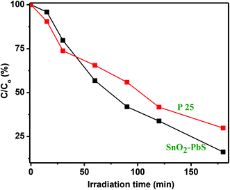
Catalyst recyclability and stability
To check the stability and reusability of the SnO2–PbS nanocomposite, cycling experiments on the photodegradation of RhB were undertaken with the catalyst recovered by centrifugation between tests. As illustrated in Fig. 11a, after three cycles of RhB photodegradation, the activity of SnO2–PbS nanocomposite revealed little loss of activity; the degradation efficiency of SnO2–PbS nanocomposite wrt RhB after the first, second, and third cycles being 84, 80, and 74%, respectively. The slightly reduced effectiveness of the catalyst in the third cycle can be tentatively attributed to photobleaching of the surface.64 Nevertheless, these data suggest SnO2–PbS nanocomposite to be stable and to avoid significant deactivation during RhB photodegradation. In addition to photocatalytic activity, the stability of photocatalysts is highly relevant to applications development and the crystalline structure of the SnO2–PbS nanocomposite has been investigated after photodegradation experiments. Fig. 11b illustrates the XRD patterns of photocatalysts before and after three RhB decomposition cycles, with the lack of observable changes indicating that both crystalline phase and structure remain intact.
 |
| | Fig. 11 (a) Reproducibility of the photocatalytic decomposition of RhB using fresh (cycle 1) and recycled (cycles 2 and 3) SnO2–PbS and (b) XRD patterns of SnO2–PbS nanocomposite before and after these tests. | |
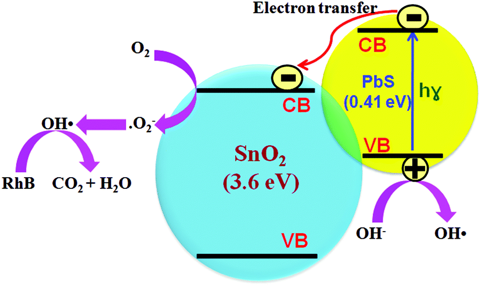
Product analysis and reaction mechanism
It is recognized that hydroxyl radicals produced by the illumination of photocatalysts represent the key active species in degrading organic molecules. Consistent with the thermodynamic obligation for creating OH˙, the valence band (VB) and the conduction band (CB) of the semiconductor photocatalyst should be positioned such that the oxidation potential of the hydroxyl radical (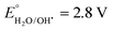 vs. normal hydrogen electrode (NHE)) and the reduction potential of superoxide radicals (
 vs. NHE) lie well within the band gap of the photocatalyst.65 The relative band positions of the two semiconductors were examined, as the band-edge potential plays a critical role in determining the transport of photoexcited charge carriers at a heterojunction. The low energy limits of the conduction band (ECB) of each component were estimated empirically according to66
| | | ECB/VB = X − 0.5Eg + E0 | (4) |
where Eg is the band gap energy of the semiconductor, E0 is the scale factor relating the reference electrode redox level to the absolute vacuum scale (E0 = −4.5 eV for NHE), and X is the electronegativity of the semiconductor, which can be expressed as the geometric mean of the absolute electronegativities of the constituent atoms. The X values for SnO2 and PbS are 2.59 and 2.19 eV, respectively, and the band gap energies of SnO2 and PbS are 3.61 and 0.41 eV, respectively. Following eqn (4) the ECB values of SnO2 and PbS become −3.72 and −2.52 eV, respectively. Likewise, the high energy limit of the valence bands (EVB) of SnO2 and PbS become −7.33 and −2.93 eV, respectively. This makes both the ECB and the EVB of PbS higher than their counterparts in SnO2. The bottom of the CB and the top of the VB of SnO2 lie at −0.78 and 2.83 eV with respect to NHE, whilst the corresponding values for PbS are −1.98 and −1.57 eV, meaning that neither SnO2 nor PbS can independently accomplish the thermodynamic prerequisite for OH˙ generation. Taking into account the band gap, ECB and EVB in PbS and SnO2 it follows that the band disposition of the SnO2–PbS nanocomposite promotes the separation and transportation of photoinduced charge carriers, leading to elevated photocatalytic activity. Fig. 12 shows how the type-II configuration of the nanocomposite diminishes the electron–hole recombination probability, allows one to boost electron mobility, and separates charge carriers; under irradiation, photogenerated electrons in PbS move to the SnO2, while the photogenerated holes are left in the valence band of PbS. Electron acceptors such as adsorbed O2 can trap electrons at the SnO2 surface to produce superoxide radical anions (O2−˙), which undergo protonation to yield hydroperoxy radicals ( ). In water, these then yield strongly oxidizing hydroxyl radicals (OH˙), which efficiently decompose organic pollutants like RhB. Lastly, photoinduced holes in PbS can also be trapped by OH−, so acting as another source of OH˙. Overall, the mechanism for the photocatalytic degradation of RhB can be expressed as:
| PbS + hv → PbS (eCB− + hVB+) |
| PbS (eCB−) + SnO2 → SnO2 (eCB−) + PbS |
| SnO2 (eCB−) + O2 → SnO2 + ˙O2− |
| PbS (hVB+) + OH− → OH˙ + PbS |
 |
| | Fig. 12 Model for the high photocatalytic activity and stability of SnO2–PbS nanocomposites. | |
To verify that photocatalytic degradation in the current system proceeds through photoinduced OH˙ radical formation a terephthalic acid (TA) probe was used, whereby reaction of TA with OH˙ radicals to generate fluorescent 2-hydroxyterephthalic acid (TAOH) was monitored.67 Upon excitation at 315 nm, the maximum intensity at 425 nm was determined to steadily increase with irradiation time (Fig. 13), indicating the photogeneration of OH˙. (Fig. S21† illustrates the linear increase in λmax = 425 nm with irradiation time.) Importantly, and in line with previous reports,67,68 the TA probe substantiates the photocatalytic mechanism proposed above, requiring the presence of a type-II system to explain radical formation.
 |
| | Fig. 13 Fluorescence spectral changes measured during illumination of SnO2–PbS nanocomposite in a basic solution of TA (excitation at 315 nm). | |
Measurement of apparent quantum yield
The apparent quantum yield (ϕx) of the SnO2–PbS nanocomposite with respect to aqueous RhB was determined using a 150 W xenon lamp fitted with an AM 1.5G filter (I = 100 mW cm−2). We calculated ϕx to be 0.217 mol min−1 W−1 using 5.0 mg catalyst in 40 mL of a 1.0 × 10⁻⁵ M aqueous solution of RhB at pH 7. In recycling tests (see above) ϕx values obtained for the 2nd and 3rd cycles were 0.214 and 0.208 mol min−1 W−1, respectively.
Comparison of photocatalytic activity with P25
The performance of the SnO2–PbS nanocomposite has been compared with that of the standard TiO2 Degussa P25 powder (P25).69 Results shown in Fig. S22† establish that P25 (5.0 mg) induces a steady decrease in the 555 nm absorption band of RhB with an efficiency which, at 70%, is low compared to that displayed by the new SnO2–PbS nanocomposite photocatalyst (84%) (Fig. 14).
 |
| | Fig. 14 A comparison of C/C0 (%) as a function of irradiation time for RhB solutions treated with SnO2–PbS nanocomposite and P25 (5.0 mg in either sample). | |
BET surface area analysis
The importance of surface area to heterogeneous photocatalysis derives from the ability of a larger surface area to furnish more active sites for the adsorption of reagent molecules.70 In this work, BET surface areas and pore size distributions were determined for SnO2 NPs and SnO2–PbS nanocomposites by measuring nitrogen adsorption–desorption isotherms (Fig. S23†). Both the adsorption and desorption branches of each of the recorded isotherms were found to be similar, meaning that they displayed type IV behaviour and distinct H2-type hysteresis loops.71 This suggests that either sample incorporates an interconnected network of mesopores63 with a disordered and inhomogeneous distribution of sizes72 characteristic of mesoporous structure formation through the aggregation of primary crystallites.73 Specific BET surface areas and pore volumes and sizes are summarized in Table 3. Notably, and in a similar vein to previous reports,74,75 the surface area of pure SnO2 NPs (128.0795 m2 g−1) exceeds that recorded for the SnO2–PbS nanocomposite (107.1704 m2 g−1), arguing against a simple correlation between surface area and photocatalytic activity.69 Taken together with the use of a TA probe to monitor photoinduced OH˙ radical formation, these results support a type-II interaction in the SnO2–PbS nanocomposite leading to the enhancement of photocatalytic activity.
Table 3 Nitrogen sorption porosimetry studiesa of as-synthesized SnO2 NPs and SnO2–PbS nanocomposites
| Photocatalyst |
S
BET (m2 g−1) |
Pore volume (cm3 g−1) |
Mean pore size (nm) |
|
Surface areas determined by the BET technique, mean pore diameters by BJH theory (applied to the adsorption branch), and pore volumes by single-point analysis.
|
| SnO2 |
128.0795 |
0.138662 |
3.8260 |
| SnO2–PbS |
107.1704 |
0.207755 |
6.6975 |
Conclusions
In summary, we have developed a facile and cost-effective approach to the synthesis of a SnO2–PbS nanocomposite, the nature of which has been comprehensively elucidated. Significantly, compared to pure SnO2, the SnO2–PbS nanocomposite displays enhanced photocatalytic activity and good structural stability for RhB degradation under simulated solar irradiation. An apparent quantum yield of 0.217 mol min−1 W−1 is calculated for the SnO2–PbS nanocomposite system and good recyclability is established. The composite structure is considered to improve the separation of photogenerated electron–hole pairs, thus enhancing the photocatalytic response. It is anticipated that this SnO2–PbS nanocomposite may provide a new approach to high performance, novel catalyst design and fabrication targeting new energy sources, green chemistry solutions, and addressing environmental issues. The facile synthetic method used is now being extended to other tin-containing nanocomposites, with efforts also being directed towards ensuring optimal recyclability, with an overall view to the design and cost-effective synthesis of advanced nanomaterials with specific properties for functional applications.
Acknowledgements
A. K. and D. R. acknowledge support from the Royal Society's Newton International Fellowship scheme. D. R. would also like to thank Prof. Paul Midgley for access to the TEM at the University of Cambridge and Prof. Gianluigi Botton for access to the CCEM, a national facility supported by NSERC, the Canada Foundation for Innovation and McMaster University. B. R. K. thanks the UK EPSRC for financial support (EP/J500380/1). Thanks go also to Drs Tim Jones and Jill Geddes of Schlumberger Gould Research for help with the acquisition of Raman and X-ray photoelectron spectra and to Dr Zlatko Saracevic of the Department of Chemical Engineering and Biotechnology (University of Cambridge) for help with BET surface area analysis. The authors would also like to thank Miss Georgina Hutton (University of Cambridge) for valuable discussions and input. Unprocessed data for this paper are available at the University of Cambridge data repository (see https://www.repository.cam.ac.uk/handle/1810/252973). These include some data in the file format .dm3 (HRTEM data), which can be opened using the software program Gatan Digital Micrograph 3.6.5 or similar.
References
- R. Roy, R. A. Roy and D. M. Roy, Mater. Lett., 1986, 4, 323–328 CrossRef.
- V. L. Colvin, M. C. Schlamp and A. P. Alivisatos, Nature, 1994, 370, 354–357 CrossRef CAS; B. O. Dabbousi, M. G. Bawendi, O. Onitsuka and M. F. Rubner, Appl. Phys. Lett., 1995, 66, 1316–1318 CrossRef.
- C. Lu, C. Guan, Y. Liu, Y. Cheng and B. Yang, Chem. Mater., 2005, 17, 2448–2454 CrossRef CAS; X. Lu, Y. Zhao and C. Wang, Adv. Mater., 2005, 17, 2485–2488 CrossRef.
- V. Salgueiriño-Maceira and M. A. Correa-Duarte, Adv. Mater., 2007, 19, 4131–4144 CrossRef CAS; B. Y. S. Kim, W. Jiang, J. Oreopoulos, C. M. Yip, J. T. Rutka and W. C. W. Chan, Nano Lett., 2008, 8, 3887–3892 CrossRef PubMed.
- K. Rajeshwar, N. R. de Tacconi and C. R. Chenthamarakshan, Chem. Mater., 2001, 13, 2765–2782 CrossRef CAS.
- P. H. C. Camargo, K. G. Satyanarayana and F. Wypych, Mater. Res., 2009, 12, 1–39 CrossRef CAS.
- J. Moczo and B. Pukanszky, J. Ind. Eng. Chem., 2008, 14, 535–563 CrossRef CAS.
- M. Rahmat and P. Hubert, Compos. Sci. Technol., 2011, 72, 72–84 CrossRef CAS.
- C. Ingrosso, A. Panniello, R. Comparelli, M. L. Curri and M. Striccoli, Materials, 2010, 3, 1316–1352 CrossRef CAS.
- Y. Wang, Acc. Chem. Res., 1991, 24, 133–139 CrossRef CAS.
- A. P. Alivisatos, Science, 1996, 271, 933–937 CAS.
- S. A. Haque, S. Koops, N. Tokmoldin, J. R. Durrant, J. S. Huang, D. D. C. Bradley and E. Palomares, Adv. Mater., 2007, 19, 683–687 CrossRef CAS.
- P. Ravirajan, D. D. C. Bradley, J. Nelson, S. A. Haque, J. R. Durrant, H. J. P. Smit and J. M. Kroon, Appl. Phys. Lett., 2005, 86, 143101 CrossRef.
- P. V. Kamat, J. Phys. Chem. C, 2008, 112, 18737–18753 CAS.
- S. M. Choi and H. Awaji, Sci. Technol. Adv. Mater., 2005, 6, 2–10 CrossRef CAS.
- A. Kar and A. Patra, J. Phys. Chem. C, 2009, 113, 4375–4380 CAS.
- P. G. Harrison and M. J. Willet, Nature, 1988, 332, 337–339 CrossRef.
- W. W. Wang, Y. J. Zhu and L. X. Yang, Adv. Funct. Mater., 2007, 17, 59–64 CrossRef CAS.
- J. Zhu, Z. Lu, S. T. Aruna, D. Aurbach and A. Gedanken, Chem. Mater., 2000, 12, 2557–2566 CrossRef CAS.
- Y. Wang, X. Jiang and Y. Xia, J. Am. Chem. Soc., 2003, 125, 16176–16177 CrossRef CAS PubMed.
- L. Zhang, H. Zhang, H. Huang, Y. Liu and Z. Kang, New J. Chem., 2012, 36, 1541–1544 RSC.
- J. T. McCue and J. Y. Ying, Chem. Mater., 2007, 19, 1009–1015 CrossRef CAS.
- J. Pan, J. Li, Z. Yan, B. Zhou, H. Wu and X. Xiong, Nanoscale, 2013, 5, 3022–3029 RSC.
- M. Taei, M. Shavakhi, H. Hadadzadeh, M. Movahedi, M. Rahimi and S. Habibollahi, J. Appl. Electrochem., 2015, 45, 185–195 CrossRef CAS.
- G. An, N. Na, X. Zhang, Z. Miao, S. Miao, K. Ding and Z. Liu, Nanotechnology, 2007, 18, 435707 CrossRef.
- R. K. Selvan, I. Perelshtein, N. Perkas and A. Gedanken, J. Phys. Chem. C, 2008, 112, 1825–1830 CAS.
- L. Wang, D. Wang, Z. Dong, F. Zhang and J. Jin, Nano Lett., 2013, 13, 1711–1716 CAS.
- A. Martucci, J. Fick, S.-E. Leblanc, M. Locascio and A. Hache, J. Non-Cryst. Solids, 2004, 345, 639–642 CrossRef.
- D. Berhanu, K. Govender, D. Smyth-Boyle, M. Archbold, D. P. Halliday and P. O'Brien, Chem. Commun., 2006, 4709–4711 RSC.
- S. B. Qadri, J. Yang, B. R. Ratna, E. F. Skelton and J. Z. Hu, Appl. Phys. Lett., 1996, 69, 2205–2207 CrossRef CAS.
- O. M. Ntwaeaborwa, R. E. Kroon, V. Kumar, T. Dubroca, J.-P. Ahn, J.-K. Park and H. C. Swart, J. Phys. Chem. Solids, 2009, 70, 1438–1442 CrossRef CAS.
- P. Ghosh, A. Kar and A. Patra, J. Appl. Phys., 2010, 108, 113506 CrossRef.
- W. Wu, L. Liao, S. Zhang, J. Zhou, X. Xiao, F. Ren, L. Sun, Z. Dai and C. Jiang, Nanoscale, 2013, 5, 5628–5636 RSC.
- A. Kar, A. Datta and A. Patra, J. Mater. Chem., 2010, 20, 916–922 RSC.
- T. Gao and T. Wang, Chem. Commun., 2004, 2558–2559 RSC.
- H. M. Rietveld, Acta Crystallogr., 1967, 22, 151–152 CrossRef CAS; H. M. Rietveld, J. Appl. Crystallogr., 1969, 2, 65–71 CrossRef; R. A. Young and D. B. Willes, J. Appl. Crystallogr., 1982, 15, 430–438 Search PubMed; L. Lutterotti, P. Scardi and P. Maistrelli, J. Appl. Crystallogr., 1992, 25, 459–462 CrossRef;
R. A. Young, The Rietveld Method, Oxford University Press Inc, New York, 1996 Search PubMed.
-
L. Lutterotti, Program Maud (version 2.33), http://maud.radiographema.com/ Search PubMed.
- HyperSpy homepage hyperspy.org.
- Y. Xu and C. H. Langford, Langmuir, 2001, 17, 897–902 CrossRef CAS.
- J. M. Buriak, P. V. Kamat and K. S. Schanze, ACS Appl. Mater. Interfaces, 2014, 6, 11815–11816 CAS.
- S. Sain, A. Kar, A. Patra and S. K. Pradhan, CrystEngComm, 2014, 16, 1079–1090 RSC.
-
B. E. Warren, X-ray Diffraction, Addison-Wesley, Reading, MA, 1969 Search PubMed.
- H. Dutta, S. K. Manik and S. K. Pradhan, J. Appl. Crystallogr., 2003, 36, 260–268 CrossRef CAS.
- D. Rossouw, P. Burdet, F. de la Peña, C. Ducati, B. R. Knappett, A. E. H. Wheatley and P. A. Midgley, Nano Lett., 2015, 15, 2716–2720 CrossRef CAS PubMed.
- A. Kar, S. Kundu and A. Patra, J. Phys. Chem. C, 2011, 115, 118–124 CAS.
- G. Xi and J. Ye, Inorg. Chem., 2010, 49, 2302–2309 CrossRef CAS PubMed.
- F. Gu, S. F. Wang, M. K. Lu, G. J. Zhou, D. Xu and D. R. Yuan, J. Phys. Chem. B, 2004, 108, 8119–8123 CrossRef CAS.
- H. Cao, G. Wang, S. Zhang and X. Zhang, Nanotechnology, 2006, 17, 3280–3287 CrossRef CAS.
- Y.-D. Wang, C.-L. Ma, X.-D. Sun and H.-D. Li, Nanotechnology, 2002, 13, 565–569 CrossRef CAS.
- D. Chen and L. Gao, J. Colloid Interface Sci., 2004, 279, 137–142 CrossRef CAS PubMed; Q. Li, X. D. Yuan, G. F. Zeng and S. Q. Xi, Mater. Chem. Phys., 1997, 47, 239–245 CrossRef; W. Y. Chung, D. D. Lee and B. K. Sohn, Thin Solid Films, 1992, 221, 304–310 CrossRef.
- R. S. C. Smart, W. M. Skinner and A. R. Gerson, Surf. Interface Anal., 1999, 28, 101–105 CrossRef CAS; M. Takahashi, Y. Ohshima, K. Nagata and S. Furuta, J. Electroanal. Chem., 1993, 359, 281–286 CrossRef.
- A. Lobo, T. Moller, M. Nagel, H. Borchert, S. G. Hickey and H. Weller, J. Phys. Chem. B, 2005, 109, 17422–17428 CrossRef CAS PubMed.
-
J. F. Moulder, W. F. Stickle, P. E. Sobol and K. D. Bomben, in Handbook of X-ray Photoelectroscopy, Physical Electronics, ed. J. Chastain, MN, 1995 Search PubMed.
- R. S. C. Smart, W. M. Skinner and A. R. Gerson, Surf. Interface Anal., 1999, 28, 101–105 CrossRef CAS; M. Takahashi, Y. Ohshima, K. Nagata and S. Furuta, J. Electroanal. Chem., 1993, 359, 281–286 CrossRef.
- S. Chen and W. Liu, Mater. Chem. Phys., 2006, 98, 183–189 CrossRef CAS.
- L. Cao, H. Wan, L. Huo and S. Hi, J. Colloid Interface Sci., 2001, 244, 97–101 CrossRef CAS.
- S. Chen and W. Liu, Mater. Chem. Phys., 2006, 98, 183–189 CrossRef CAS.
- Y. Q. Wang, S. G. Chen, X. H. Tang, O. Palchik, A. Zaban, Y. Koltypin and A. Gedanken, J. Mater. Chem., 2001, 11, 521–526 RSC.
- S.-Y. Chen, H.-D. Tsai, W.-T. Chuang, J.-J. Lee, C.-Y. Tang, C.-Y. Lin and S. Cheng, J. Phys. Chem. C, 2009, 113, 15226–15238 CAS.
- A. H. Souici, N. Keghouche, J. A. Delaire, H. Remita, A. Etcheberry and M. Mostafavi, J. Phys. Chem. C, 2009, 113, 8050–8057 Search PubMed; M. Yousefi, F. Gholamian, D. Ghanbari and M. Salavati-Niasari, Polyhedron, 2011, 30, 1055–1060 CrossRef CAS; S. Jing, S. Xing and C. Zhao, Mater. Lett., 2008, 62, 41–43 CrossRef.
- W. W. Wang, Y. J. Zhu and L. X. Yang, Adv. Funct. Mater., 2007, 17, 59–64 CrossRef CAS.
- O. M. Ntwaeaborwa, R. E. Kroon, V. Kumar, T. Dubroca, J.-P. Ahn, J.-K. Park and H. C. Swart, J. Phys. Chem. Solids, 2009, 70, 1438–1442 CrossRef.
- Y. Feng, L. Li, M. Ge, C. Guo, J. Wang and L. Liu, ACS Appl. Mater. Interfaces, 2010, 2, 3134–3140 Search PubMed.
- Y. Yang, D. S. Kim, Y. Qin, A. Berger, R. Scholz, H. Kim, M. Knez and U. Gösele, J. Am. Chem. Soc., 2009, 131, 13920–13921 CrossRef PubMed.
- R. Vinu and G. J. Madras, J. Indian Inst. Sci., 2010, 90, 189–230 Search PubMed.
- Z. Zhang, W. Wang, L. Wang and S. Sun, ACS Appl. Mater. Interfaces, 2012, 4, 593–597 Search PubMed.
- S. Khanchandani, S. Kundu, A. Patra and A. K. Ganguli, J. Phys. Chem. C, 2013, 117, 5558–5567 Search PubMed.
- R. Bera, S. Kundu and A. Patra, ACS Appl. Mater. Interfaces, 2015, 7, 13251–13259 Search PubMed; C. Wang, C. Shao, X. Zhang and Y. Liu, Inorg. Chem., 2009, 48, 7261–7268 CrossRef PubMed.
- A. Kar, S. Sain, S. Kundu, A. Bhattacharyya, S. K. Pradhan and A. Patra, ChemPhysChem, 2015, 16, 1017–1025 CrossRef PubMed.
- J. Yu, S. Liu and H. Yu, J. Catal., 2007, 249, 59–66 CrossRef; J. Yu, G. Wang, B. Cheng and M. Zhou, Appl. Catal., B, 2007, 69, 171–180 CrossRef.
- K. S. W. Sing, D. H. Everett, R. A. W. Haul, L. Moscou, R. A. Pierotti, J. Rouquerol and T. Siemieniewska, Pure Appl. Chem., 1985, 57, 603–619 CrossRef CAS; E. L. Foletto, S. Battiston, G. C. Collazzo, M. M. Bassaco and M. A. Mazutti, Water, Air, Soil Pollut., 2012, 223, 5773–5779 CrossRef.
- H.-C. Chiu and C.-S. Yeh, J. Phys. Chem. C, 2007, 111, 7256–7259 CAS.
- K. J. A. Raj and B. Viswanathan, ACS Appl. Mater. Interfaces, 2009, 1, 2462–2469 CAS.
- Y. C. Zhang, Z. N. Du, K. W. Li, M. Zhang and D. D. Dionysiou, ACS Appl. Mater. Interfaces, 2011, 3, 1528–1537 CAS.
- M. T. Uddin, Y. Nicolas, C. Olivier, T. Toupance, L. Servant, M. M. Müller, H.-J. Kleebe, J. Ziegler and W. Jaegermann, Inorg. Chem., 2012, 51, 7764–7773 CrossRef CAS PubMed.
Footnote |
| † Electronic supplementary information (ESI) available. See DOI: 10.1039/c5nr07036h |
|
| This journal is © The Royal Society of Chemistry 2016 |
Click here to see how this site uses Cookies. View our privacy policy here. 
 Open Access Article
 This Open Access Article is licensed under a


 vs. normal hydrogen electrode (NHE)) and the reduction potential of superoxide radicals (
 vs. NHE) lie well within the band gap of the photocatalyst.65 The relative band positions of the two semiconductors were examined, as the band-edge potential plays a critical role in determining the transport of photoexcited charge carriers at a heterojunction. The low energy limits of the conduction band (ECB) of each component were estimated empirically according to66
 ). In water, these then yield strongly oxidizing hydroxyl radicals (OH˙), which efficiently decompose organic pollutants like RhB. Lastly, photoinduced holes in PbS can also be trapped by OH−, so acting as another source of OH˙. Overall, the mechanism for the photocatalytic degradation of RhB can be expressed as: